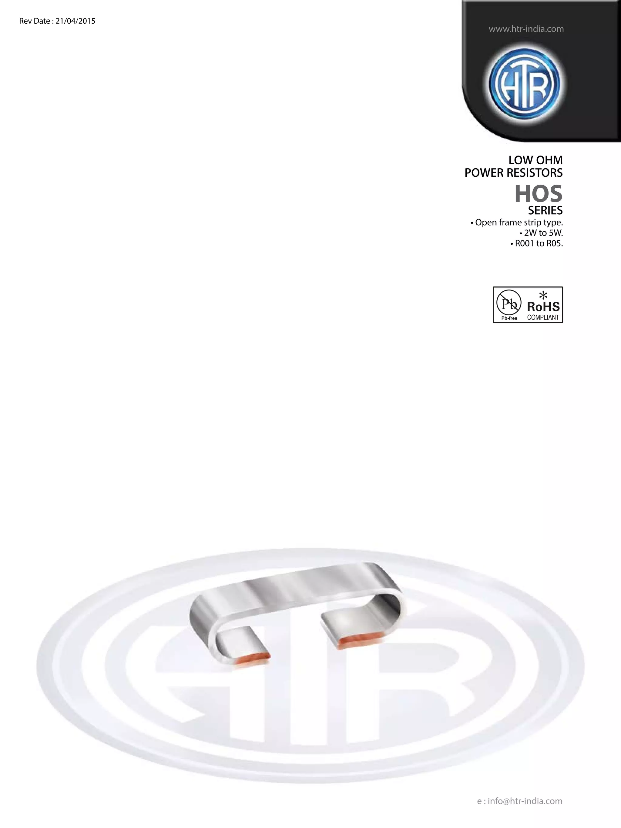
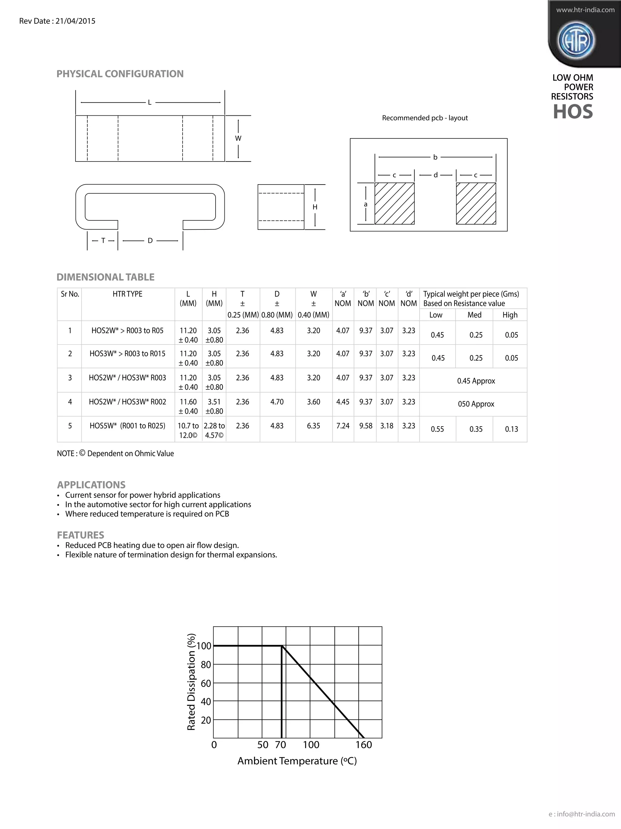
• Open frame strip type.
• 2W to 5W.
• R001 to R05.
LOW OHM
POWER RESISTORS
HOS
SERIES
Size 4512
e : info@htr-india.com
www.htr-india.com
Rev Date : 28/06/2017
Asper AEC-Q200
PHYSICAL CONFIGURATION
DIMENSIONAL TABLE
LOW OHM
POWER
RESISTORS
HOS
Size 4512
e : info@htr-india.com
www.htr-india.com
	 Sr No.	 HTR TYPE	 L	 H	 T	 D	 W	 ‘a’	 ‘b’	 ‘c’	 ‘d’	
			 (mm)	 (mm)	 ±	 ±	 ±	 nom 	nom 	nom 	nom
					 0.25 (mm)	0.80 (mm)	 0.40 (mm)					 Low	Med	 High	
	 1	 HOS2W* > R003 to R05	 11.20	 3.05	 2.36	 4.83	 3.20	 4.07	 9.37	 3.07	 3.23
			 ± 0.40	 ±0.80
	 2	 HOS3W* > R003 to R05	 11.20	 3.05	 2.36	 4.83	 3.20	 4.07	 9.37	 3.07	 3.23
			 ± 0.40	 ±0.80
	 3	 HOS2W* / HOS3W* R003	 11.20	 3.51	 2.36	 4.83	 3.20	 4.07	 9.37	 3.07	 3.23
			 ± 0.40	 ±0.80
	 4	 HOS2W* / HOS3W* R002	 11.60	 3.51	 2.36	 4.70	 3.60	 4.45	 9.37	 3.07	 3.23
			 ± 0.40	 ±0.80
	 5	 HOS5W* R001 to R025	 10.7 to	 2.28 to	 2.36	 4.83	 6.35	 7.24	 9.58	 3.18	 3.23
			 12.0©	 4.57©
Typical weight per piece (Gms)
Based on Resistance value
	 0.45	 0.25	 0.05
	 0.45	 0.25	 0.05
		 0.45 Approx
		 050 Approx
	 0.55	 0.35	 0.13
NOTE : © Dependent on Ohmic Value
APPLICATIONS
• 	 Current sensor for power hybrid applications
•	 In the automotive sector for high current applications
•	 Where reduced temperature is required on PCB
FEATURES
• 	 Reduced PCB heating due to open air flow design as compared to flat chip format.
•	 Flexible nature of termination design for thermal expansions.
Rev Date : 28/06/2017
L
W
T D
H a
b
c cd
Recommended PCB - layout
Recommended PCB layout for normal application
Recommended PCB layout for high precision applications : Kelvin (4 terminal pad design) is sug-
gestedasperillustrationbelow.Thehighcurrentconnectionsaremadetothetwopairsoflarger
pads and the voltage sense connections are made to the two smaller central pads.
10.57
7.11
3.23
1.52
2.79
3.67 3.67
Note:
Recommended
voltege sense pads
for Kelvin connection
2.79
3.16
0.51
0.51
0.51
L
W
T D
H a
b
c cd
Recommended PCB - layout
HOS5W* 4 terminal pad design
Dimensions in mm
LOW OHM
POWER
RESISTORS
HOS
Size 4512
e : info@htr-india.com
www.htr-india.com
Rev Date : 28/06/2017
Note :
Temperature rise data
are given here for typical
mounting conditions. Ac-
tual figures depend on PCB
copper weight, mounting
pad size, track width and
substrate type. Also, the
open air format responds
better to forced air cooling
than chip format resistors.
For values below 5 mil-
liohms allowance should
be made for heat generated
in the copper tracks them-
selves. Application-specific
guidance is available on re-
quest from our application
laboratory.
Hot Spot Temperature Rise
Mounting data : 7.6mm X 7.6mm pads, 2 oz copper on FR4, still air
25%
0
50
100
150
200
250
300
50% 75% 100%
TemperatureRise(K)
Percentage of Rated Power
Resistance Value
in milliohms
HOS 2W / 3W & 5W
50 / 25
30 /15
10 / 5
5 / -
Solder Joint Temperature Rise
Mounting data : 7.6mm X 7.6mm pads, 2 oz copper on FR4, still air
25%
0
20
40
60
80
100
50% 75% 100%
TemperatureRise(K)
Percentage of Rated Power
Resistance Value
in milliohms
HOS 2W / 3W & 5W
5 / -
10 / 5
30 / 15
50 / 25
0
20
40
60
80
100
50 100 150 200 250
RatedDissipation(%)
Ambient Temperature (ºC)
Temperature Derating
Resistance Value in milliohms
Pulse Energy Rating
NOTE : This graph relates to single pulses of short duration (≤ 100ms).
Higher energy limits apply for longer pulses and overloads.
HOS 2W / HOS 3W HOS 5W
0
1
20
40
60
80
100
120
10 100
Energy(J)
e : info@htr-india.com
www.htr-india.com
ELECTRICAL AND ENVIRONMENTAL CHARACTERISTICS
Power Rating (Rated Ambient Temperature )	 Full power dissipation at 70° C and linearly
	 de-rated to zero at + 225° C
Insulation	 Not Insulated
Resistance Tolerance 	 ± 5% (Available up to ± 1%)
Inductance	 < 10 nH
Operating Temperature Range	 - 55° C to +160° C
Voltage Rating / Limiting Voltage / Max. Working Voltage	 P x R
subject to max. terminal temperature + 120° C	
	 For – HOS2W & HOS3W
	 240ppm – For Resistance value < R004.
	 40ppm – For Resistance value R004 to R015
	 40ppm – For Resistance value > R015.
Temperature Co-efficient of Resistance	 For – HOS5W
[Measured from 0°C to +125°C]	 240ppm – For Resistance value < R002.
	 40ppm – For Resistance value R002 to R007.
	 40ppm – For Resistance value > R007.
Thermal Shock 	 ∆R ± [ 0.75 ] – Average
	 For – HOS2W  HOS3W
	 ∆R ± [  1.0 % ] – For Resistance value  R004.
	 ∆R ± [  1.0 % ] – For Resistance value R004 to R015.
Temperature Cycling	 ∆R ± [  0.75 % ] – For Resistance value  R015.
[Room temperature -55°C Room temperature 125°C	 For – HOS5W
Room temperature for 5 cycles]	 ∆R ± [  1.0 % ] – For Resistance value  R002.
	 ∆R ± [  1.0 % ] – For Resistance value R002 to R007.
	 ∆R ± [  0.75 % ] – For Resistance value  R007.
	 For – HOS2W  HOS3W
	 ∆R ± [  1.75 % ] – For Resistance value  R004.
	 ∆R ± [  0.5 % ] – For Resistance value R004 to R015.
	 ∆R ± [  1.0 % ] – For Resistance value  R015.
High Temp. Exposure ( 125°C- For 2 Hrs.)	 For – HOS5W
	 ∆R ± [  1.75 % ] – For Resistance value  R002.
	 ∆R ± [  0.5 % ] – For Resistance value R002 to R007.
	 ∆R ± [  1.0 % ] – For Resistance value  R007.
Damp Heat ( Steady State )	 ∆R ± [ 0.5 % ] – Average
( 40°C at 93 % R.H. for 1000 Hrs. – no load applied )	
	 For – HOS2W  HOS3W
	 ∆R ± [  2.0 % ] – For Resistance value  R004.
	 ∆R ± [  1.0 % ] – For Resistance value R004 to R015.
Endurance – Load Life	 ∆R ± [  1.0 % ] – For Resistance value  R015.
[ 70°C with limiting voltage – 	 For – HOS5W
with temperature limitation on terminal kept at 120°C	 ∆R ± [  2.0 % ] – For Resistance value  R002.
1.5 hours on / 0.5 hours off for 1000 hours]	 ∆R ± [  1.0 % ] – For Resistance value R002 to R007.
	 ∆R ± [  1.0 % ] – For Resistance value  R007.
Bias Humidity [+85° C, 85% RH, 1000h]	 ∆R ± 0.5% -Typical
Mechanical Shock [100 g. 6 ms half sine]	 ∆R ± 0.5% -Typical
Vibration, High Frequency [20 g. 10-2000 Hz]	 ∆R ± 0.5% -Typical
LowTemperature Storage and Operation [-65° C for 24 h]	 ∆R ± 0.2% -Typical
Moisture Resistance [MIL-STD-202 method106]	 ∆R ± 0.2% -Typical
PARAMETER / PERFORMANCE TEST  TEST METHOD 	 PERFORMANCE REQUIREMENTS
HOT SPOT TEMPERATURE RISE (IN STILL AIR) - 	
From 180 °C to 280 °C at 100% power depending on the resistance value, pad and PCB thickness. Due to the nature of it’s construc-
tion, the HOS resistor keeps the hot spot from a thermal point of view from the solder joints and reduces the possibility of transfer
of high temperature on to the PCB in contrast to the flat chip format.
SOLDER JOINT TEMPERATURE RISE (IN STILL AIR) - 	
From 60 °C to 85 °C at 100% power depending upon resistance value, pad and PCB thickness.
CONSTRUCTION :
The copper terminals are electron beam welded to the requisite alloy strip and then formed. Value variations are possible by varia-
tions of width without traditional abrasion / notch trimming.
Rev Date : 28/06/2017
LOW OHM
POWER
RESISTORS
HOS
Size 4512
www.htr-india.com
e : info@htr-india.com
PACKAGING
A. BULK
1000 resistors are packed in sealed plastic packets with silica gel pouch and place in small cardboard carton (Type ‘I’ box) approx size
70 x 70 x 70 mm and 4 such boxes can be packed in Type ‘A’ box approx size 200 x 150 x 70mm. 36 boxes (36000 pieces) of Type ‘’I’ or 6
boxes (24000 pieces) of Type‘A’can be packed in master carton of approx size 320 x 245 x 245mm.
B. TAPE  REEL PACKING
Storage Condition (Packed) : Temp 25°C to 35°C, Humidity 30 to 80% RH, Shelf life-12 months
Floor Life (Unpacked) : Temp 25°C to 35°C, Humidity 30 to 80% RH, Floor life-15 days
+_
	
DIMENSIONAL TABLE
	Sr No.	 HTR TYPE	 A(mm)	 B(mm)	 C(mm)	 D(mm)	 E(mm)	 F(mm)	 G(mm)	 H(mm)	 PCS/Reel
	 1	 HOS2W  HOS3W ≥ R003	 4.32±0.1	 11.7±0.1	 24±0.3	 11.5±0.1 	 1.75±0.1	 8.0±0.1	 4.0±0.1	 4.5±0.1	 1800 pcs.
	 2	 HOS2W  HOS3W R002	 4.32±0.1	 12.1±0.1	 24±0.3	 11.5±0.1 	 1.75±0.1	 8.0±0.1	 4.0±0.1	 4.5±0.1	 1800 pcs.
	 3	 HOS5W	 7.21±0.1	 12.1±0.1	 24±0.3	 11.5±0.1 	 1.75±0.1	 12.0±0.1	 4.0±0.1	 4.5±0.1	 1100 pcs.
Rev Date : 28/06/2017
RECOMMENDED SOLDER PROFILE
Reflow, IR - and wave soldering
Temperature (°C)	 260	 255	 217
Time (Sec)		 Peak	 40	 90
LOW OHM
POWER
RESISTORS
HOS
Size 4512
MECHANICAL SPECIFICATIONS
Resistance to Soldering heat - (350° C for 30 Secs)	 ∆ R ± [ 0.2 % ] – Typical
Solderabillity (Meets J-STD-002 Method B)	Must meet the requirements laid down
Solvent Resistance (Meets MIL-STD-002 Method 215)	Must meet the requirements laid down
PARAMETER / PERFORMANCE TEST  TEST METHOD 	 PERFORMANCE REQUIREMENTS

HOS - LOW OHM POWER RESISTORS

  • 1.
    • Open framestrip type. • 2W to 5W. • R001 to R05. LOW OHM POWER RESISTORS HOS SERIES Size 4512 e : info@htr-india.com www.htr-india.com Rev Date : 28/06/2017 Asper AEC-Q200
  • 2.
    PHYSICAL CONFIGURATION DIMENSIONAL TABLE LOWOHM POWER RESISTORS HOS Size 4512 e : info@htr-india.com www.htr-india.com Sr No. HTR TYPE L H T D W ‘a’ ‘b’ ‘c’ ‘d’ (mm) (mm) ± ± ± nom nom nom nom 0.25 (mm) 0.80 (mm) 0.40 (mm) Low Med High 1 HOS2W* > R003 to R05 11.20 3.05 2.36 4.83 3.20 4.07 9.37 3.07 3.23 ± 0.40 ±0.80 2 HOS3W* > R003 to R05 11.20 3.05 2.36 4.83 3.20 4.07 9.37 3.07 3.23 ± 0.40 ±0.80 3 HOS2W* / HOS3W* R003 11.20 3.51 2.36 4.83 3.20 4.07 9.37 3.07 3.23 ± 0.40 ±0.80 4 HOS2W* / HOS3W* R002 11.60 3.51 2.36 4.70 3.60 4.45 9.37 3.07 3.23 ± 0.40 ±0.80 5 HOS5W* R001 to R025 10.7 to 2.28 to 2.36 4.83 6.35 7.24 9.58 3.18 3.23 12.0© 4.57© Typical weight per piece (Gms) Based on Resistance value 0.45 0.25 0.05 0.45 0.25 0.05 0.45 Approx 050 Approx 0.55 0.35 0.13 NOTE : © Dependent on Ohmic Value APPLICATIONS • Current sensor for power hybrid applications • In the automotive sector for high current applications • Where reduced temperature is required on PCB FEATURES • Reduced PCB heating due to open air flow design as compared to flat chip format. • Flexible nature of termination design for thermal expansions. Rev Date : 28/06/2017 L W T D H a b c cd Recommended PCB - layout Recommended PCB layout for normal application Recommended PCB layout for high precision applications : Kelvin (4 terminal pad design) is sug- gestedasperillustrationbelow.Thehighcurrentconnectionsaremadetothetwopairsoflarger pads and the voltage sense connections are made to the two smaller central pads. 10.57 7.11 3.23 1.52 2.79 3.67 3.67 Note: Recommended voltege sense pads for Kelvin connection 2.79 3.16 0.51 0.51 0.51 L W T D H a b c cd Recommended PCB - layout HOS5W* 4 terminal pad design Dimensions in mm
  • 3.
    LOW OHM POWER RESISTORS HOS Size 4512 e: info@htr-india.com www.htr-india.com Rev Date : 28/06/2017 Note : Temperature rise data are given here for typical mounting conditions. Ac- tual figures depend on PCB copper weight, mounting pad size, track width and substrate type. Also, the open air format responds better to forced air cooling than chip format resistors. For values below 5 mil- liohms allowance should be made for heat generated in the copper tracks them- selves. Application-specific guidance is available on re- quest from our application laboratory. Hot Spot Temperature Rise Mounting data : 7.6mm X 7.6mm pads, 2 oz copper on FR4, still air 25% 0 50 100 150 200 250 300 50% 75% 100% TemperatureRise(K) Percentage of Rated Power Resistance Value in milliohms HOS 2W / 3W & 5W 50 / 25 30 /15 10 / 5 5 / - Solder Joint Temperature Rise Mounting data : 7.6mm X 7.6mm pads, 2 oz copper on FR4, still air 25% 0 20 40 60 80 100 50% 75% 100% TemperatureRise(K) Percentage of Rated Power Resistance Value in milliohms HOS 2W / 3W & 5W 5 / - 10 / 5 30 / 15 50 / 25 0 20 40 60 80 100 50 100 150 200 250 RatedDissipation(%) Ambient Temperature (ºC) Temperature Derating Resistance Value in milliohms Pulse Energy Rating NOTE : This graph relates to single pulses of short duration (≤ 100ms). Higher energy limits apply for longer pulses and overloads. HOS 2W / HOS 3W HOS 5W 0 1 20 40 60 80 100 120 10 100 Energy(J)
  • 4.
    e : info@htr-india.com www.htr-india.com ELECTRICALAND ENVIRONMENTAL CHARACTERISTICS Power Rating (Rated Ambient Temperature ) Full power dissipation at 70° C and linearly de-rated to zero at + 225° C Insulation Not Insulated Resistance Tolerance ± 5% (Available up to ± 1%) Inductance < 10 nH Operating Temperature Range - 55° C to +160° C Voltage Rating / Limiting Voltage / Max. Working Voltage P x R subject to max. terminal temperature + 120° C For – HOS2W & HOS3W 240ppm – For Resistance value < R004. 40ppm – For Resistance value R004 to R015 40ppm – For Resistance value > R015. Temperature Co-efficient of Resistance For – HOS5W [Measured from 0°C to +125°C] 240ppm – For Resistance value < R002. 40ppm – For Resistance value R002 to R007. 40ppm – For Resistance value > R007. Thermal Shock ∆R ± [ 0.75 ] – Average For – HOS2W HOS3W ∆R ± [ 1.0 % ] – For Resistance value R004. ∆R ± [ 1.0 % ] – For Resistance value R004 to R015. Temperature Cycling ∆R ± [ 0.75 % ] – For Resistance value R015. [Room temperature -55°C Room temperature 125°C For – HOS5W Room temperature for 5 cycles] ∆R ± [ 1.0 % ] – For Resistance value R002. ∆R ± [ 1.0 % ] – For Resistance value R002 to R007. ∆R ± [ 0.75 % ] – For Resistance value R007. For – HOS2W HOS3W ∆R ± [ 1.75 % ] – For Resistance value R004. ∆R ± [ 0.5 % ] – For Resistance value R004 to R015. ∆R ± [ 1.0 % ] – For Resistance value R015. High Temp. Exposure ( 125°C- For 2 Hrs.) For – HOS5W ∆R ± [ 1.75 % ] – For Resistance value R002. ∆R ± [ 0.5 % ] – For Resistance value R002 to R007. ∆R ± [ 1.0 % ] – For Resistance value R007. Damp Heat ( Steady State ) ∆R ± [ 0.5 % ] – Average ( 40°C at 93 % R.H. for 1000 Hrs. – no load applied ) For – HOS2W HOS3W ∆R ± [ 2.0 % ] – For Resistance value R004. ∆R ± [ 1.0 % ] – For Resistance value R004 to R015. Endurance – Load Life ∆R ± [ 1.0 % ] – For Resistance value R015. [ 70°C with limiting voltage – For – HOS5W with temperature limitation on terminal kept at 120°C ∆R ± [ 2.0 % ] – For Resistance value R002. 1.5 hours on / 0.5 hours off for 1000 hours] ∆R ± [ 1.0 % ] – For Resistance value R002 to R007. ∆R ± [ 1.0 % ] – For Resistance value R007. Bias Humidity [+85° C, 85% RH, 1000h] ∆R ± 0.5% -Typical Mechanical Shock [100 g. 6 ms half sine] ∆R ± 0.5% -Typical Vibration, High Frequency [20 g. 10-2000 Hz] ∆R ± 0.5% -Typical LowTemperature Storage and Operation [-65° C for 24 h] ∆R ± 0.2% -Typical Moisture Resistance [MIL-STD-202 method106] ∆R ± 0.2% -Typical PARAMETER / PERFORMANCE TEST TEST METHOD PERFORMANCE REQUIREMENTS HOT SPOT TEMPERATURE RISE (IN STILL AIR) - From 180 °C to 280 °C at 100% power depending on the resistance value, pad and PCB thickness. Due to the nature of it’s construc- tion, the HOS resistor keeps the hot spot from a thermal point of view from the solder joints and reduces the possibility of transfer of high temperature on to the PCB in contrast to the flat chip format. SOLDER JOINT TEMPERATURE RISE (IN STILL AIR) - From 60 °C to 85 °C at 100% power depending upon resistance value, pad and PCB thickness. CONSTRUCTION : The copper terminals are electron beam welded to the requisite alloy strip and then formed. Value variations are possible by varia- tions of width without traditional abrasion / notch trimming. Rev Date : 28/06/2017 LOW OHM POWER RESISTORS HOS Size 4512
  • 5.
    www.htr-india.com e : info@htr-india.com PACKAGING A.BULK 1000 resistors are packed in sealed plastic packets with silica gel pouch and place in small cardboard carton (Type ‘I’ box) approx size 70 x 70 x 70 mm and 4 such boxes can be packed in Type ‘A’ box approx size 200 x 150 x 70mm. 36 boxes (36000 pieces) of Type ‘’I’ or 6 boxes (24000 pieces) of Type‘A’can be packed in master carton of approx size 320 x 245 x 245mm. B. TAPE REEL PACKING Storage Condition (Packed) : Temp 25°C to 35°C, Humidity 30 to 80% RH, Shelf life-12 months Floor Life (Unpacked) : Temp 25°C to 35°C, Humidity 30 to 80% RH, Floor life-15 days +_ DIMENSIONAL TABLE Sr No. HTR TYPE A(mm) B(mm) C(mm) D(mm) E(mm) F(mm) G(mm) H(mm) PCS/Reel 1 HOS2W HOS3W ≥ R003 4.32±0.1 11.7±0.1 24±0.3 11.5±0.1 1.75±0.1 8.0±0.1 4.0±0.1 4.5±0.1 1800 pcs. 2 HOS2W HOS3W R002 4.32±0.1 12.1±0.1 24±0.3 11.5±0.1 1.75±0.1 8.0±0.1 4.0±0.1 4.5±0.1 1800 pcs. 3 HOS5W 7.21±0.1 12.1±0.1 24±0.3 11.5±0.1 1.75±0.1 12.0±0.1 4.0±0.1 4.5±0.1 1100 pcs. Rev Date : 28/06/2017 RECOMMENDED SOLDER PROFILE Reflow, IR - and wave soldering Temperature (°C) 260 255 217 Time (Sec) Peak 40 90 LOW OHM POWER RESISTORS HOS Size 4512 MECHANICAL SPECIFICATIONS Resistance to Soldering heat - (350° C for 30 Secs) ∆ R ± [ 0.2 % ] – Typical Solderabillity (Meets J-STD-002 Method B) Must meet the requirements laid down Solvent Resistance (Meets MIL-STD-002 Method 215) Must meet the requirements laid down PARAMETER / PERFORMANCE TEST TEST METHOD PERFORMANCE REQUIREMENTS