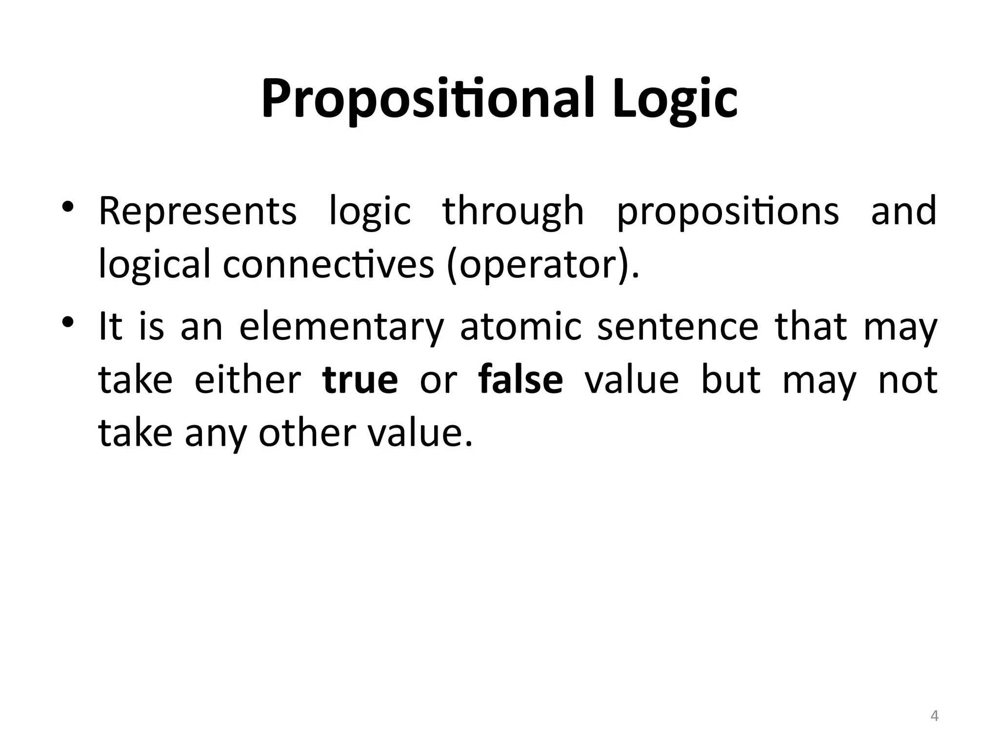
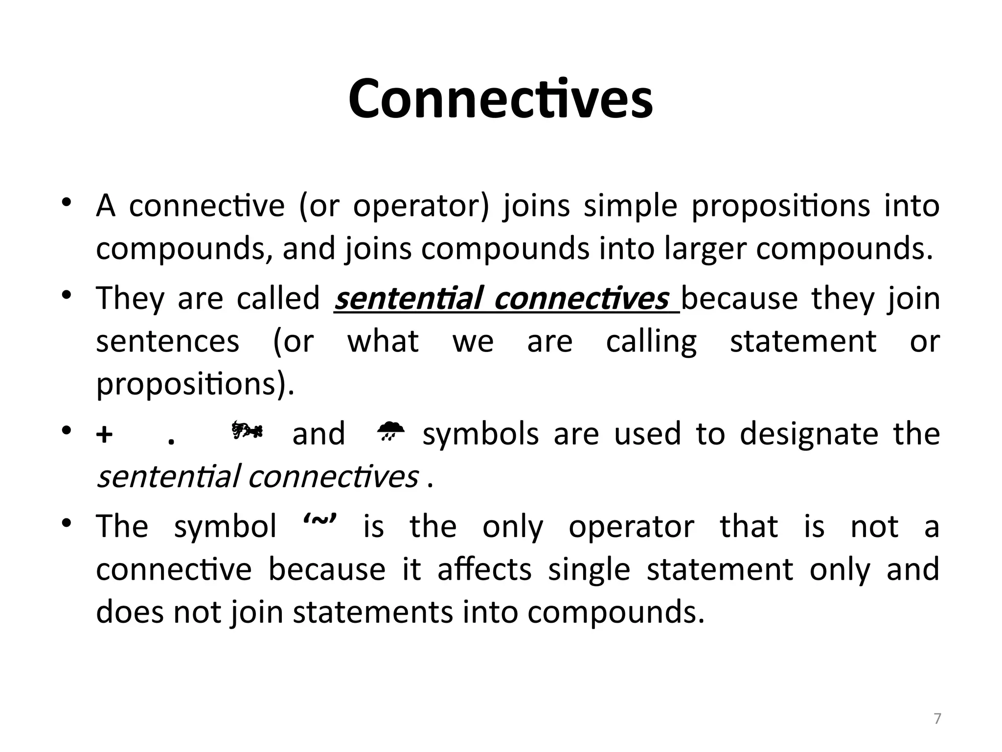
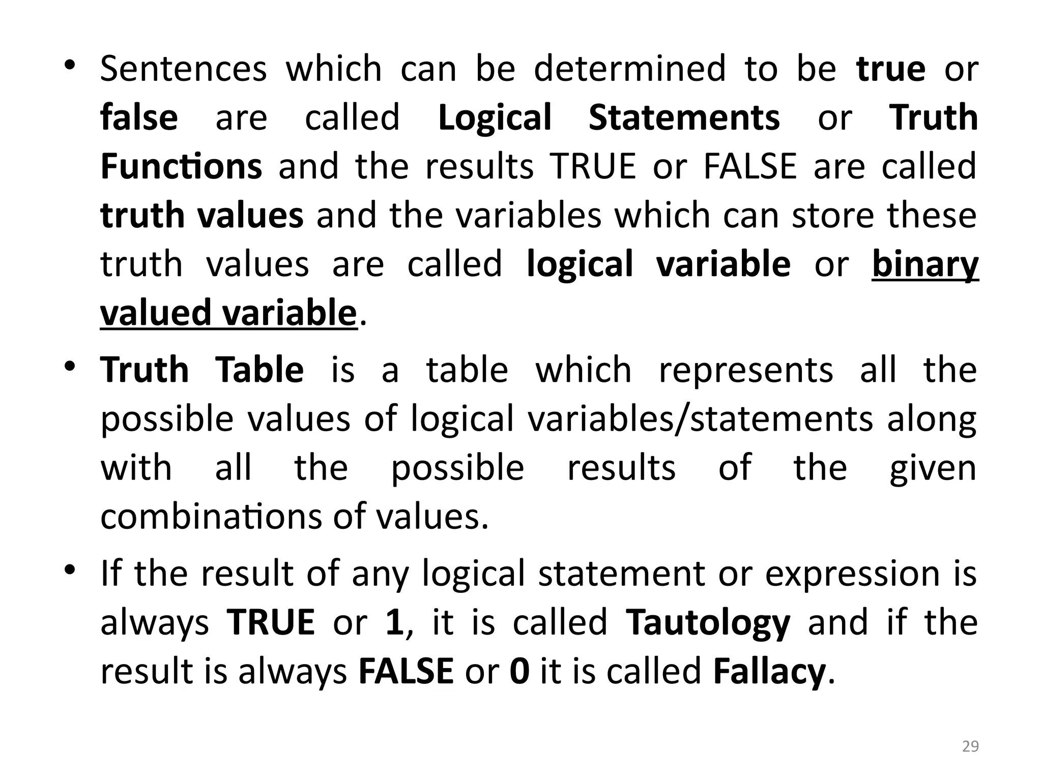
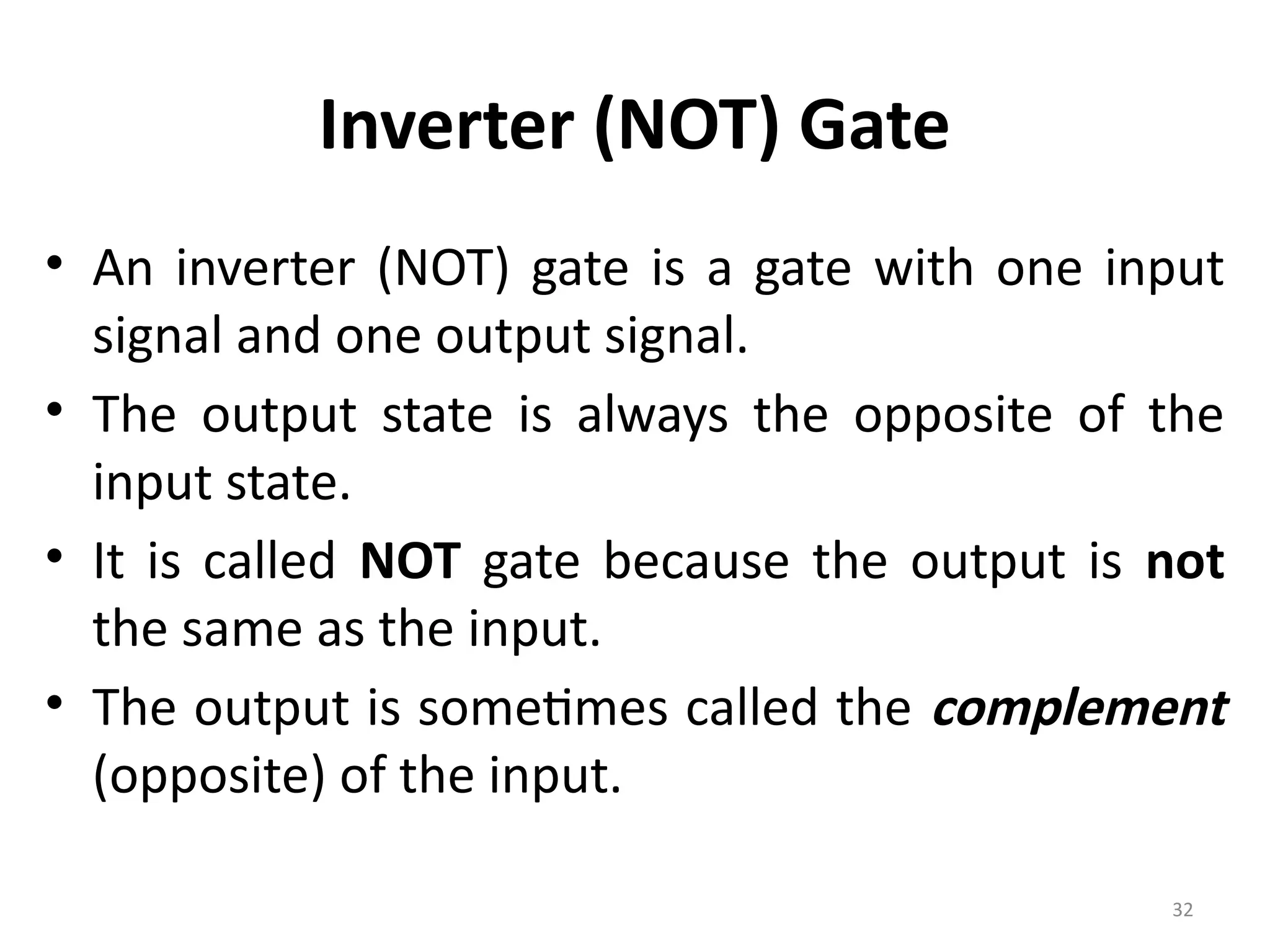
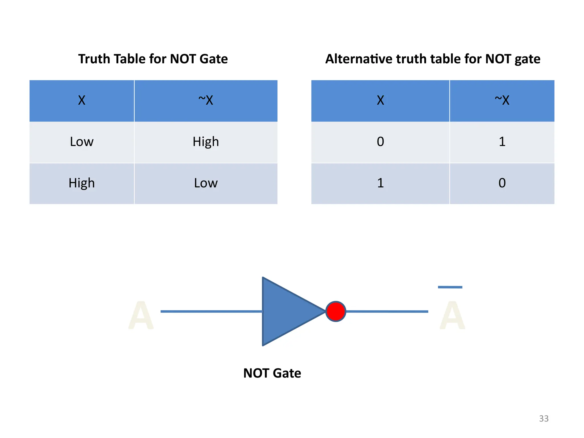
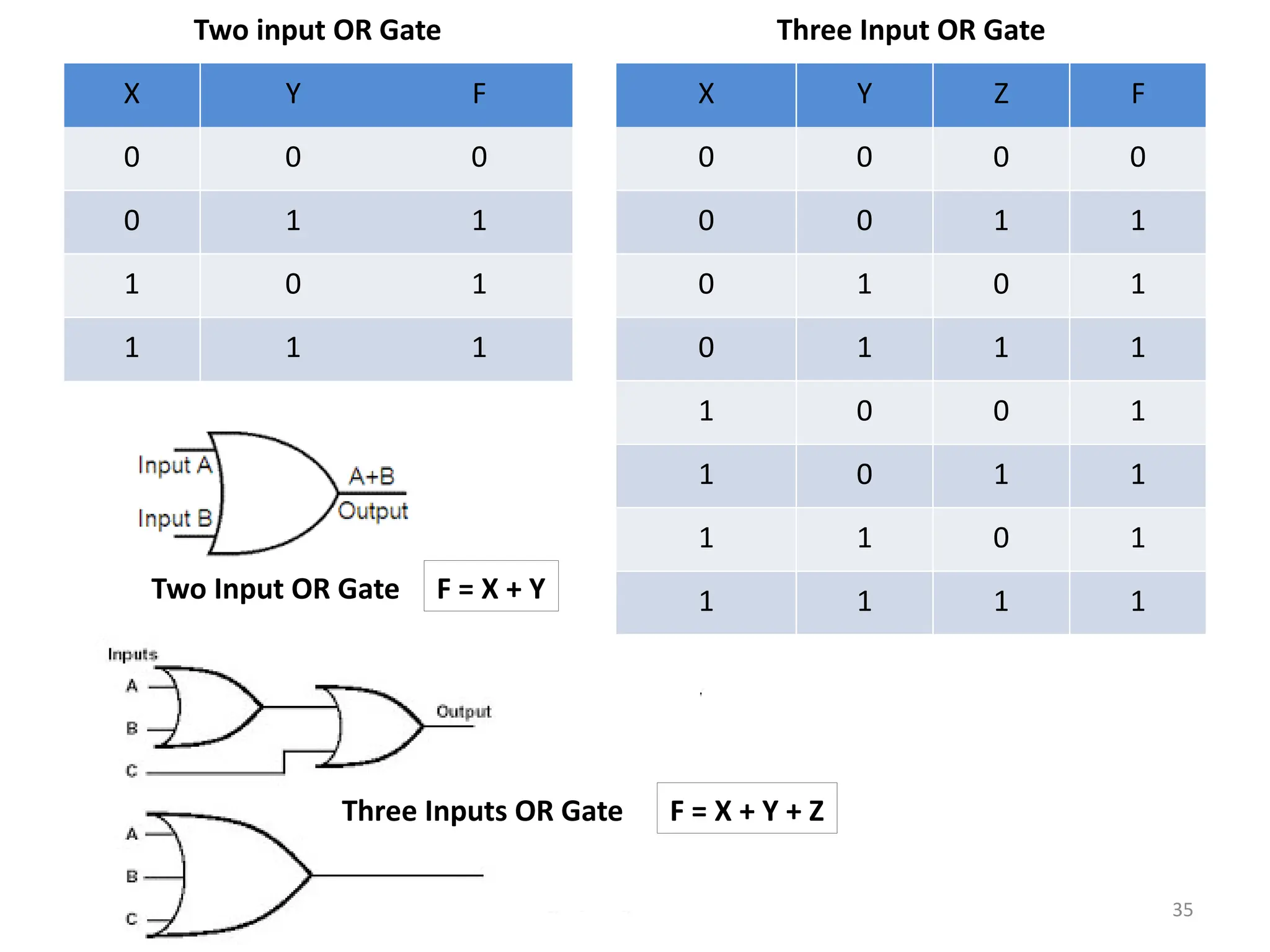
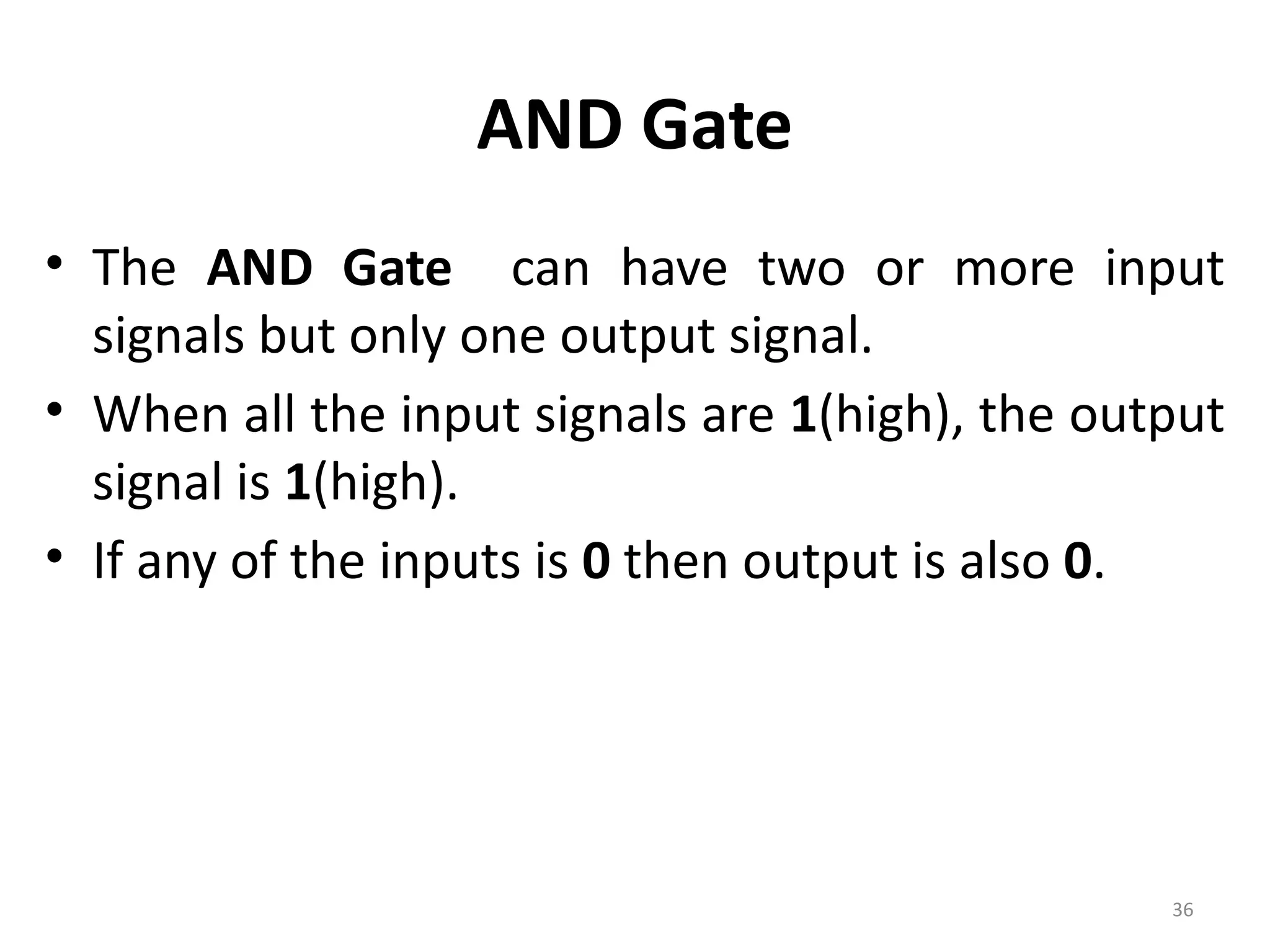
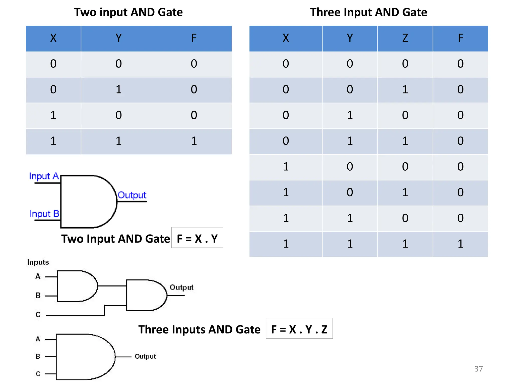
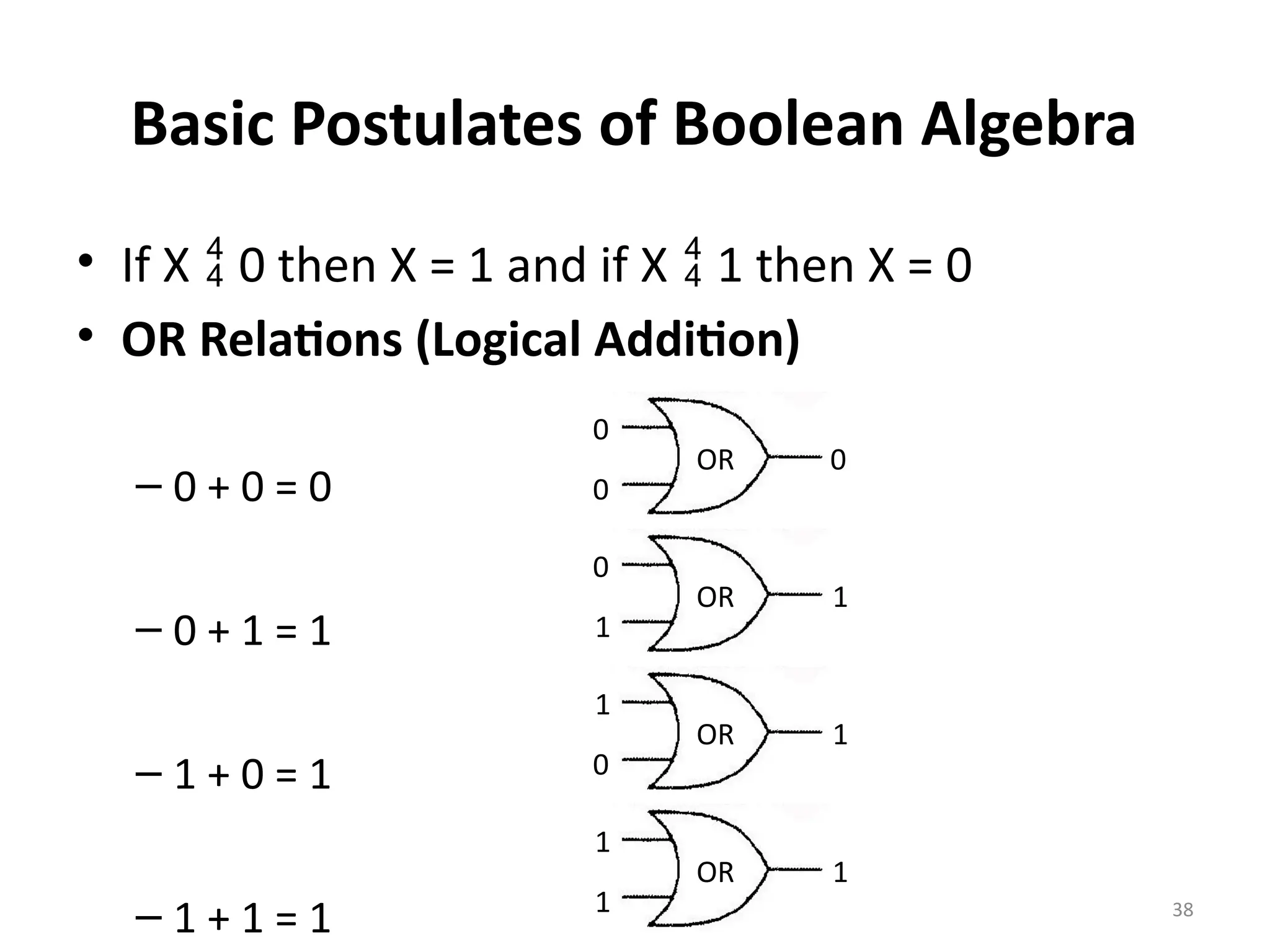
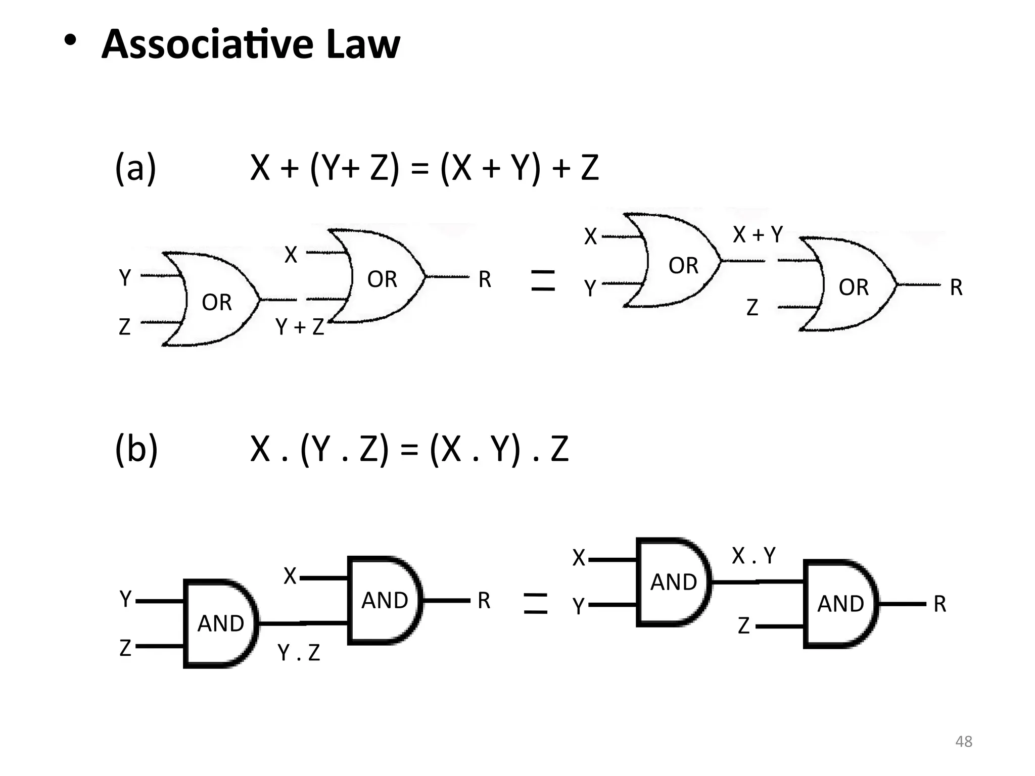
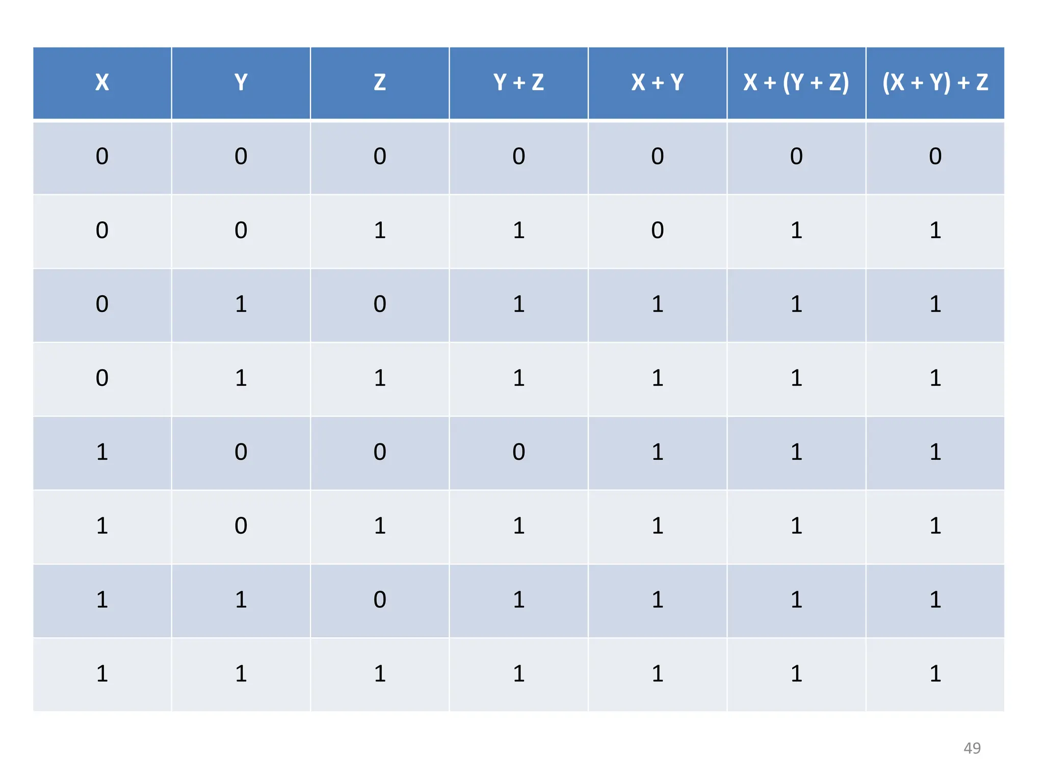
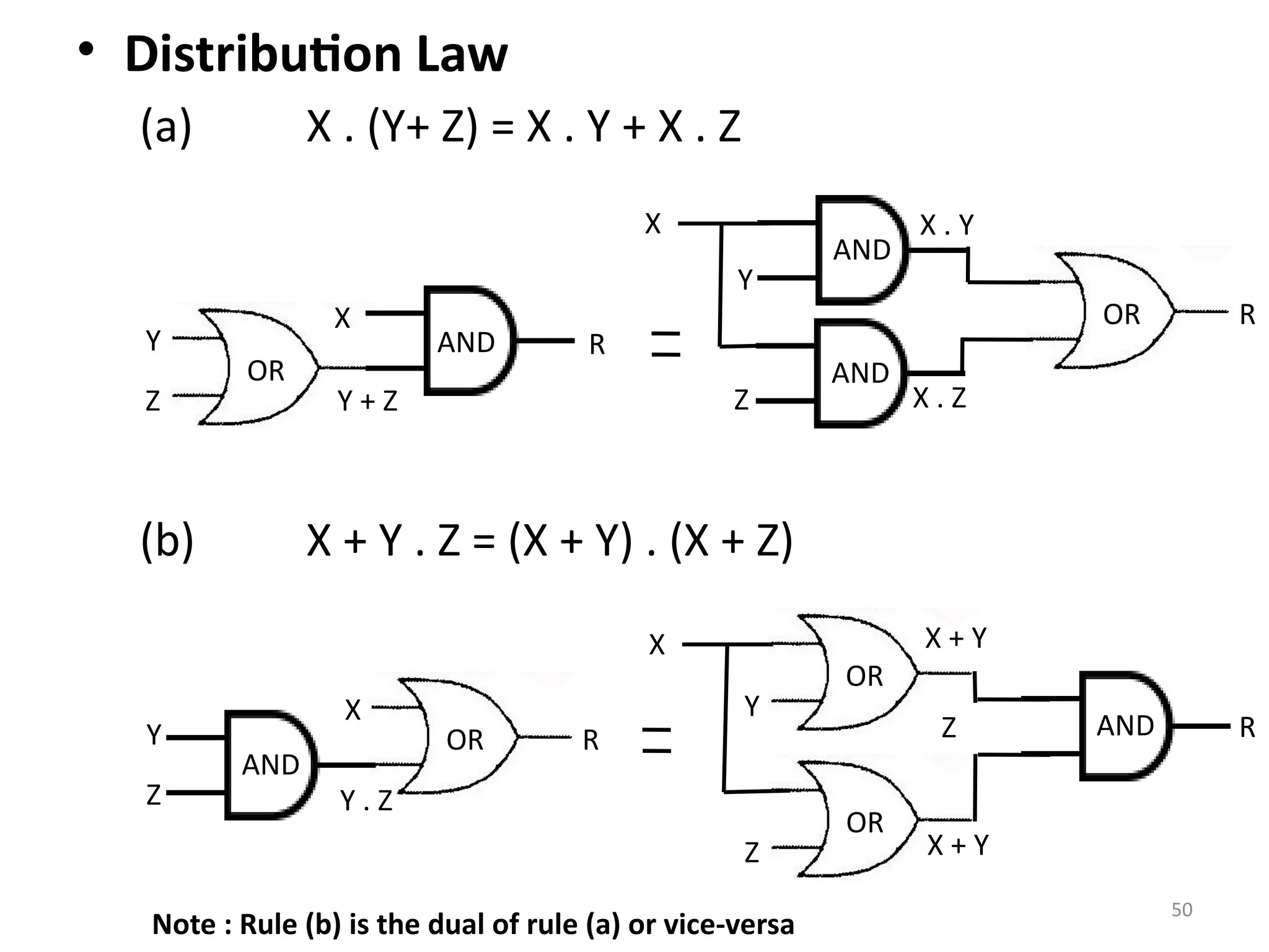
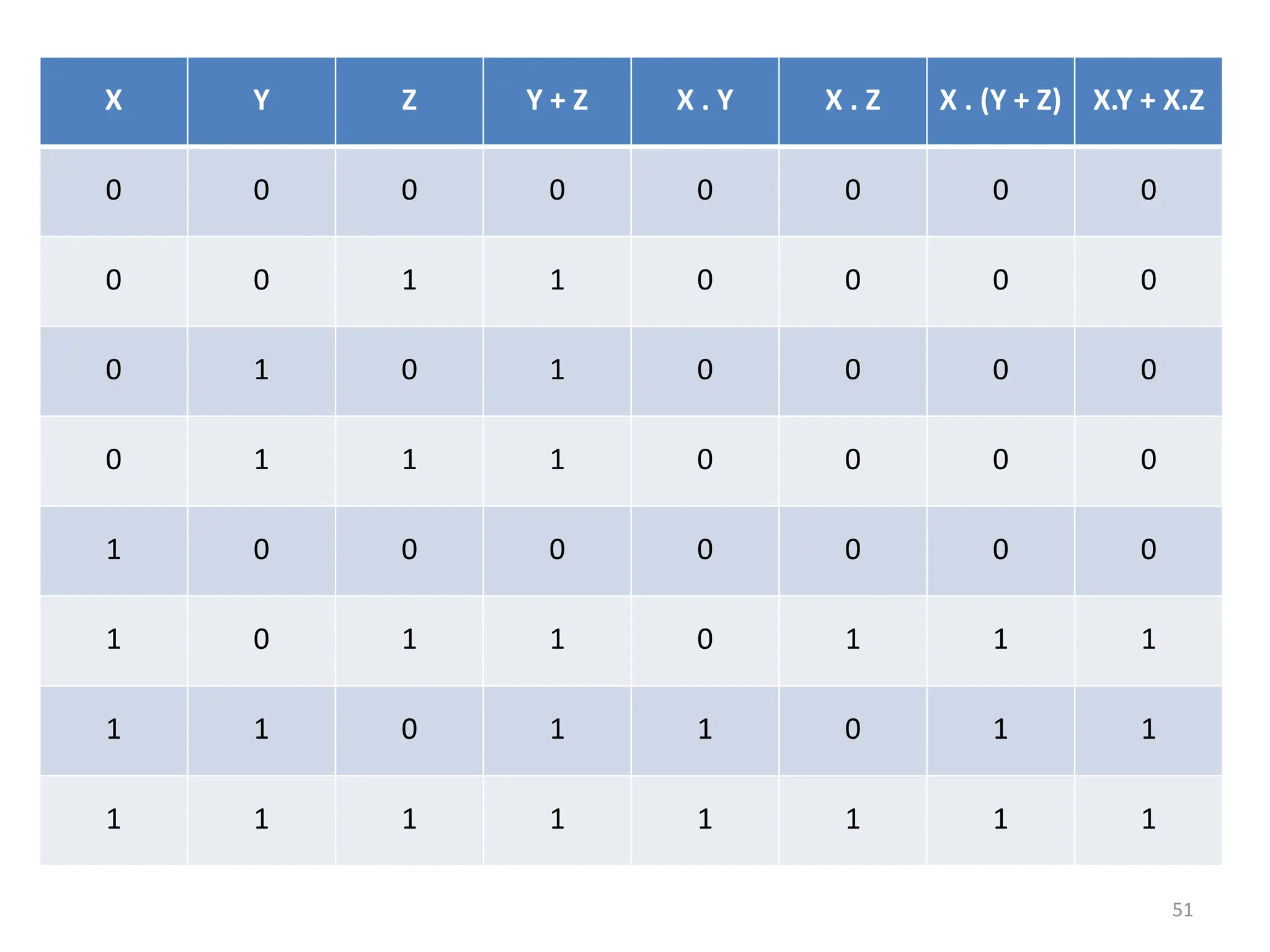
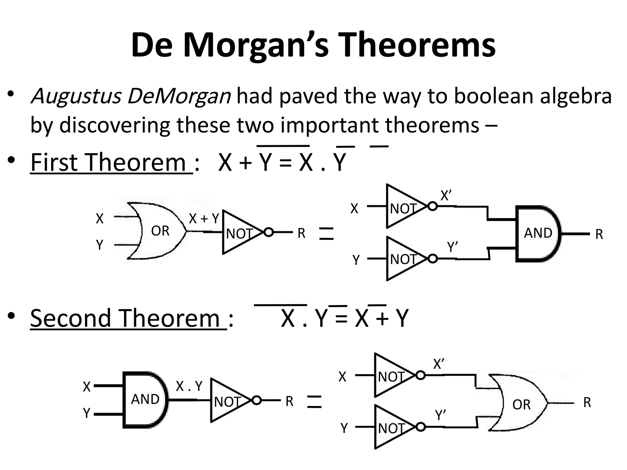
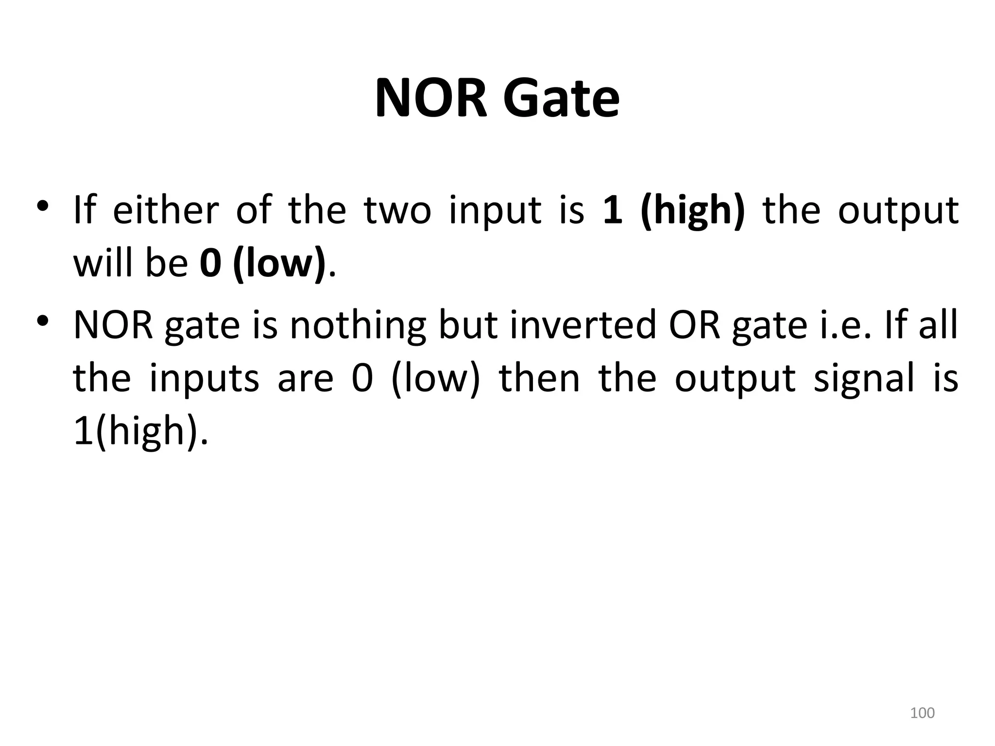
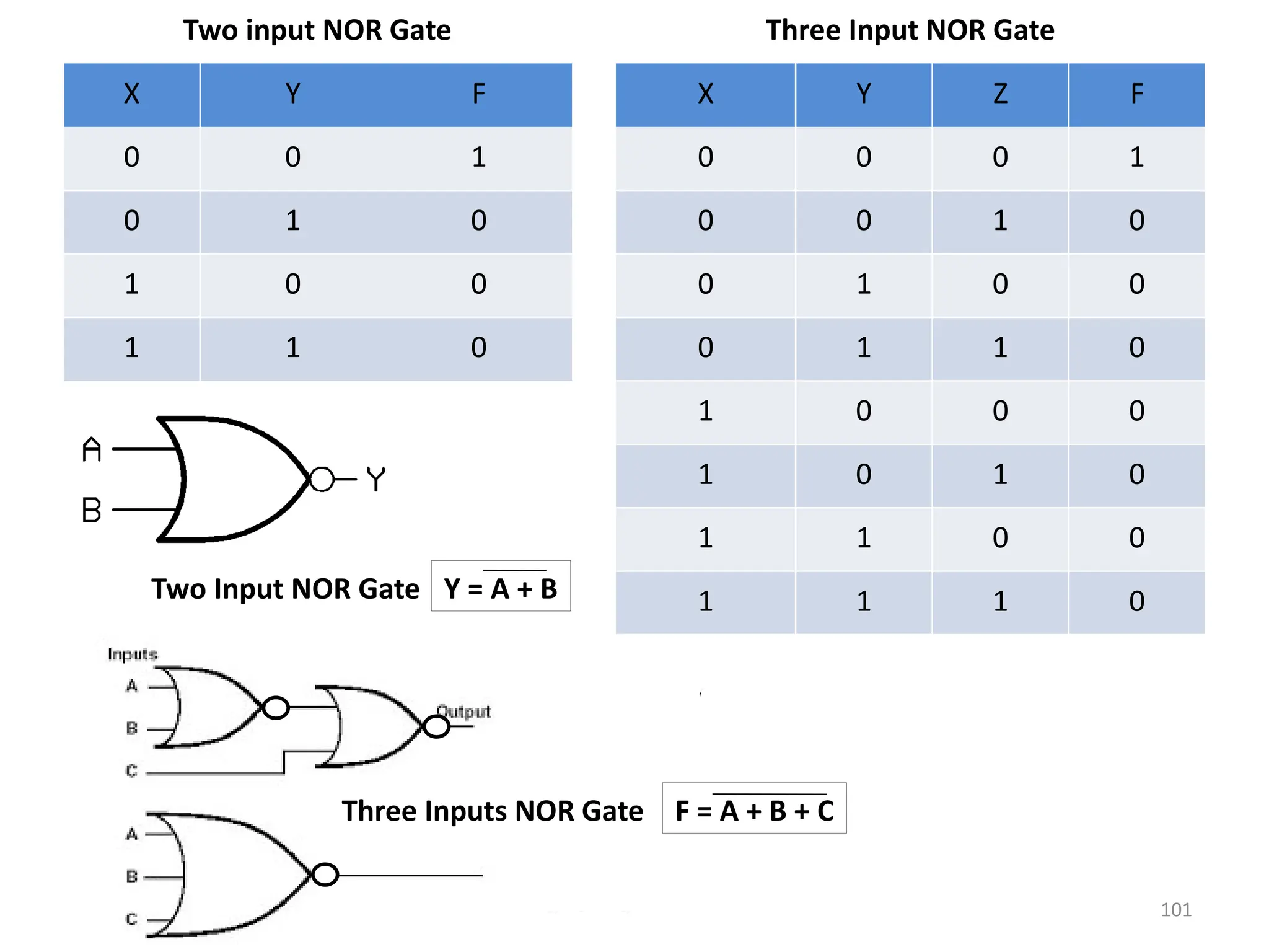
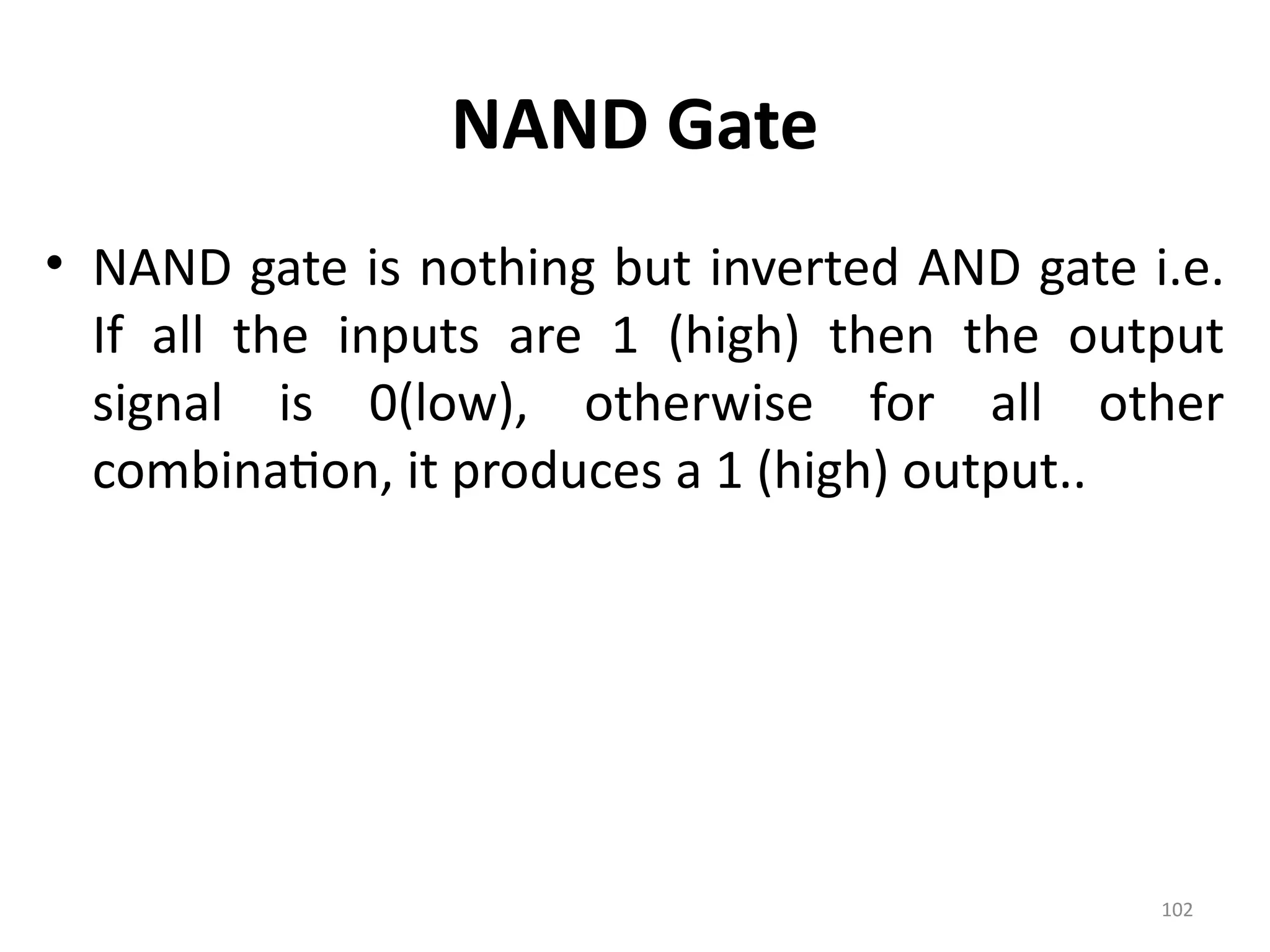
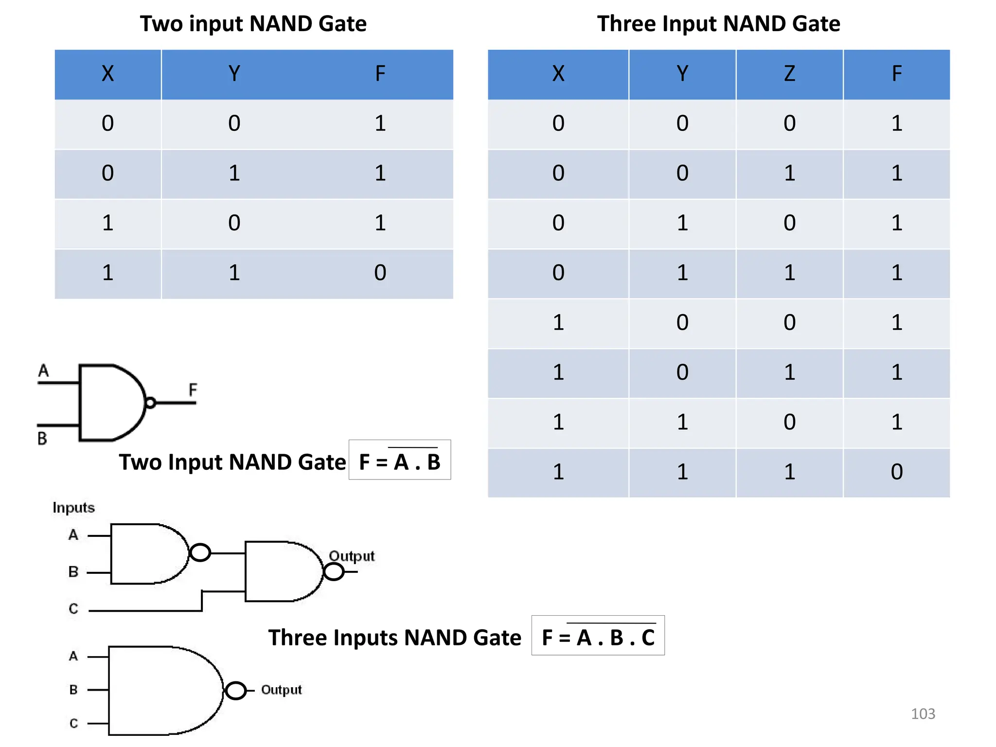
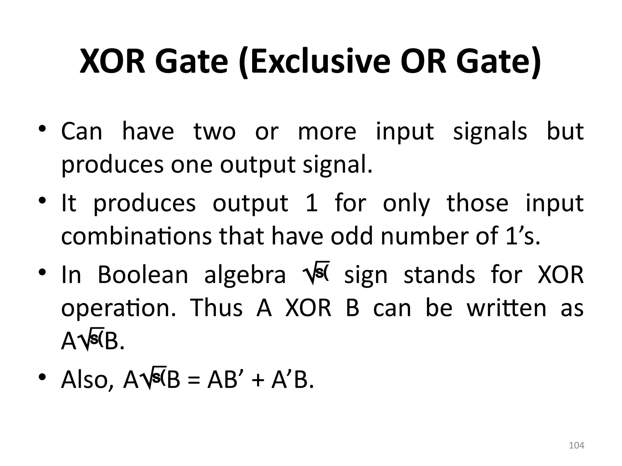
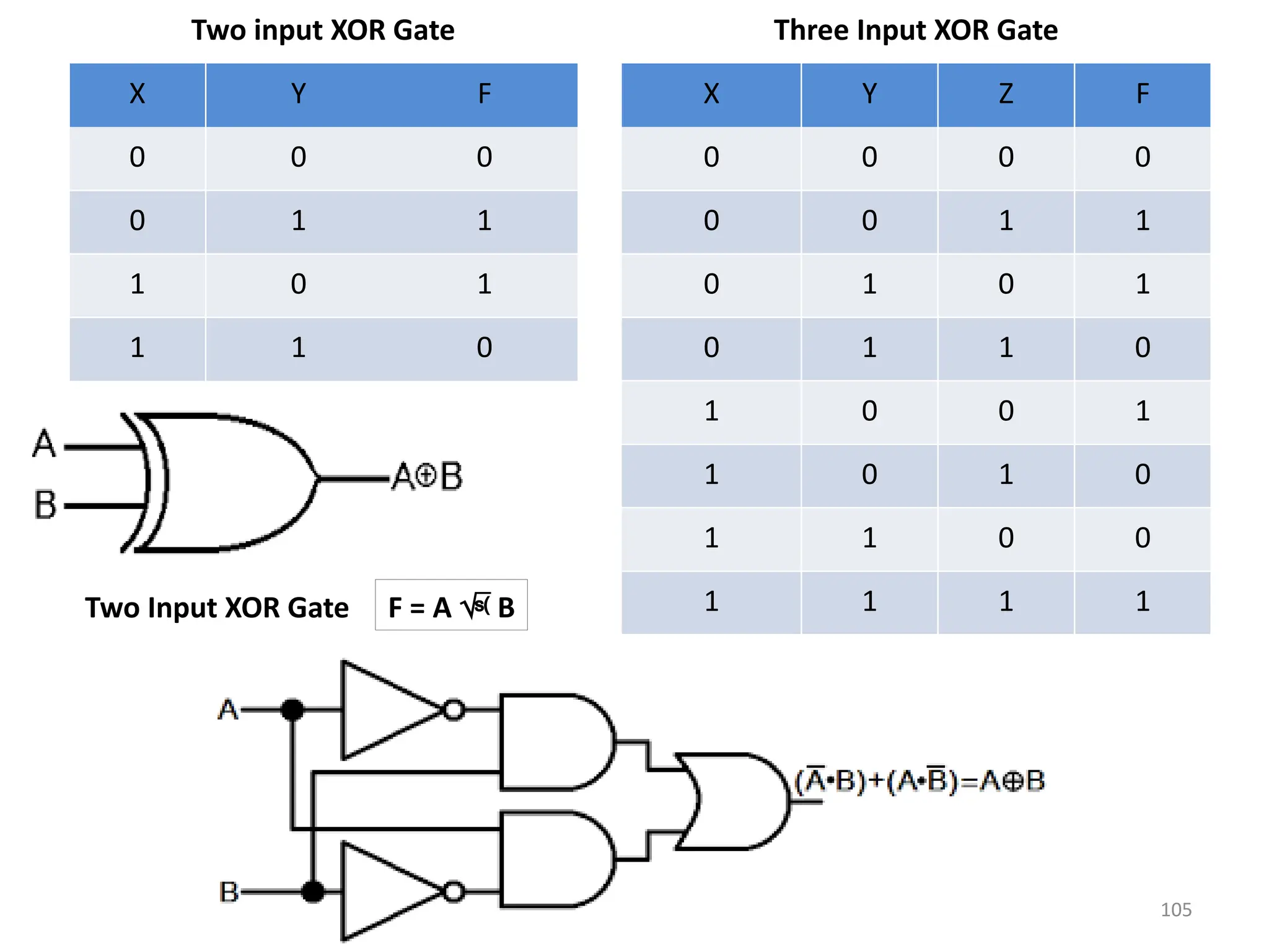
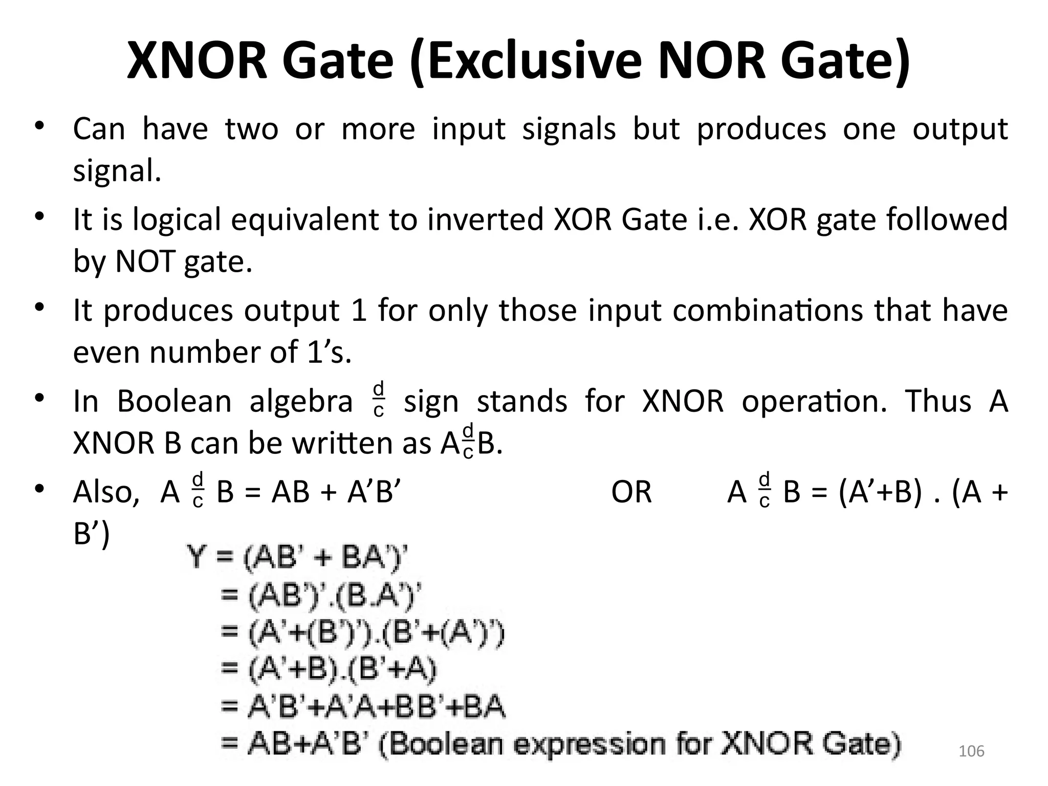
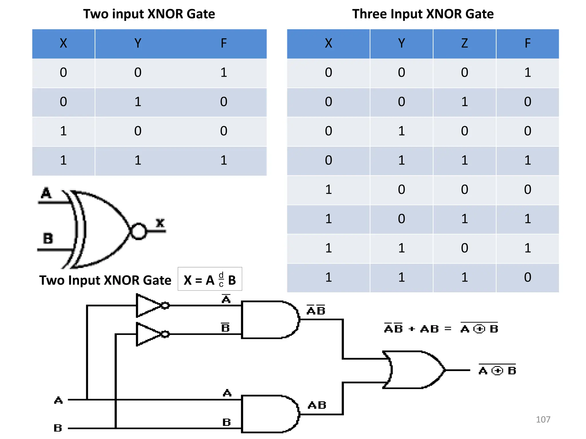
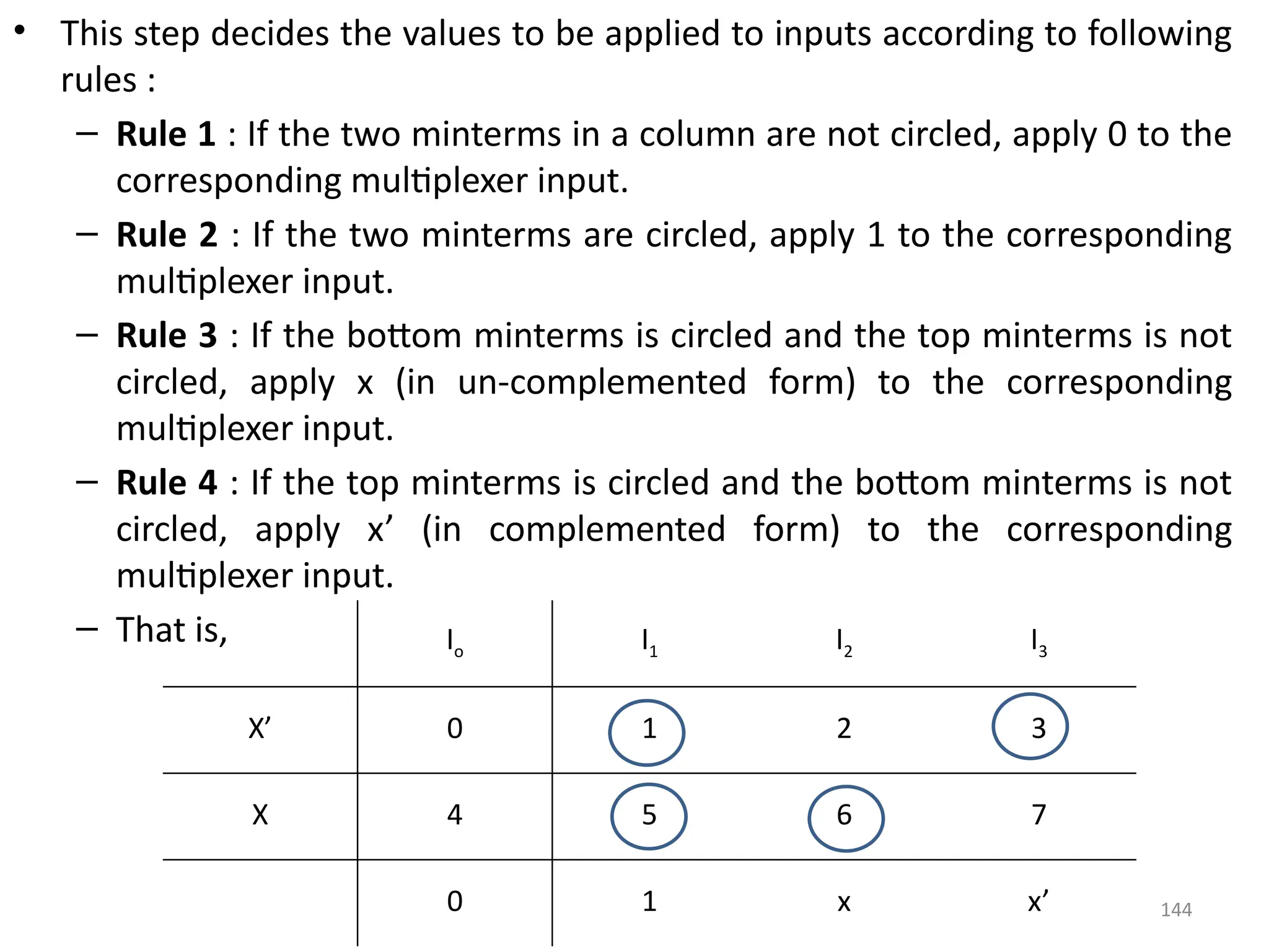
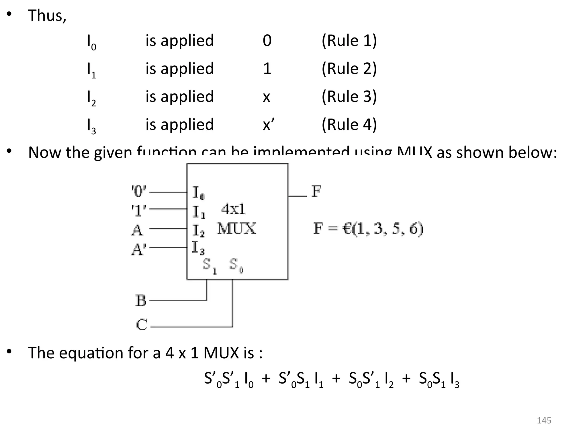
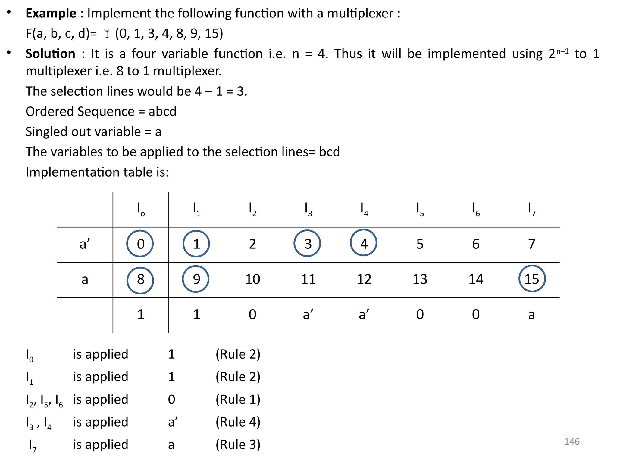
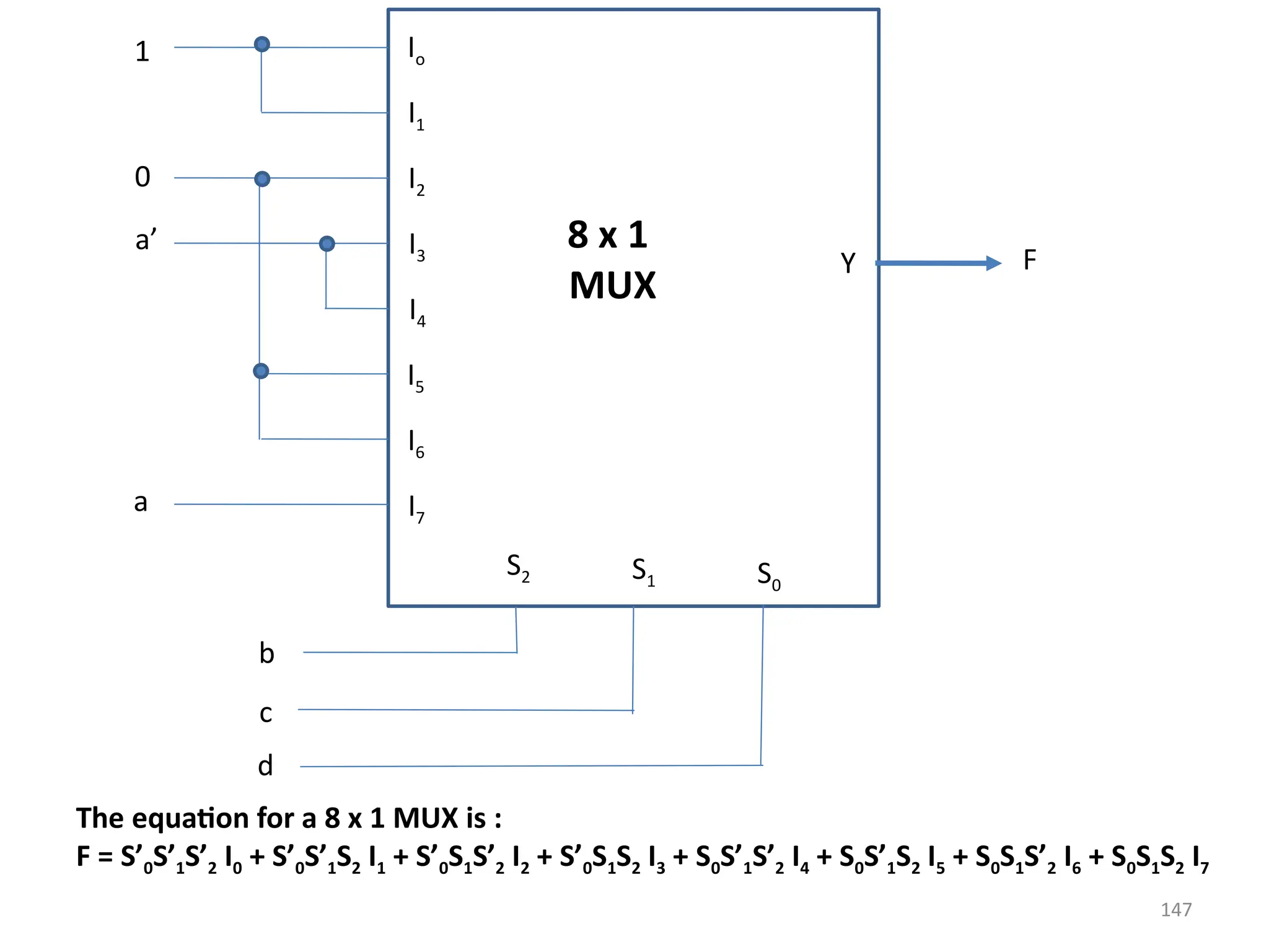
The document provides an overview of digital electronics, focusing on logical gates, boolean algebra, and propositions. It explains the types of propositions, connectives, and the truth values associated with them, detailing the characteristics of operations like conjunction, disjunction, and implications. Additionally, it covers fundamental concepts such as logic gates and principles of boolean algebra, along with their practical applications in electronic circuits.


![30
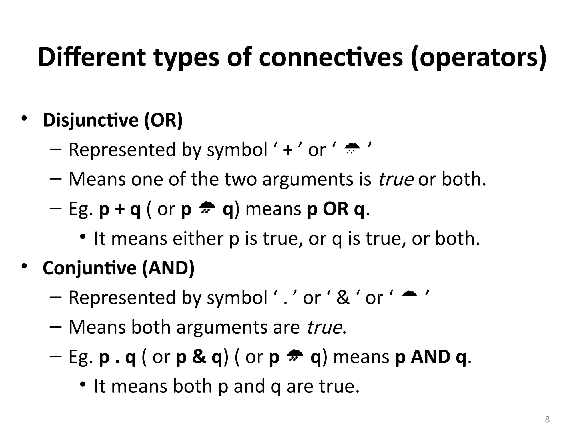
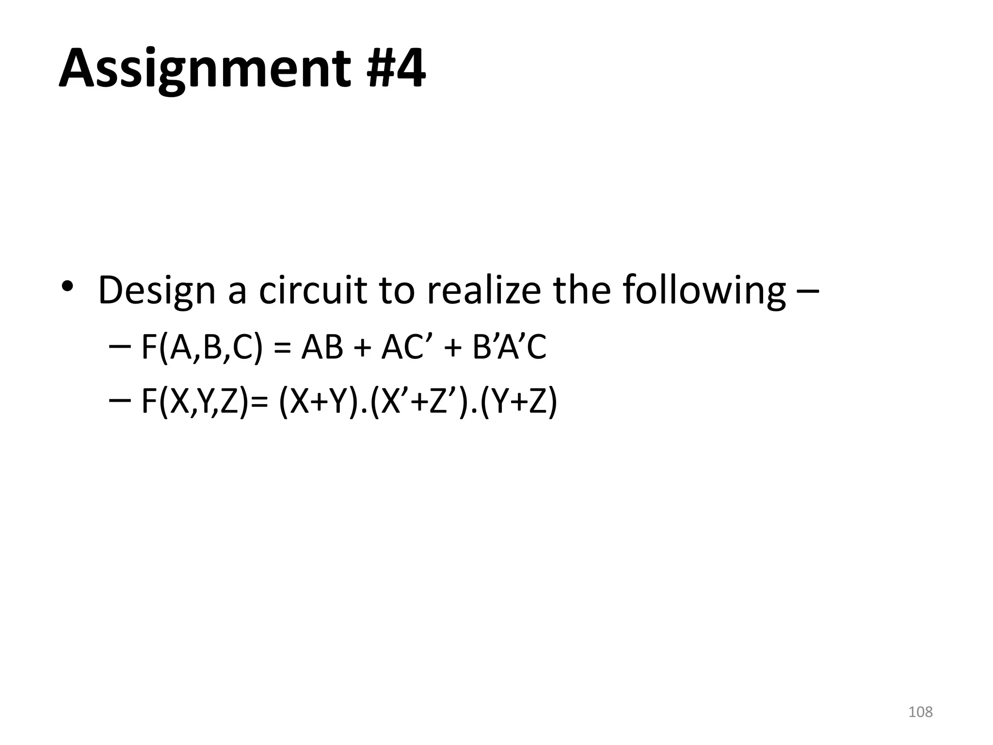
Assignment #1
• Prepare a table of combinations for the following
Boolean algebra expression:
– X + (XZ)’
– X’Y’ + X’Y
– XYZ’ + X’Y’Z
– X’YZ’ + XY’
– X(Y’ + Z’) + XY’
– XY’(Z+YZ’)+Z’
– A[(B’+C)+C’]
• Verify:
– X + XY = X
– (X + Y)’ = X’Y’](https://image.slidesharecdn.com/deupdated-240927103330-16694ebe/75/General-concepts-of-digital-electronics-and-30-2048.jpg)

![61
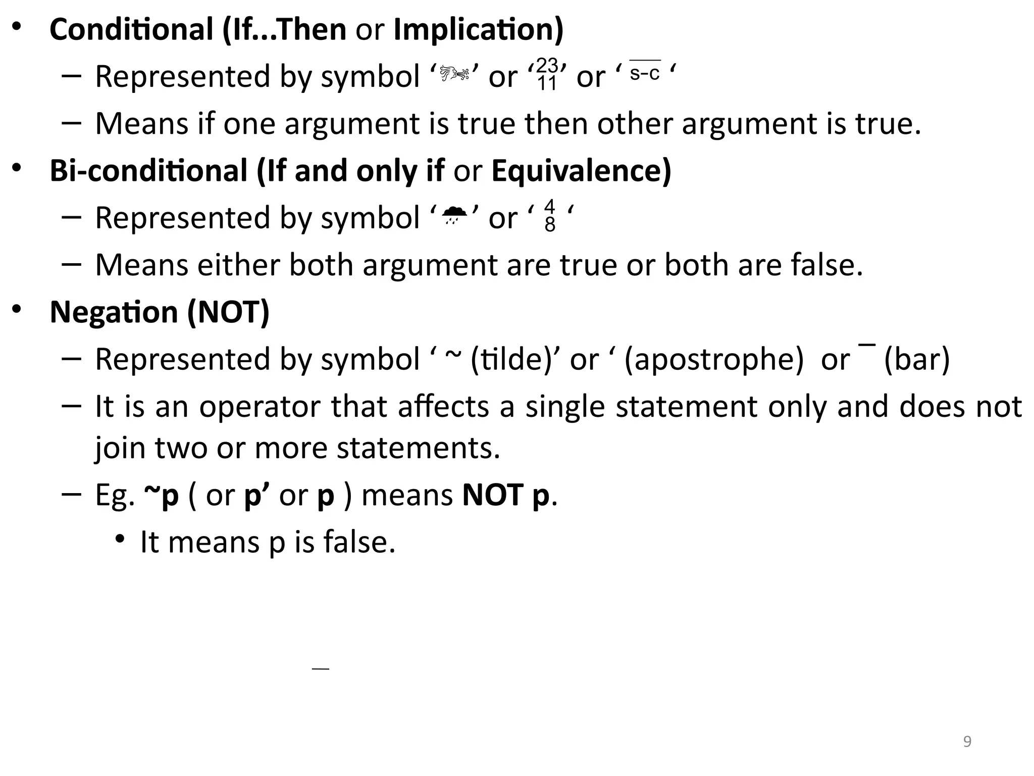
Assignment #2
• Prepare truth table for the following boolean algebra expressions –
(a) X (Y’ + Z’) + XY’ (b) XY’ (Z + YZ’) + Z’ (c) A[(B’ + C) + C’]
• Give the dual of the boolean expression –
(X + Y) . (X’ + Z’) . (Y + Z)
• Select the boolean expression that is not equivalent to : x . x + x . x’
(a) x . (x + x’) (b) (x + x’) . x (c) x’ (d) x
• Select the boolean expression that is equivalent to: (x + y) . (x + y’)
(a) y (b) y’ (c) x (d) x’
• Which of the following relationships represents the dual of the Boolean property:
x + x’y = x + y
(a) x’ (x + y’) = x’y’ (b) x(x’y) = xy (c) x.x’ + y = xy (d) x’ (xy’) = x’y’
(e) x (x’ + y) = xy
• Give duals for the following –
(a) X + X’Y (b) XY + XY’ + X’Y (c) (A + 0).(A . 1 . A’) (d) AB + A’B
(e) ABC + AB’C + A’BC’
• Find the complement of the following boolean function –
AB’ + C’D’
• Find the complement of F = x + yz; then show that F.F’ = 0 and F+F’ = 1
• Using DeMorgan’s Theorem, convert the following Boolean expressions to equivalent
expressions that have only OR and complement operations –
(a) F = x’y’ + x’z + y’z (b) F = (y + z’) (x + y) (y’ + z)](https://image.slidesharecdn.com/deupdated-240927103330-16694ebe/75/General-concepts-of-digital-electronics-and-61-2048.jpg)
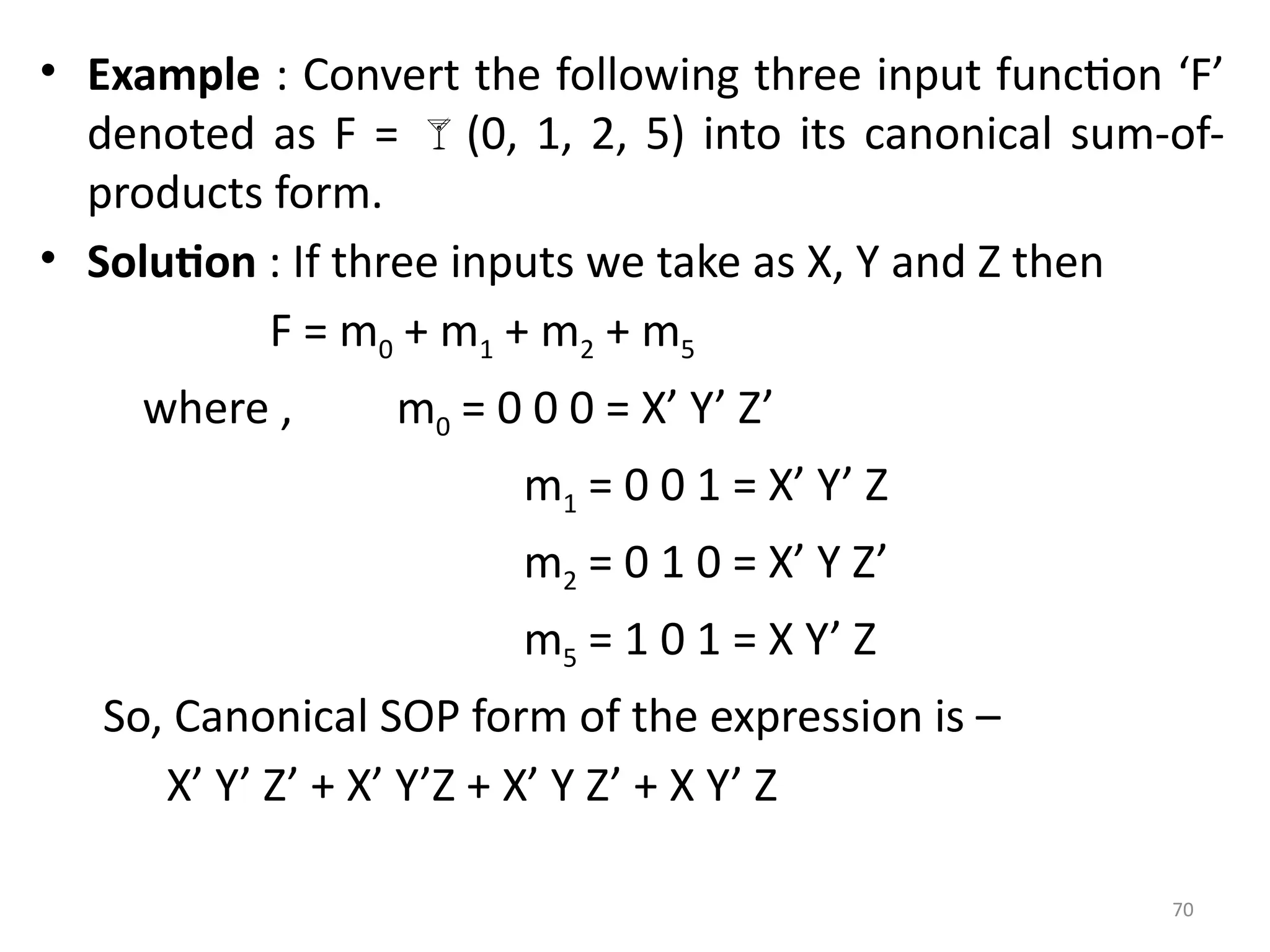
![69
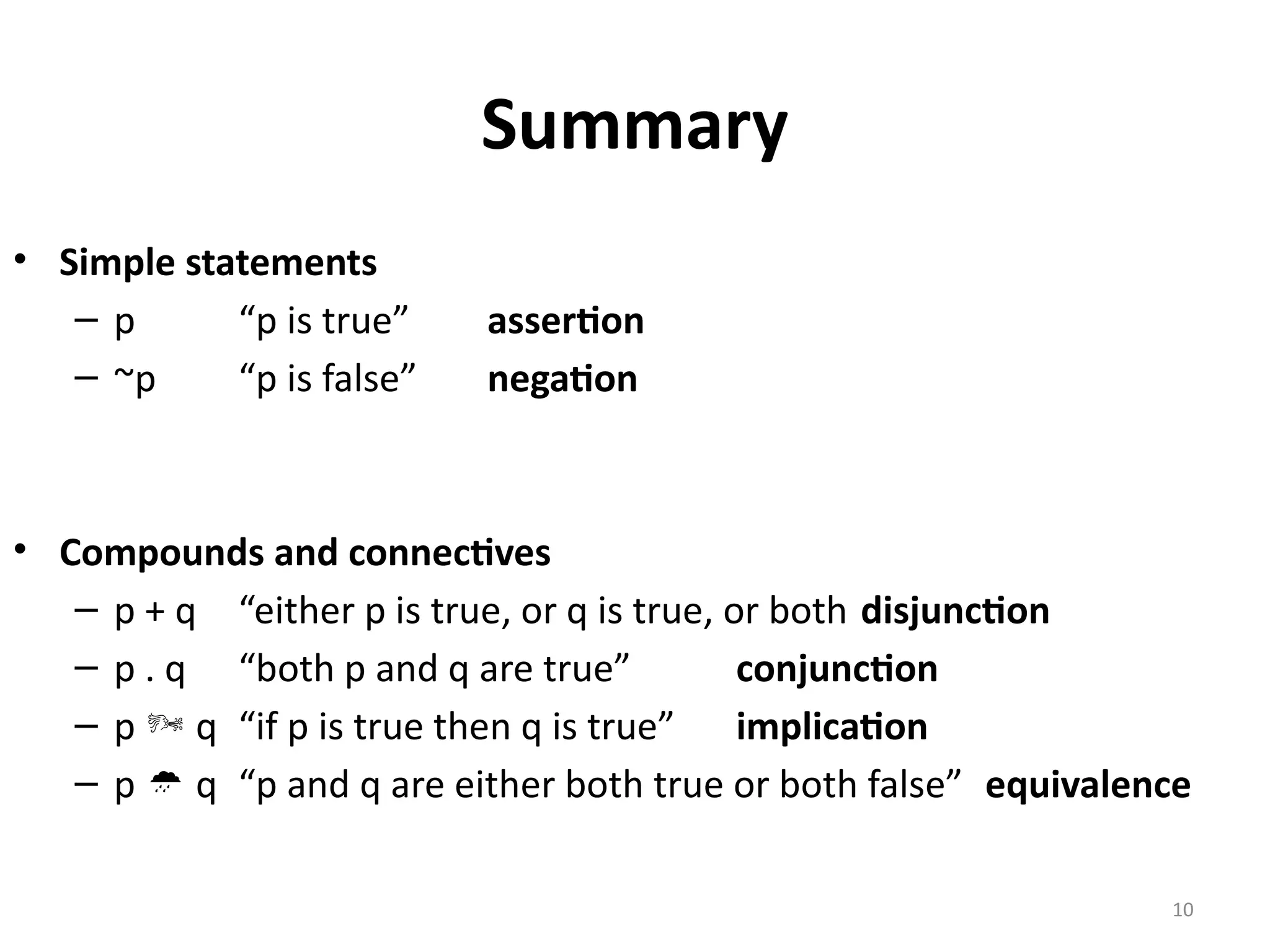
Example : Convert [(X’Y) + (X’Z’)]’ into canonical sum of product form.
Solution :
• Rule 1 : Simplify the given expression using appropriate theorem/rules :
[(X’Y) + (X’Z’)]’ = (X + Y’) (X + Z) (using Demorgans Theorem)
= X + Y’Z [X + YZ = (X+Y).(X+Z)]
Since it is a 3 variable expression, a product term must have all 3 variables.
• Rule 2 : Wherever a literal is missing, multiply that term with missing term +
complement of missing term) factor, i.e.
= X + Y’Z
= X(Y+Y’)(Z+Z’) + (X+X’)Y’Z
= (XY + XY’)(Z+Z’) + (X+X’)Y’Z
= XYZ + XYZ’ + XY’Z + XY’Z’ + XY’Z + X’Y’Z
• Rule 3 : Remove all duplicate terms i.e.
= XYZ + XY’Z + XYZ’ + XY’Z’ + X’Y’Z
This is the desired Canonical Sum-of-Products form.
– Above SOP expression can also be represented by following shorthand notation i.e.
F = (1, 4, 5, 6, 7) or F = m(1, 4, 5, 6, 7)
where, ‘F’ is a variable function and ‘m’ is a notation for minterm.
i.e. F = m1 + m4 + m5 + m6 + m7](https://image.slidesharecdn.com/deupdated-240927103330-16694ebe/75/General-concepts-of-digital-electronics-and-69-2048.jpg)
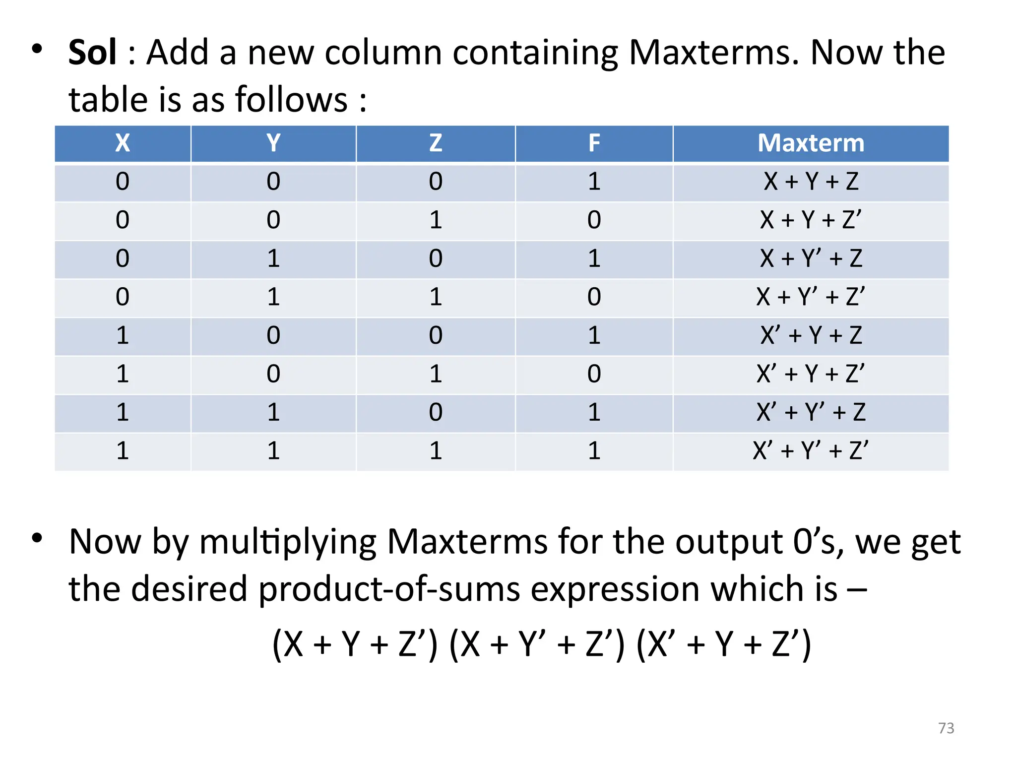
![74
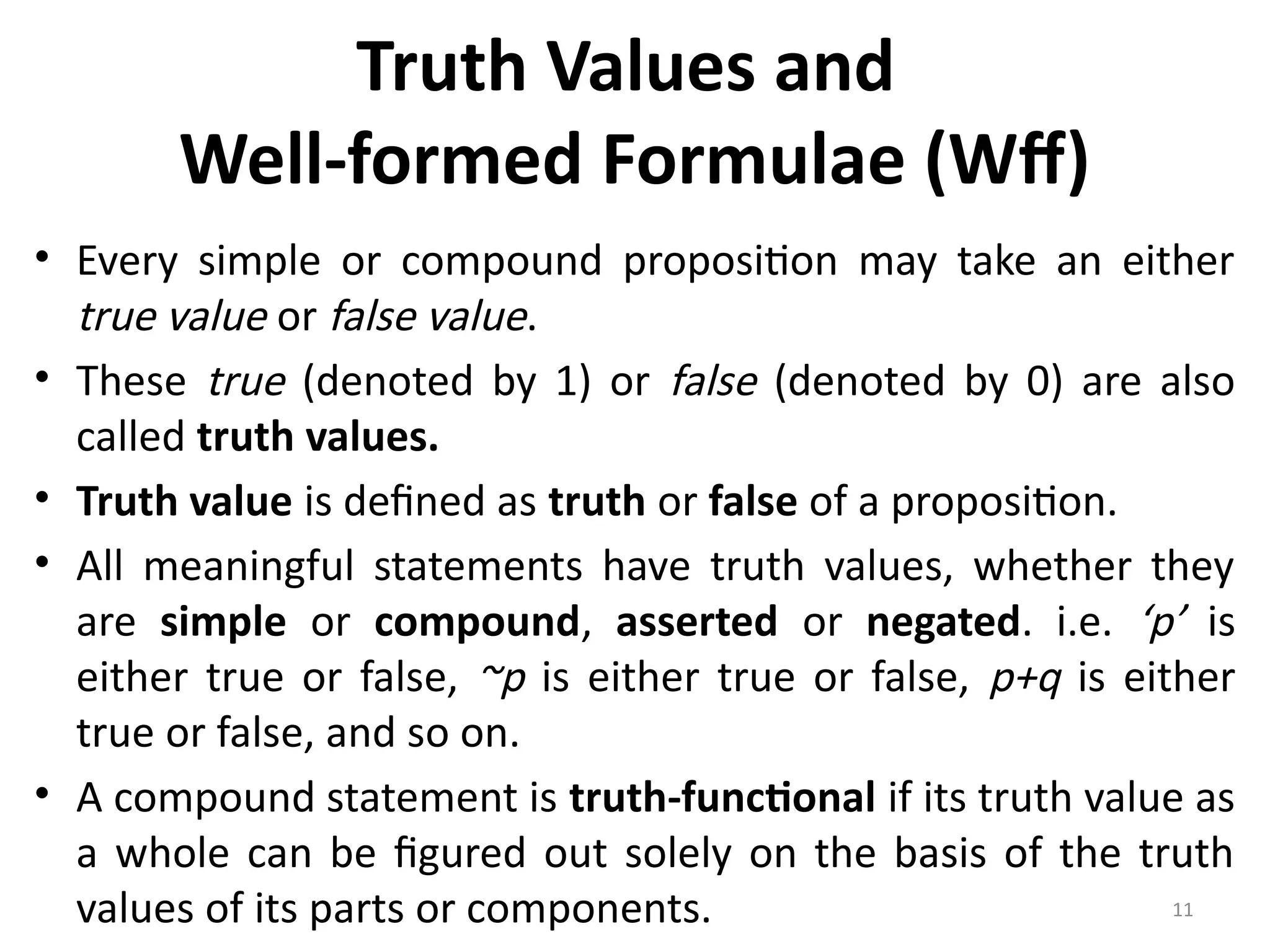
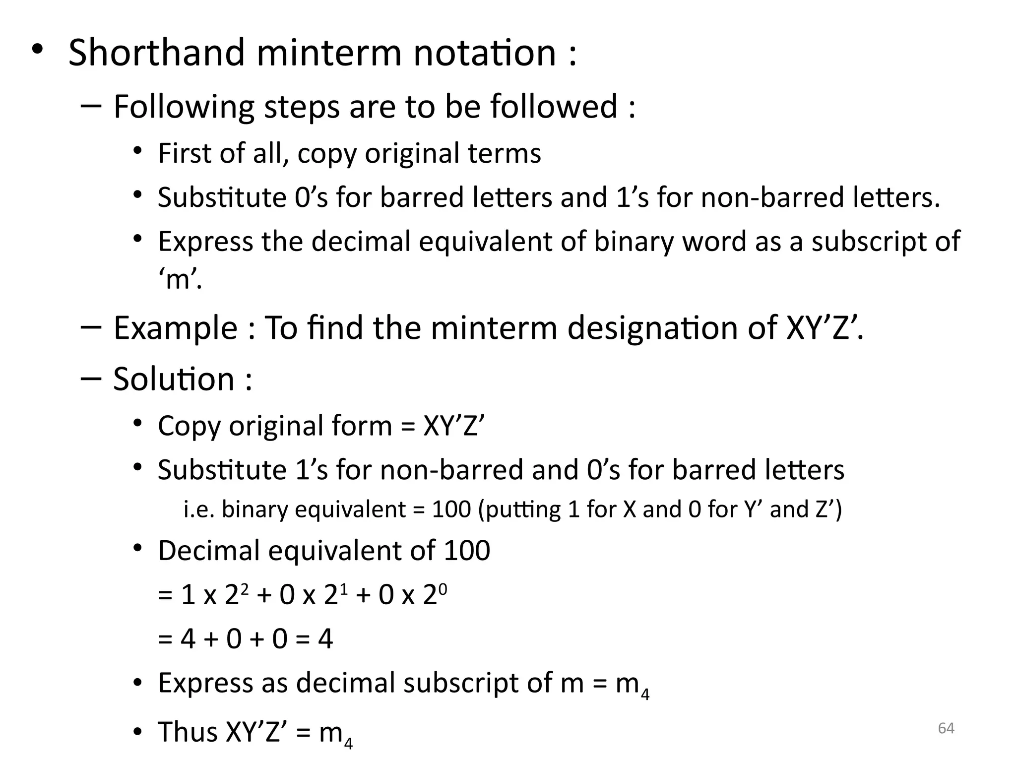
• Express X’Y + Y(Z’(Z’ + Y)) into canonical product-of-sums form.
• Rule 1 : Simplify the given expression using appropriate theorems/rules.
X’Y + Y(Z’(Z’ + Y)) = X’Y + Y(Z’Z’ + YZ’)
= X’Y + Y(Z’ + YZ’)
= X’Y + Y.Z’(1 + Y)
= X’Y + YZ’.1
= X’Y + YZ’
• Rule 2 : To convert into product of sums form, apply the boolean algebra rule which states that
X + YZ = (X + Y) . (X + Z)
• Now applying this rule we get,
X’Y + YZ’ = (X’Y + Y).(X’Y + Z’)
= (Y + X’Y).(Z’ + X’Y)
= (Y + X’) . (Y + Y) . (Z’ + X’) . (Z’ + Y)
= (X’ + Y) . (Y) . (X’ + Z’) . (Y + Z’)
• Now, this is in product of sums form but not in canonical product of sums form (in canonical
expression all the sum terms are Maxterms).
• Rule 3 : After converting into product of sum terms, in a sum term for missing variable add
[(missing variable ). (complement of missing variable)] e.g. if variable Y is missing then add Y.Y’
i.e. (X’ + Y) . (Y) . (X’ + Z’) . (Y + Z’)
• Terms 1 2 3 4
= (X’ + Y + ZZ’) . (XX’ + Y + ZZ’) . (X’ + YY’ + Z’) . (XX’ + Y + Z’)](https://image.slidesharecdn.com/deupdated-240927103330-16694ebe/75/General-concepts-of-digital-electronics-and-74-2048.jpg)
![79
Y
X
[0] Y’ [1] Y
[0] X’ X’Y’
0
X’Y
1
[1] X XY’
2
XY
3
Y
X
[0] Y’ [1] Y
[0] X’
0 1
[1] X
2 3
YZ
X
[00] Y’Z’ [01] Y’Z [11]YZ [10]YZ’
[0] X’ X’Y’Z’
0
X’Y’Z
1
X’YZ
3
X’YZ’
2
[1] X XY’Z’
4
XY’Z
5
XYZ
7
XYZ’
6
YZ
X
[00] Y’Z’ [01] Y’Z [11]YZ [10]YZ’
[0] X’
0 1 3 2
[1] X
4 5 7 6
2-variable K-map representing minterms 3-variable K-map representing minterms](https://image.slidesharecdn.com/deupdated-240927103330-16694ebe/75/General-concepts-of-digital-electronics-and-79-2048.jpg)
![80
YZ
WX [00] Y’Z’ [01] Y’Z [11]YZ [10]YZ’
[00] W’X’ W’X’Y’Z’
0
W’X’Y’Z
1
W’X’YZ
3
W’X’YZ’
2
[01] W’X W’XY’Z’
4
W’XY’Z
5
W’XYZ
7
W’XYZ’
6
[11] WX WXY’Z’
12
WXY’Z
13
WXYZ
15
WXYZ’
14
[10] WX’ WX’Y’Z’
8
WX’Y’Z
9
WX’YZ
11
WX’YZ’
10
YZ
WX [00] Y’Z’ [01] Y’Z [11]YZ [10]YZ’
[00] W’X’
0 1 3 2
[01] W’X
4 5 7 6
[11] WX
12 13 15 14
[10] WX’
8 9 11 10
4-variable K-map
representing minterms
The binary code 00, 01, 11, 10 is
called Gray Code. Gray Code is
the binary code in which each
successive number differs only in
one place. That is why box
numbering scheme follows above
order only.](https://image.slidesharecdn.com/deupdated-240927103330-16694ebe/75/General-concepts-of-digital-electronics-and-80-2048.jpg)
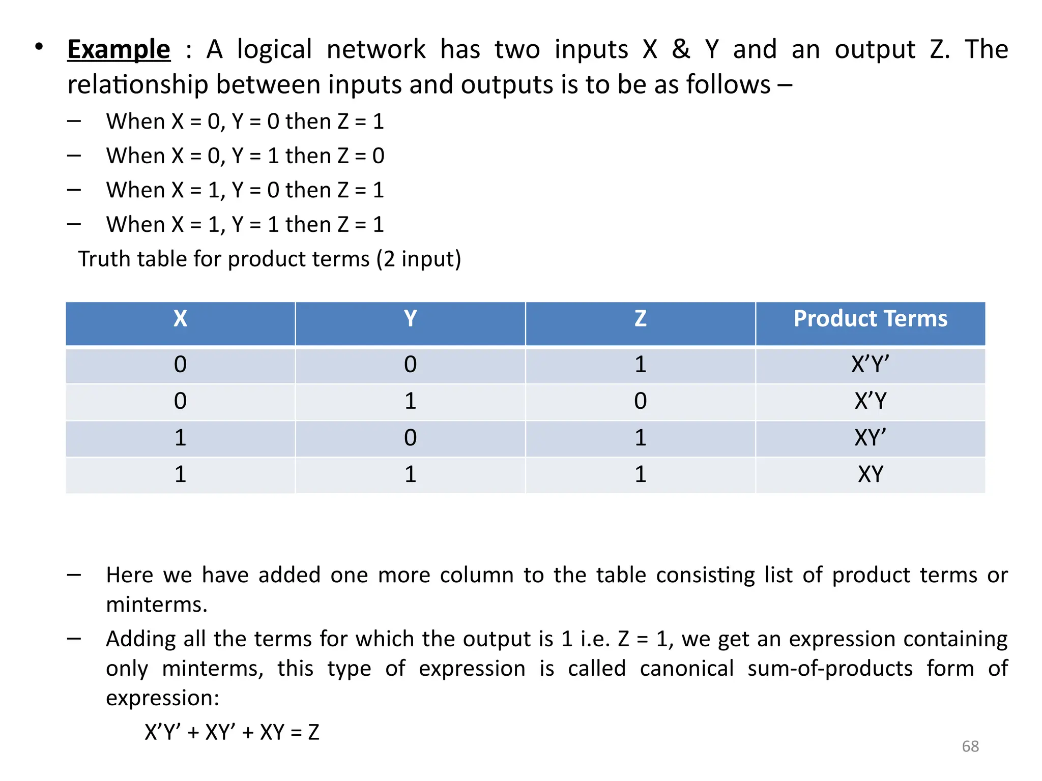
![81
• How to map in K-map?
• Suppose, we have been given with the following truth table for mapping -
• Canonical SP expression for this table is
F = AB’ + AB or F = (2, 3)
• The blank K-map for 2-variable will be
• For minterm m2 and m3 the output is 1. Thus, mark 1 in the squares for m2 and m3 i.e. square
numbered as 2 and 3.
• After entering 1’s for all ‘1’ output, enter 0’s in all blank squares. The K-map will now look like as –
• Same is the method for mapping 3-variable, 4-variable etc.
A B F
0 0 0
0 1 0
1 0 1
1 1 1
B
A
[0] B’ [1] B
[0] A’ 0 1
[1] A 2 3
B
A
[0] B’ [1] B
[0] A’ 0 0
[1] A 1 1](https://image.slidesharecdn.com/deupdated-240927103330-16694ebe/75/General-concepts-of-digital-electronics-and-81-2048.jpg)
![83
• Reduction of a Pair –
• In the K-map shown below, after mapping a
given function F(W, X, Y Z) two pairs have been
marked. Pair-1 is m0 + m4 (group of 0th
minterm
and 4th
minterm). Pair-2 is m14 + m15.
YZ
WX [00] Y’Z’ [01] Y’Z [11]YZ [10]YZ’
[00] W’X’ 1
0
0
1
0
3
0
2
[01] W’X 1
4
0
5
0
7
0
6
[11] WX 0
12
0
13
1
15
1
14
[10] WX’ 0
8
0
9
0
11
0
10](https://image.slidesharecdn.com/deupdated-240927103330-16694ebe/75/General-concepts-of-digital-electronics-and-83-2048.jpg)
![85
• Reduction of a Quad –
• In the K-map shown below, after mapping a
given function F(W, X, Y Z) two quads have been
marked. Quad-1 is m0+m4+m12+m8 and Quad-2 is
m7+m6+m15+m14.
YZ
WX [00] Y’Z’ [01] Y’Z [11]YZ [10]YZ’
[00] W’X’ 1
0
0
1
0
3
0
2
[01] W’X 1
4
0
5
1
7
1
6
[11] WX 1
12
0
13
1
15
1
14
[10] WX’ 1
8
0
9
0
11
0
10](https://image.slidesharecdn.com/deupdated-240927103330-16694ebe/75/General-concepts-of-digital-electronics-and-85-2048.jpg)
![87
• Reduction of an Octect –
• Suppose we have K-map with an octet marked as
shown below -
YZ
WX [00] Y’Z’ [01] Y’Z [11]YZ [10]YZ’
[00] W’X’ 0
0
0
1
0
3
0
2
[01] W’X 0
4
0
5
0
7
0
6
[11] WX 1
12
1
13
1
15
1
14
[10] WX’ 1
8
1
9
1
11
1
10](https://image.slidesharecdn.com/deupdated-240927103330-16694ebe/75/General-concepts-of-digital-electronics-and-87-2048.jpg)

![90
YZ
WX [00] Y’Z’ [01] Y’Z [11]YZ [10]YZ’
[00] W’X’
0 1
1
3 2
[01] W’X 1
4 5 7
1
6
[11] WX
12 13 15 14
[10] WX’
8 9
1
11 10
YZ
WX [00] Y’Z’ [01] Y’Z [11]YZ [10]YZ’
[00] W’X’
0
1
1
1
3 2
[01] W’X 1
4 5 7
1
6
[11] WX 1
12 13 15
1
14
[10] WX’
8
1
9
1
11 10](https://image.slidesharecdn.com/deupdated-240927103330-16694ebe/75/General-concepts-of-digital-electronics-and-90-2048.jpg)
![91
YZ
WX [00] Y’Z’ [01] Y’Z [11]YZ [10]YZ’
[00] W’X’ 1
0 1 3
1
2
[01] W’X
4 5 7 6
[11] WX
12 13 15 14
[10] WX’ 1
8 9 11
1
10
YZ
WX [00] Y’Z’ [01] Y’Z [11]YZ [10]YZ’
[00] W’X’ 1
0
1
1
1
3
1
2
[01] W’X
4 5 7 6
[11] WX
12 13 15 14
[10] WX’ 1
8
1
9
1
11
1
10](https://image.slidesharecdn.com/deupdated-240927103330-16694ebe/75/General-concepts-of-digital-electronics-and-91-2048.jpg)
![92
• Overlapping Groups
– Overlapping means same ‘1’ can be encircled
more than once.
– For eg. consider the following K-map -
YZ
WX
[00] Y’Z’ [01] Y’Z [11]YZ [10]YZ’
[00] W’X’
0 1 3 2
[01] W’X
4
1
5
1
7
1
6
[11] WX
12 13
1
15
1
14
[10] WX’
8 9 11
1
10](https://image.slidesharecdn.com/deupdated-240927103330-16694ebe/75/General-concepts-of-digital-electronics-and-92-2048.jpg)
![• Redundant Groups
– Redundant group is a group whose all 1’s are overlapped by
other groups (i.e. pairs, quads, octets).
– Redundant groups must be removed.
– For eg. consider the following K-map –
with redundant group without redundant group
94
YZ
WX
[00] Y’Z’ [01] Y’Z [11]YZ [10]YZ’
[00] W’X’
0 1 3 2
[01] W’X 1
4
1
5 7 6
[11] WX
12
1
13
1
15 14
[10] WX’
8 9 11 10
YZ
WX
[00] Y’Z’ [01] Y’Z [11]YZ [10]YZ’
[00] W’X’
0 1 3 2
[01] W’X 1
4
1
5 7 6
[11] WX
12
1
13
1
15 14
[10] WX’
8 9 11 10](https://image.slidesharecdn.com/deupdated-240927103330-16694ebe/75/General-concepts-of-digital-electronics-and-94-2048.jpg)
![97
Y
X
[0] Y [1] Y’
[0] X X+Y
0
X+Y’
1
[1] X’ X’+Y
2
X’+Y’
3
Y
X
[0] Y [1] Y’
[0] X
0 1
[1] X’
2 3
YZ
X
[00] Y+Z [01] Y+Z’ [11]Y’+Z’ [10]Y’+Z
[0] X X+Y+Z
0
X+Y+Z’
1
X+Y’+Z’
3
X+Y’+Z
2
[1] X’ X’+Y+Z
4
X’+Y+Z’
5
X’+Y’+Z’
7
X’+Y’+Z
6
YZ
X
[00] Y+Z [01] Y+Z’ [11]Y’+Z’ [10]Y’+Z
[0] X
0 1 3 2
[1] X’
4 5 7 6
2-variable K-map representing Maxterms 3-variable K-map representing Maxterms](https://image.slidesharecdn.com/deupdated-240927103330-16694ebe/75/General-concepts-of-digital-electronics-and-97-2048.jpg)
![98
YZ
WX [00] Y+Z [01] Y+Z’ [11]Y’+Z’ [10]Y’+Z
[00] W+X W+X+Y+Z
0
W+X+Y+Z’
1
W+X+Y’+Z’
3
W+X+Y’+Z
2
[01] W+X’ W+X’+Y+Z
4
W+X’+Y+Z’
5
W+X’+Y’+Z’
7
W+X’+Y’+Z
6
[11] W’+X’ W’+X’+Y+Z
12
W’+X’+Y+Z’
13
W’+X’+Y’+Z’
15
W’+X’+Y’+Z
14
[10] W’+X W’+X+Y+Z
8
W’+X+Y+Z’
9
W’+X+Y’+Z’
11
W’+X+Y’+Z
10
YZ
WX [00] Y+Z [01] Y+Z’ [11]Y’+Z’ [10]Y’+Z
[00] W+X
0 1 3 2
[01] W+X’
4 5 7 6
[11] W’+X’
12 13 15 14
[10] W’+X
8 9 11 10
4-variable
K-map
representing
Maxterms](https://image.slidesharecdn.com/deupdated-240927103330-16694ebe/75/General-concepts-of-digital-electronics-and-98-2048.jpg)
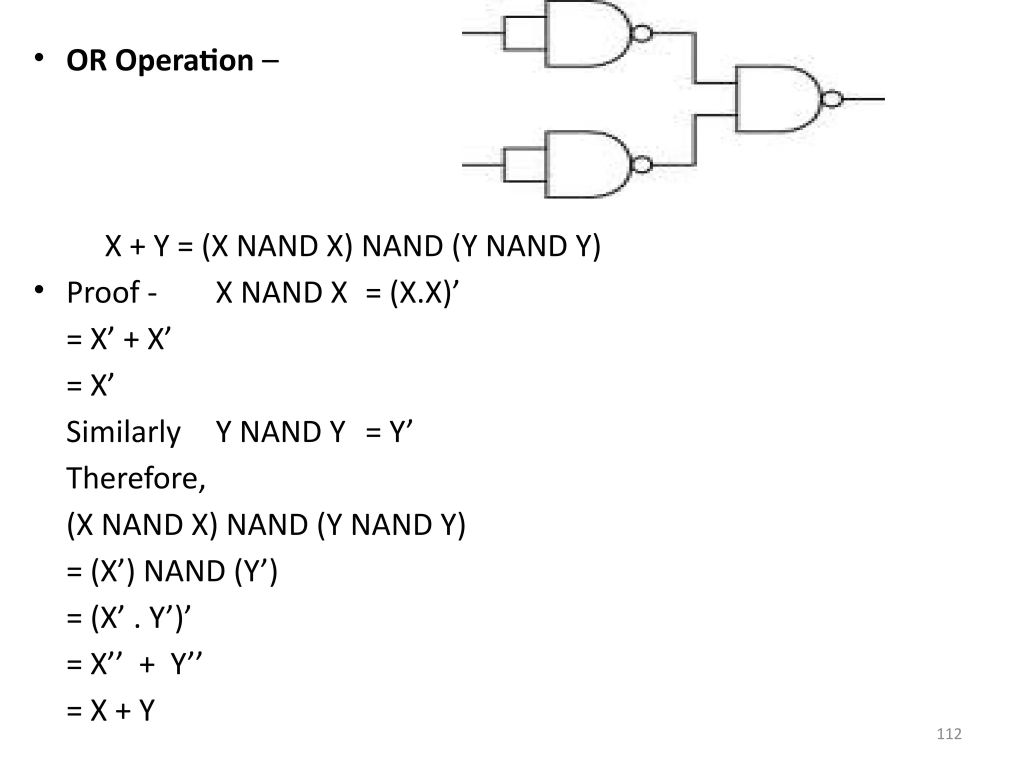
![111
• AND Operation –
X . Y = (X NAND Y) NAND (X NAND Y)
• Proof - X NAND Y = (X.Y)’
= X’ + Y’
(X NAND Y) NAND (X NAND Y)
= (X’ + Y’) NAND (X’ + Y’)
= [(X’ + Y’) . (X’ + Y’)]’
= (X’ + Y’)’ + (X’ + Y’)’
= (X’’ . Y’’) + (X’’ . Y’’)
= (X . Y) + (X . Y)
= X . Y](https://image.slidesharecdn.com/deupdated-240927103330-16694ebe/75/General-concepts-of-digital-electronics-and-111-2048.jpg)

![123
• Maps for Full Adder
SUM
S = x’y’z + x’yz’ + xy’z’ + xyz
CARRY
C = xy + xz + yz
YZ
X
[00] Y’Z’ [01] Y’Z [11]YZ [10]YZ’
[0] X’
1
1
[1] X 1 1
YZ
X
[00] Y’Z’ [01] Y’Z [11]YZ [10]YZ’
[0] X’ 1
[1] X 1 1 1](https://image.slidesharecdn.com/deupdated-240927103330-16694ebe/75/General-concepts-of-digital-electronics-and-123-2048.jpg)
![127
• Maps for Full Subtractor
Difference
D = x’y’z + x’yz’ + xy’z’ + xyz
Borrow
B = x’y + x’z + yz
YZ
X
[00] Y’Z’ [01] Y’Z [11]YZ [10]YZ’
[0] X’
1
1
[1] X 1 1
YZ
X
[00] Y’Z’ [01] Y’Z [11]YZ [10]YZ’
[0] X’ 1 1 1
[1] X 1](https://image.slidesharecdn.com/deupdated-240927103330-16694ebe/75/General-concepts-of-digital-electronics-and-127-2048.jpg)

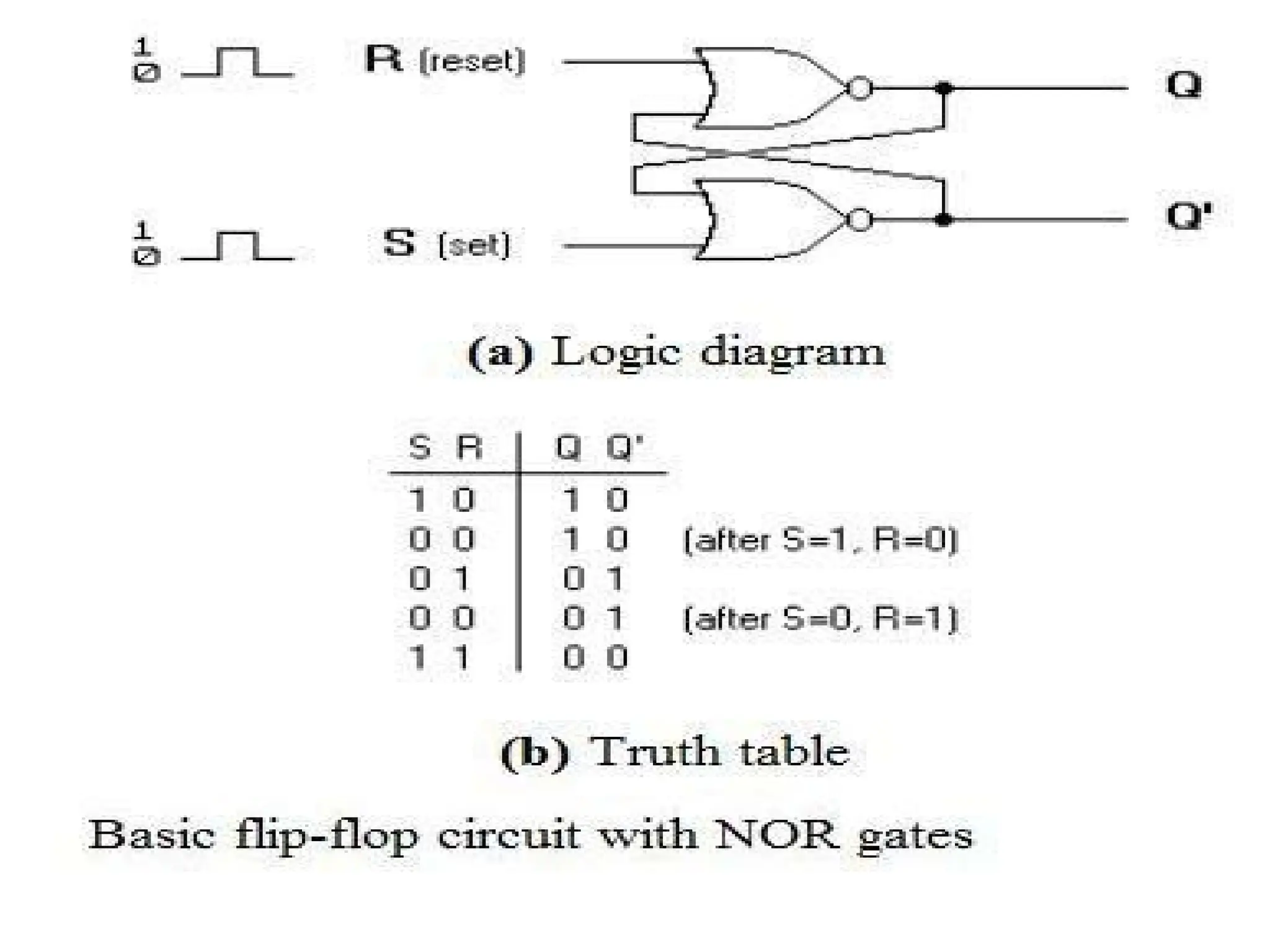
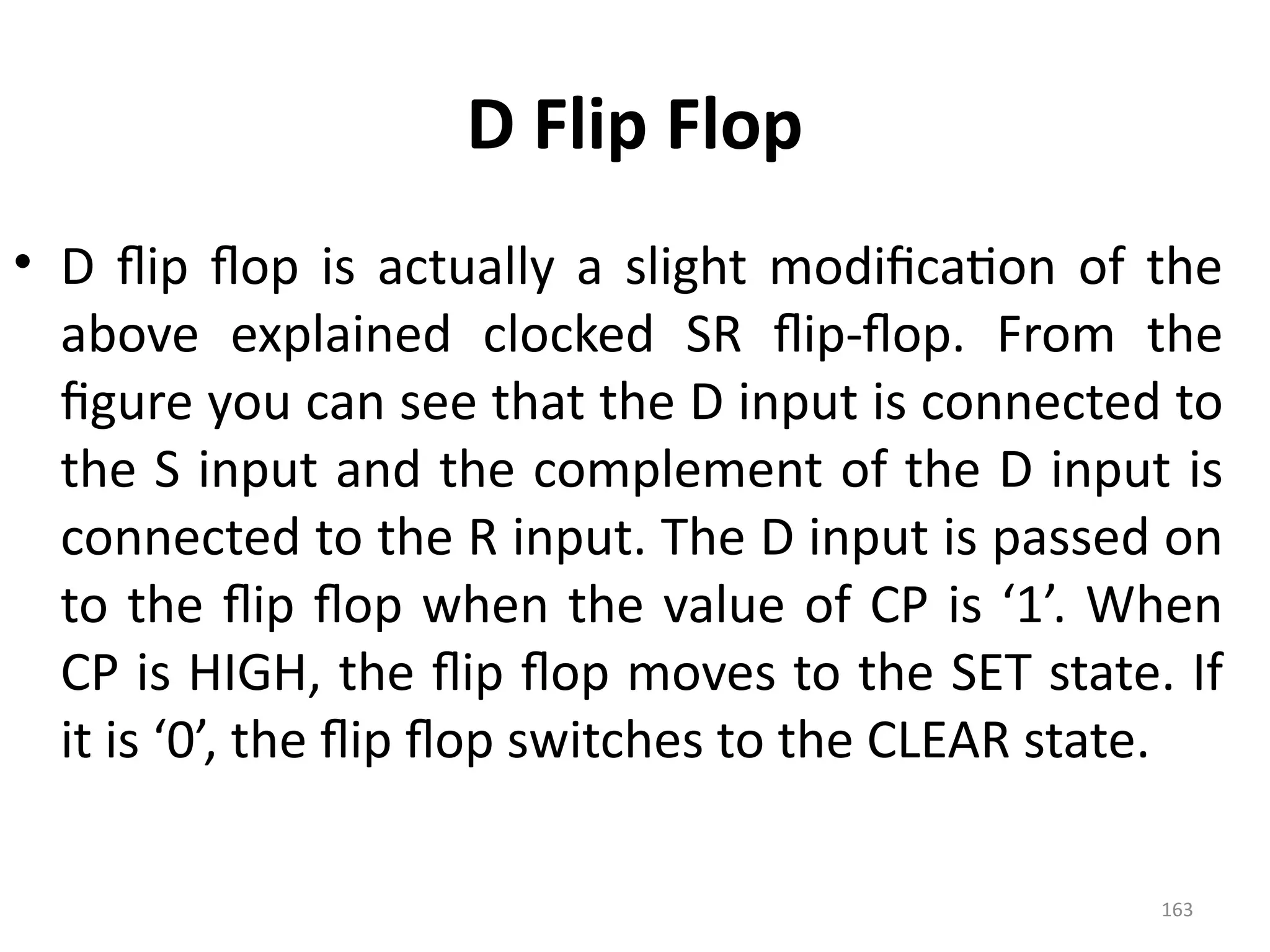
![156
• From the diagram it is evident that the flip flop has
mainly four states. They are
– S=1, R=0—Q=1, Q’=0
• This state is also called the SET state.
– S=0, R=1—Q=0, Q’=1
• This state is known as the RESET state.
– In both the states you can see that the outputs are just
compliments of each other and that the value of Q follows
the value of S.
– S=0, R=0—Q & Q’ = Remember
• If both the values of S and R are switched to 0, then the circuit
remembers the value of S and R in their previous state.
– S=1, R=1—Q=0, Q’=0 [Invalid]
• This is an invalid state because the values of both Q and Q’ are 0.
They are supposed to be compliments of each other. Normally, this
state must be avoided.](https://image.slidesharecdn.com/deupdated-240927103330-16694ebe/75/General-concepts-of-digital-electronics-and-156-2048.jpg)
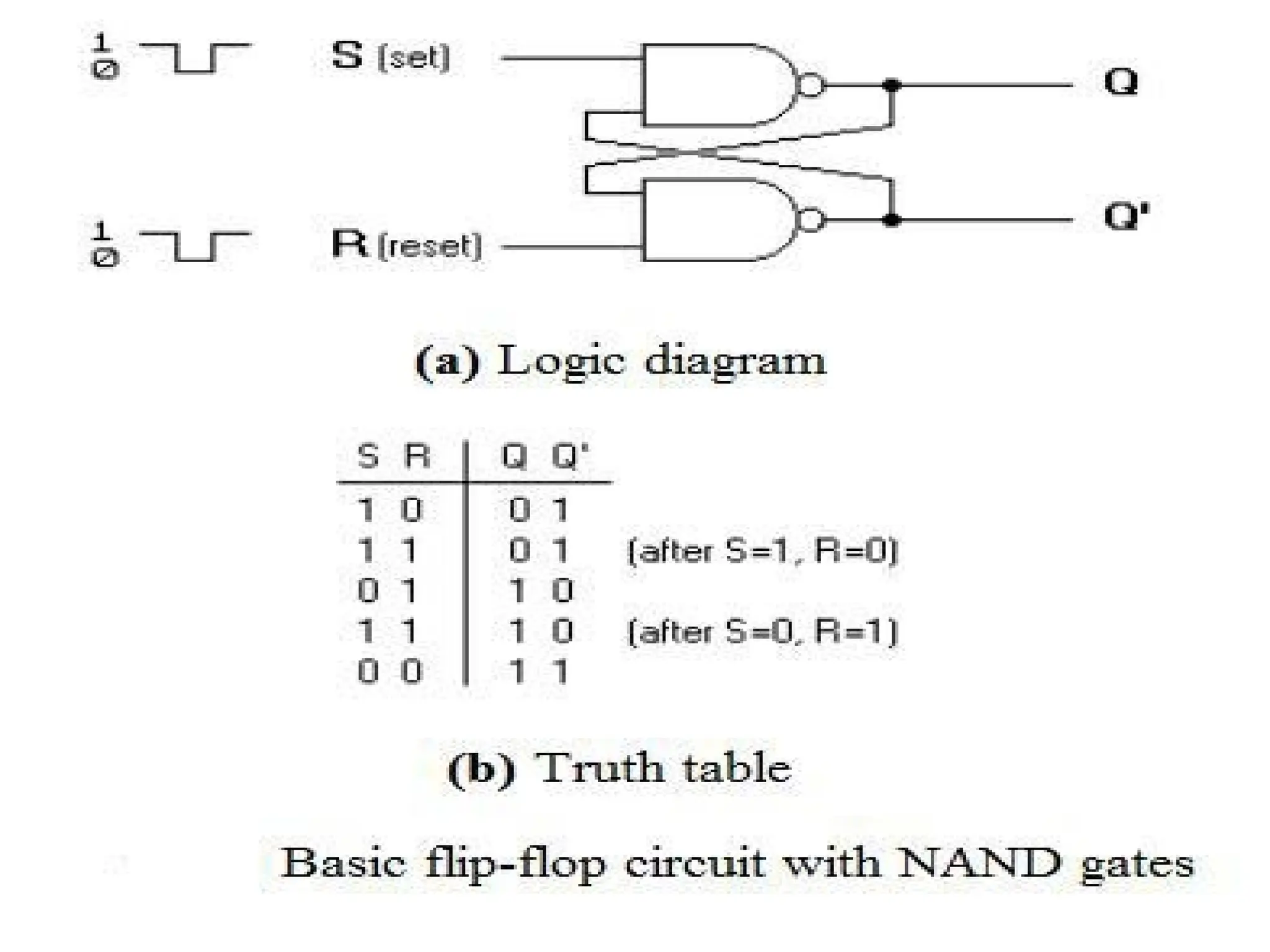
![158
• Like the NOR Gate S-R flip flop, this one also has four
states. They are
– S=1, R=0—Q=0, Q’=1
• This state is also called the SET state.
– S=0, R=1—Q=1, Q’=0
• This state is known as the RESET state.
– In both the states you can see that the outputs are just
compliments of each other and that the value of Q follows
the compliment value of S.
– S=0, R=0—Q=1, & Q’ =1 [Invalid]
• If both the values of S and R are switched to 0 it is an invalid state
because the values of both Q and Q’ are 1. They are supposed to be
compliments of each other. Normally, this state must be avoided.
– S=1, R=1—Q & Q’= Remember
• If both the values of S and R are switched to 1, then the circuit
remembers the value of S and R in their previous state.](https://image.slidesharecdn.com/deupdated-240927103330-16694ebe/75/General-concepts-of-digital-electronics-and-158-2048.jpg)
![165
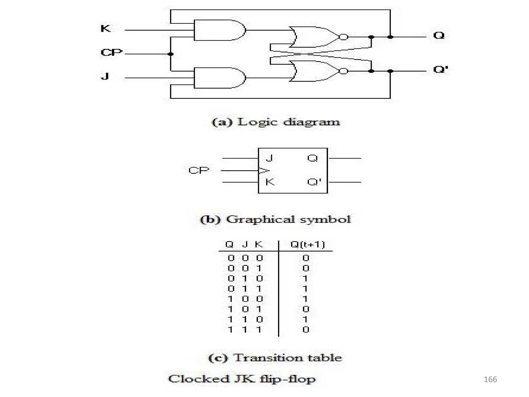
J-K Flip Flop
• A J-K flip flop can also be defined as a modification of the S-R flip flop. The only difference
is that the intermediate state is more refined and precise than that of a S-R flip flop.
• The behavior of inputs J and K is same as the S and R inputs of the S-R flip flop. The letter
J stands for SET and the letter K stands for CLEAR.
• When both the inputs J and K have a HIGH state, the flip-flop switch to the complement
state. So, for a value of Q = 1, it switches to Q=0 and for a value of Q = 0, it switches to
Q=1.
• The circuit includes two 3-input AND gates. The output Q of the flip flop is returned back
as a feedback to the input of the AND along with other inputs like K and clock pulse [CP].
So, if the value of CP is ‘1’, the flip flop gets a CLEAR signal and with the condition that
the value of Q was earlier 1. Similarly output Q’ of the flip flop is given as a feedback to
the input of the AND along with other inputs like J and clock pulse [CP]. So the output
becomes SET when the value of CP is 1 only if the value of Q’ was earlier 1.
• The output may be repeated in transitions once they have been complimented for J=K=1
because of the feedback connection in the JK flip-flop. This can be avoided by setting a
time duration lesser than the propagation delay through the flip-flop. The restriction on
the pulse width can be eliminated with a master-slave or edge-triggered construction.](https://image.slidesharecdn.com/deupdated-240927103330-16694ebe/75/General-concepts-of-digital-electronics-and-165-2048.jpg)
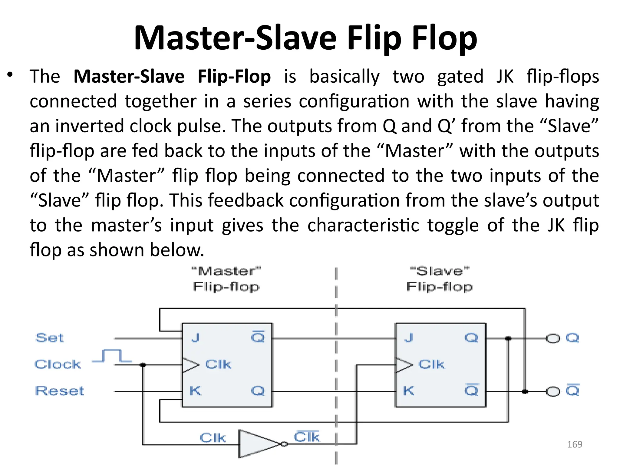
![171
• From the above figure we can see that both the
J-K flip flops are presented in a series
connection.
• The output of the master J-K flip flop is fed to
the input of the slave J-K flip flop.
• The output of the slave J-K flip flop is given as a
feedback to the input of the master J-K flip flop.
• The clock pulse [Clk] is given to the master J-K
flip flop and it is sent through a NOT Gate and
thus inverted before passing it to the slave J-K
flip flop.](https://image.slidesharecdn.com/deupdated-240927103330-16694ebe/75/General-concepts-of-digital-electronics-and-171-2048.jpg)