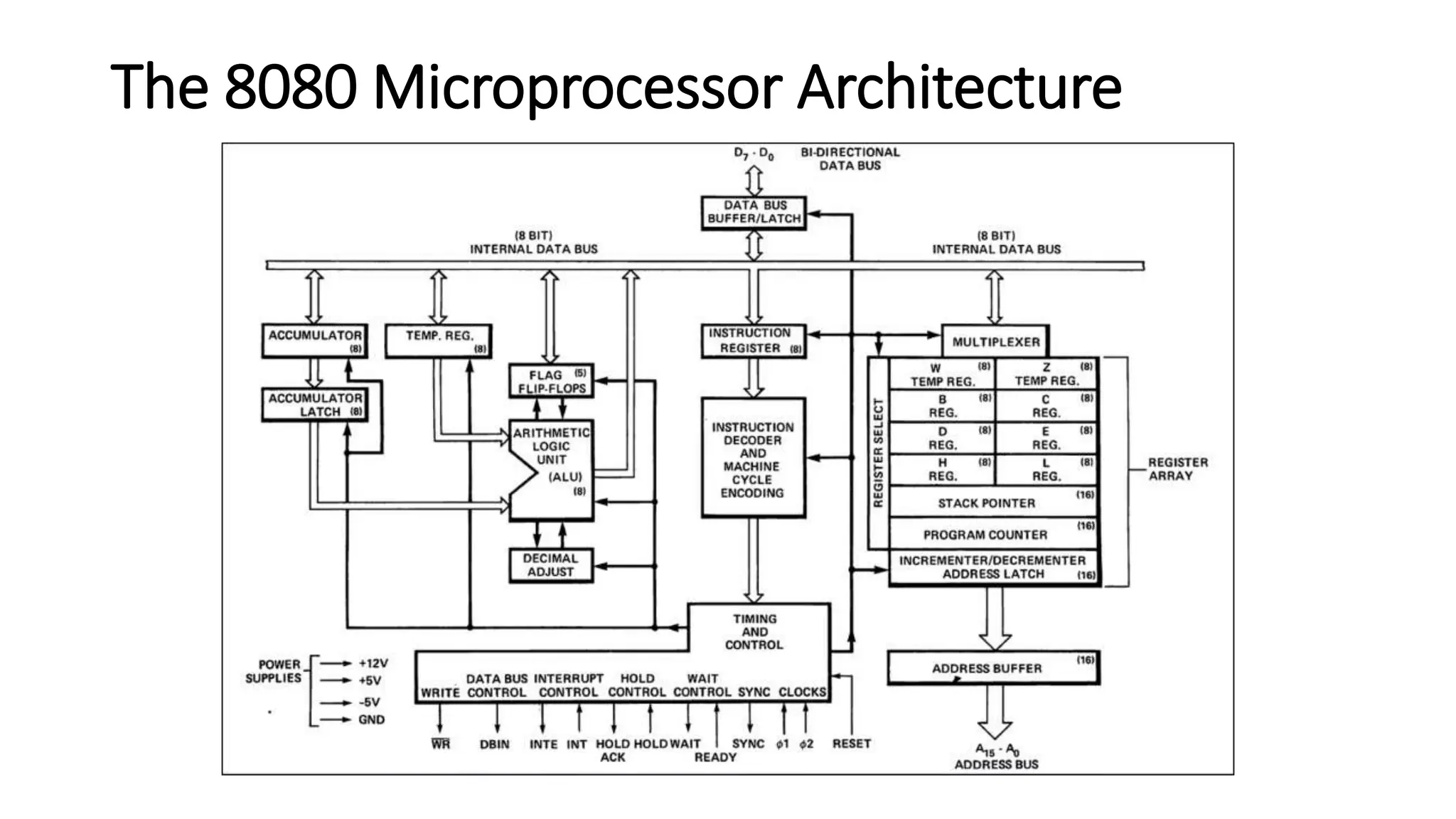
The 8080 Microprocessor
8080 Microprocessor
Architecture
The 8080 Microprocessor Architecture
Accumulator & Accumulator Latch
Accumulator
A register that stores one of the operands
to be manipulated by the ALU.
It can be both a source (operand) and a
destination (result) register.
Accumulator Latch
Holds the current value of the accumulator
register so as not be changed during
processing in the ALU.
Temporary Register
 The temporary register (TMP) receives
information from the internal bus and
can send all or portions of it to the ALU,
the flag register and the internal bus.
 The ALU is fed by the temporary register
(TMP).
Condition Flags
The Flag is an 8-bit register having five 1-bit flags.
A flag is set by forcing the bit to 1, and reset by
forcing the bit to 0.
The 5 Flags:
Zero Flag: If the result of an instruction has the
value ‘0’, this zero flag is set; or else, it is reset.
Sign Flag: If the MSB bit of an instruction has
the value ‘1’, this flag is set; or else, it is reset.
Parity Flag: If the number of the set bits in the
result has even value, this flag is set; or else, it is
reset.
Condition Flags
The 5 Flags (cont’d):
Carry Flag: If there was a carry during borrow,
addition, subtraction or comparison, this flag is
set; or else, it is reset.
Auxiliary Carry: If there was a carry out from 3-
bit to 4-bit of the result, this flag is set; otherwise,
it is reset.
Arithmetic Logic Unit (ALU)
The ALU contains: an 8-bit accumulator, an 8-bit
temporary accumulator (ACT), a 5-bit flag register:
zero, carry, sign, parity and auxiliary carry and an 8-
bit temporary register (TMP).
Arithmetic, logical and rotate operations are
performed in the ALU.
The ALU also feeds the flag register.
The temporary register (TMP) receives information
from the internal bus and can send all or portions of
it to the ALU, the flag register and the internal bus.
DAA (Decimal Adjust Accumulator)
The 8-bit number in the accumulator is adjusted to
form two four-bit Binary-Coded-Decimal digits by
the following process:
If the value of the least significant 4 bits of the
accumulator is greater than 9 or if the AC flag is
set, 6 is added to the accumulator.
If the value of the most significant 4 bits of the
accumulator is now greater than 9, or if the CY
flag is set, 6 is added to the most significant 4
bits of the accumulator.
NOTE: All flags are affected.
Timing and Control
Six timing (SYNC, DBIN, WAIT, WR,
HLDA and INTE)
• SYNC (output) - SYNCHRONIZING
SIGNAL; the SYNC pin provides a
signal to indicate the beginning of
each machine cycle.
• DBIN (output) - DATA BUS IN; the DBIN
signal indicates to external circuits that
the data bus is in the input mode. This
signal should be used to enable the gating
of data onto the 8080A data bus from
memory or I/O.
• WAIT (output) – WAIT; the WAIT signal
acknowledges that the CPU is in a WAIT
state.
• WR’ (output) – WRITE; the WR signal is
used for memory WRITE or I/O output
control. The data on the data bus is stable
while the WR signal is active low (WR’ = 0).
Timing and Control
• INTE (output) – INTERRUPT ENABLE;
indicates the content of the
internal interrupt enable flip/flop.
This flip/flop may be set or reset by
the Enable and Disable Interrupt
instructions and inhibits interrupts
from being accepted by the CPU
when it is reset. It is automatically
reset (disabling further interrupts)
at time T1 of the instruction fetch
cycle (M1) when an interrupt is
accepted and is also reset by the
RESET signal.
• HLDA (output) – HOLD ACKNOWLEDGE;
the HLDA signal appears in response to
the HOLD signal and indicates that the
data and address bus will go to the high
impedance state. The HLDA signal
begins at:
• T3 for READ memory or input.
• The Clock Period following T3 for WR
ITE memory or OUTPUT operation.
In either case, the HLDA signal
appears after the rising edge of CLK1
and high impedance occurs after the
rising edge of CLK2.
Timing and Control
Four control inputs (READY, HOLD, INT
and RESET)
• READY; the READY signal indicates to
the 8080A that valid memory or
input data is available on the 8080A
data bus.
• HOLD (input) – HOLD; this signal
requests the CPU to enter the HOLD
state. The HOLD state allows an
external device to gain control of the
8080A address and data bus.
• INT (input) – INTERRUPT REQUEST; the
CPU recognizes an interrupt request on
this line at the end of the current
instruction or while halted. If the CPU is
in the HOLD state or if the Interrupt
Enable flip/flop is reset it will not honor
the request.
• RESET (input) – RESET; while the RESET
signal is activated, the content of the
program counter is cleared. After
RESET, the program will start at location
0 in memory.
Instruction Register and Control
• During an instruction fetch, the first byte of an
instruction (containing the OP code) is
transferred from the internal bus to the 8-bit
instruction register.
• The contents of the instruction register are, in
turn, available to the instruction decoder. The
output of the decoder, combined with various
timing signals, provides the control signals for
the register array, ALU and data buffer blocks. In
addition, the outputs from the instruction
decoder and external control signals feed the
timing and state control section which generates
the state and cycle timing signals.
Address Buffer
• A Buffer is another Logic Gate that
has only one Input, its Output
follows the same Logic State as
the Input. The Buffer is used as
delay element in Digital
Electronics. It is also a Current-
Boost-Up element, which is used
to increase the capability of the
Output of one gate to drive a
number of other gates.
Summary of the 8080 Microprocessor
Architecture
8080 Microprocessor Functional Units:
Register array and address logic
Arithmetic and logic unit (ALU)
Instruction register and control section
Bi-directional, 3-state data bus buffer
Registers:
Program counter 16-bit (PC)
Stack pointer 16-bit (SP)
General Purpose Registers (6 x 8-bit general purpose
registers arranged in pairs (B & C; D & E; and H & L
Summary of the 8080 Microprocessor
Architecture
Registers (cont’d):
Temporary register pair (W & Z)
Seven 8-bit registers (A-E, H, L)
Bus & I/Os
External bi-directional data bus (8-bit)
Internal bi-directional data bus (8-bit)
Address bus (16-bit)
8080 Microprocessor
Pinout
The 8080 Microprocessor Pinout
• Address bus (A0-A15) (output)
• Data bus (D0-D7) (input/output)
• SYNC (output)
• DBIN (output)
• READY (input)
• WAIT (output)
• WR’ (output)
• HOLD (input)
• HLDA (output)
• INTE (output)
• INT (input)
The 8080 Microprocessor Pinout
• RESET (input)
• Vss – Ground Reference.
• Vdd – +12V +/-5%
• Vcc – +5V +/-5%
• Vbb – -5V +/-5%
• CLK1 & CLK2 – 2 externally supplied clock
phases (non TTL compatible).
Block Diagram of 8080 Based Computer
8080 Microprocessor
Instruction Set
The 8080 Instruction Set
• Data Transfer Group
MOV <r1,r2> - Move register, <r,M> - Move from
memory, <M,r> - Move to memory
MVI <r,data> - Move immdediate, <M,data> - Move to
memory immediate
LXI <rp,data 16> - Load register pair immediate
LDA <addr> - Load accumulator direct
STA <addr> - Store accumulator direct
LHLD <addr> - Load H and L direct
The 8080 Instruction Set
• Data Transfer Group (cont’d)
SHLD <addr> - Store H and L direct
LDAX <rp> - Load accumulator indirect
STAX <rp> - Store accumulator indirect
XCHG - Exchange H and L with D and E
The 8080 Instruction Set
• Arithmetic Group
ADD <r> - Add register, <M> - Add memory
ADI <data> - Add immediate
ADC <r> - Add register with carry, <M> - Add memory
with carry
ACI <data> - Add immediate with carry
SUB <r> - Subtract register, <M> - Subtract memory
SUI <data> - Subtract immediate
SBB <r> - Subtract register with borrow, <M> - Subtract
memory with borrow
The 8080 Instruction Set
• Arithmetic Group (cont’d)
SBI <data> - Subtract immediate with borrow
INR <r> - Increment register, <M> - Increment memory
DCR <r> - Decrement register, <M> - Decrement memory
INX <rp> - Increment register pair
DCX <rp> - Decrement register pair
DAD <rp> - Add register pair to H and L
DAA - Decimal adjust accumulator
The 8080 Instruction Set
• Logical Group
ANA <r> - AND register, <M> - AND memory
ANI <data> - AND immediate
XRA <r> - Exclusive OR register, <m> - Exclusive OR
memory
XRI <data> - Exclusive OR immediate
ORA <r> - OR register, <M> - OR memory
ORI <data> - OR immediate
CMP <r> - Compare register, <M> - Compare memory
The 8080 Instruction Set
• Logical Group (cont’d)
CPI <data> - Compare immediate
RLC - Rotate left
RRC - Rotate right
RAL - Rotate left through carry
RAR - Rotate right through carry
CMA - Complement accumulator
CMC - Complement carry
STC - Set carry
The 8080 Instruction Set
• Branch Group
JMP <addr> - Jump to address
JCONDITION <addr> - Conditional jump to address (ex. IF)
CALL <addr> - Call address
CCONDITION <addr> - Condition call address (ex. IF)
RET - Return
RCONDITION - Conditional return
RST <n> - Restart
PCHL - Jump H and L indirect - move H and L to PC
The 8080 Instruction Set
• Stack, I/O and Machine Control Group
PUSH <rp> - Push register pair indirect
PUSH PSW - Push processor status word
POP <rp> - Pop (move) to register pair indirect
POP PSW - Pop processor status word
XTHL - Exchange stack top with H and L
SPHL - Move HL to SP
IN <port> - Input data from port
OUT <port> - Output data to port
The 8080 Instruction Set
• Stack, I/O and Machine Control Group (cont’d)
EI - Enable interrupts
DI - Disable interrupts
HLT - Halt or stop the processor
NOP - No operation
8080 Microprocessor
Instruction Set
Summary
8080 Microprocessor
Fetching and Executing
Instructions
General CPU Architecture
Instruction 1: Fetch – Program Add
0
Instruction 1: Fetch – Complete!
1
Instruction 1: Execute – Complete!
2
Instruction 2: Fetch
2
Instruction 2: Fetch – Complete!
3
Instruction 2: Execute – Complete!
4
Instruction 3: Fetch
4
Instruction 3: Fetch – Complete!
5
Instruction 3: Execute – Complete!
6
Instruction 4: Fetch
6
Instruction 4: Fetch – Complete!
7
Instruction 4: Execute – Complete!
8
Instruction 5: Fetch – Complete!
8
8080 Microprocessor
Timing Diagrams
Basic 8080 Instruction Cycle
Input Instruction Cycle
Output Instruction Cycle
Interrupt Timing
Hold Operation (Read Mode)
Hold Operation (Write Mode)
Halt Timing
Reset
HOLD and INT in HALT State
8080 Microprocessor
Timing Summary
8080 Microprocessor
Programming
Addition of Two 16-Bit Numbers with Carry
Subtraction of Two 8-Bit Numbers with Borrow
END OF PRESENTATION
References:
• Intel 8080 Microcomputer Systems User's Manual September 1975 by Intel Corporation
• https://slideplayer.com/slide/14999644/
• Microprocessor Interfacing Lab Manual

Discussion on 8080 Microprocessor_r1 - Everyting you need to know.pptx

  • 1.
  • 2.
  • 3.
  • 4.
    Accumulator & AccumulatorLatch Accumulator A register that stores one of the operands to be manipulated by the ALU. It can be both a source (operand) and a destination (result) register. Accumulator Latch Holds the current value of the accumulator register so as not be changed during processing in the ALU.
  • 5.
    Temporary Register  Thetemporary register (TMP) receives information from the internal bus and can send all or portions of it to the ALU, the flag register and the internal bus.  The ALU is fed by the temporary register (TMP).
  • 6.
    Condition Flags The Flagis an 8-bit register having five 1-bit flags. A flag is set by forcing the bit to 1, and reset by forcing the bit to 0. The 5 Flags: Zero Flag: If the result of an instruction has the value ‘0’, this zero flag is set; or else, it is reset. Sign Flag: If the MSB bit of an instruction has the value ‘1’, this flag is set; or else, it is reset. Parity Flag: If the number of the set bits in the result has even value, this flag is set; or else, it is reset.
  • 7.
    Condition Flags The 5Flags (cont’d): Carry Flag: If there was a carry during borrow, addition, subtraction or comparison, this flag is set; or else, it is reset. Auxiliary Carry: If there was a carry out from 3- bit to 4-bit of the result, this flag is set; otherwise, it is reset.
  • 8.
    Arithmetic Logic Unit(ALU) The ALU contains: an 8-bit accumulator, an 8-bit temporary accumulator (ACT), a 5-bit flag register: zero, carry, sign, parity and auxiliary carry and an 8- bit temporary register (TMP). Arithmetic, logical and rotate operations are performed in the ALU. The ALU also feeds the flag register. The temporary register (TMP) receives information from the internal bus and can send all or portions of it to the ALU, the flag register and the internal bus.
  • 9.
    DAA (Decimal AdjustAccumulator) The 8-bit number in the accumulator is adjusted to form two four-bit Binary-Coded-Decimal digits by the following process: If the value of the least significant 4 bits of the accumulator is greater than 9 or if the AC flag is set, 6 is added to the accumulator. If the value of the most significant 4 bits of the accumulator is now greater than 9, or if the CY flag is set, 6 is added to the most significant 4 bits of the accumulator. NOTE: All flags are affected.
  • 10.
    Timing and Control Sixtiming (SYNC, DBIN, WAIT, WR, HLDA and INTE) • SYNC (output) - SYNCHRONIZING SIGNAL; the SYNC pin provides a signal to indicate the beginning of each machine cycle. • DBIN (output) - DATA BUS IN; the DBIN signal indicates to external circuits that the data bus is in the input mode. This signal should be used to enable the gating of data onto the 8080A data bus from memory or I/O. • WAIT (output) – WAIT; the WAIT signal acknowledges that the CPU is in a WAIT state. • WR’ (output) – WRITE; the WR signal is used for memory WRITE or I/O output control. The data on the data bus is stable while the WR signal is active low (WR’ = 0).
  • 11.
    Timing and Control •INTE (output) – INTERRUPT ENABLE; indicates the content of the internal interrupt enable flip/flop. This flip/flop may be set or reset by the Enable and Disable Interrupt instructions and inhibits interrupts from being accepted by the CPU when it is reset. It is automatically reset (disabling further interrupts) at time T1 of the instruction fetch cycle (M1) when an interrupt is accepted and is also reset by the RESET signal. • HLDA (output) – HOLD ACKNOWLEDGE; the HLDA signal appears in response to the HOLD signal and indicates that the data and address bus will go to the high impedance state. The HLDA signal begins at: • T3 for READ memory or input. • The Clock Period following T3 for WR ITE memory or OUTPUT operation. In either case, the HLDA signal appears after the rising edge of CLK1 and high impedance occurs after the rising edge of CLK2.
  • 12.
    Timing and Control Fourcontrol inputs (READY, HOLD, INT and RESET) • READY; the READY signal indicates to the 8080A that valid memory or input data is available on the 8080A data bus. • HOLD (input) – HOLD; this signal requests the CPU to enter the HOLD state. The HOLD state allows an external device to gain control of the 8080A address and data bus. • INT (input) – INTERRUPT REQUEST; the CPU recognizes an interrupt request on this line at the end of the current instruction or while halted. If the CPU is in the HOLD state or if the Interrupt Enable flip/flop is reset it will not honor the request. • RESET (input) – RESET; while the RESET signal is activated, the content of the program counter is cleared. After RESET, the program will start at location 0 in memory.
  • 13.
    Instruction Register andControl • During an instruction fetch, the first byte of an instruction (containing the OP code) is transferred from the internal bus to the 8-bit instruction register. • The contents of the instruction register are, in turn, available to the instruction decoder. The output of the decoder, combined with various timing signals, provides the control signals for the register array, ALU and data buffer blocks. In addition, the outputs from the instruction decoder and external control signals feed the timing and state control section which generates the state and cycle timing signals.
  • 14.
    Address Buffer • ABuffer is another Logic Gate that has only one Input, its Output follows the same Logic State as the Input. The Buffer is used as delay element in Digital Electronics. It is also a Current- Boost-Up element, which is used to increase the capability of the Output of one gate to drive a number of other gates.
  • 15.
    Summary of the8080 Microprocessor Architecture 8080 Microprocessor Functional Units: Register array and address logic Arithmetic and logic unit (ALU) Instruction register and control section Bi-directional, 3-state data bus buffer Registers: Program counter 16-bit (PC) Stack pointer 16-bit (SP) General Purpose Registers (6 x 8-bit general purpose registers arranged in pairs (B & C; D & E; and H & L
  • 16.
    Summary of the8080 Microprocessor Architecture Registers (cont’d): Temporary register pair (W & Z) Seven 8-bit registers (A-E, H, L) Bus & I/Os External bi-directional data bus (8-bit) Internal bi-directional data bus (8-bit) Address bus (16-bit)
  • 17.
  • 18.
    The 8080 MicroprocessorPinout • Address bus (A0-A15) (output) • Data bus (D0-D7) (input/output) • SYNC (output) • DBIN (output) • READY (input) • WAIT (output) • WR’ (output) • HOLD (input) • HLDA (output) • INTE (output) • INT (input)
  • 19.
    The 8080 MicroprocessorPinout • RESET (input) • Vss – Ground Reference. • Vdd – +12V +/-5% • Vcc – +5V +/-5% • Vbb – -5V +/-5% • CLK1 & CLK2 – 2 externally supplied clock phases (non TTL compatible).
  • 20.
    Block Diagram of8080 Based Computer
  • 22.
  • 23.
  • 24.
  • 25.
  • 26.
    The 8080 InstructionSet • Data Transfer Group MOV <r1,r2> - Move register, <r,M> - Move from memory, <M,r> - Move to memory MVI <r,data> - Move immdediate, <M,data> - Move to memory immediate LXI <rp,data 16> - Load register pair immediate LDA <addr> - Load accumulator direct STA <addr> - Store accumulator direct LHLD <addr> - Load H and L direct
  • 27.
    The 8080 InstructionSet • Data Transfer Group (cont’d) SHLD <addr> - Store H and L direct LDAX <rp> - Load accumulator indirect STAX <rp> - Store accumulator indirect XCHG - Exchange H and L with D and E
  • 28.
    The 8080 InstructionSet • Arithmetic Group ADD <r> - Add register, <M> - Add memory ADI <data> - Add immediate ADC <r> - Add register with carry, <M> - Add memory with carry ACI <data> - Add immediate with carry SUB <r> - Subtract register, <M> - Subtract memory SUI <data> - Subtract immediate SBB <r> - Subtract register with borrow, <M> - Subtract memory with borrow
  • 29.
    The 8080 InstructionSet • Arithmetic Group (cont’d) SBI <data> - Subtract immediate with borrow INR <r> - Increment register, <M> - Increment memory DCR <r> - Decrement register, <M> - Decrement memory INX <rp> - Increment register pair DCX <rp> - Decrement register pair DAD <rp> - Add register pair to H and L DAA - Decimal adjust accumulator
  • 30.
    The 8080 InstructionSet • Logical Group ANA <r> - AND register, <M> - AND memory ANI <data> - AND immediate XRA <r> - Exclusive OR register, <m> - Exclusive OR memory XRI <data> - Exclusive OR immediate ORA <r> - OR register, <M> - OR memory ORI <data> - OR immediate CMP <r> - Compare register, <M> - Compare memory
  • 31.
    The 8080 InstructionSet • Logical Group (cont’d) CPI <data> - Compare immediate RLC - Rotate left RRC - Rotate right RAL - Rotate left through carry RAR - Rotate right through carry CMA - Complement accumulator CMC - Complement carry STC - Set carry
  • 32.
    The 8080 InstructionSet • Branch Group JMP <addr> - Jump to address JCONDITION <addr> - Conditional jump to address (ex. IF) CALL <addr> - Call address CCONDITION <addr> - Condition call address (ex. IF) RET - Return RCONDITION - Conditional return RST <n> - Restart PCHL - Jump H and L indirect - move H and L to PC
  • 33.
    The 8080 InstructionSet • Stack, I/O and Machine Control Group PUSH <rp> - Push register pair indirect PUSH PSW - Push processor status word POP <rp> - Pop (move) to register pair indirect POP PSW - Pop processor status word XTHL - Exchange stack top with H and L SPHL - Move HL to SP IN <port> - Input data from port OUT <port> - Output data to port
  • 34.
    The 8080 InstructionSet • Stack, I/O and Machine Control Group (cont’d) EI - Enable interrupts DI - Disable interrupts HLT - Halt or stop the processor NOP - No operation
  • 35.
  • 39.
    8080 Microprocessor Fetching andExecuting Instructions
  • 41.
  • 42.
  • 43.
    Instruction 1: Fetch– Program Add 0
  • 44.
    Instruction 1: Fetch– Complete! 1
  • 45.
    Instruction 1: Execute– Complete! 2
  • 46.
  • 47.
    Instruction 2: Fetch– Complete! 3
  • 48.
    Instruction 2: Execute– Complete! 4
  • 49.
  • 50.
    Instruction 3: Fetch– Complete! 5
  • 51.
    Instruction 3: Execute– Complete! 6
  • 52.
  • 53.
    Instruction 4: Fetch– Complete! 7
  • 54.
    Instruction 4: Execute– Complete! 8
  • 55.
    Instruction 5: Fetch– Complete! 8
  • 56.
  • 58.
  • 60.
  • 62.
  • 64.
  • 66.
  • 68.
  • 70.
  • 72.
  • 74.
    HOLD and INTin HALT State
  • 76.
  • 89.
  • 90.
    Addition of Two16-Bit Numbers with Carry
  • 91.
    Addition of Two16-Bit Numbers with Carry
  • 92.
    Subtraction of Two8-Bit Numbers with Borrow
  • 93.
    Subtraction of Two8-Bit Numbers with Borrow
  • 94.
    END OF PRESENTATION References: •Intel 8080 Microcomputer Systems User's Manual September 1975 by Intel Corporation • https://slideplayer.com/slide/14999644/ • Microprocessor Interfacing Lab Manual

Editor's Notes

  • #42 MBR = Memory Buffer Register or Memory Data Register (MDR) – used by memory & I/O devices MAR = Memory Address Register – used to address memory to gain access of its content or in preparation for writing data into it.
  • #43 MBR = Memory Buffer Register or Memory Data Register (MDR) – used by memory & I/O devices MAR = Memory Address Register – used to address memory to gain access of its content or in preparation for writing data into it.