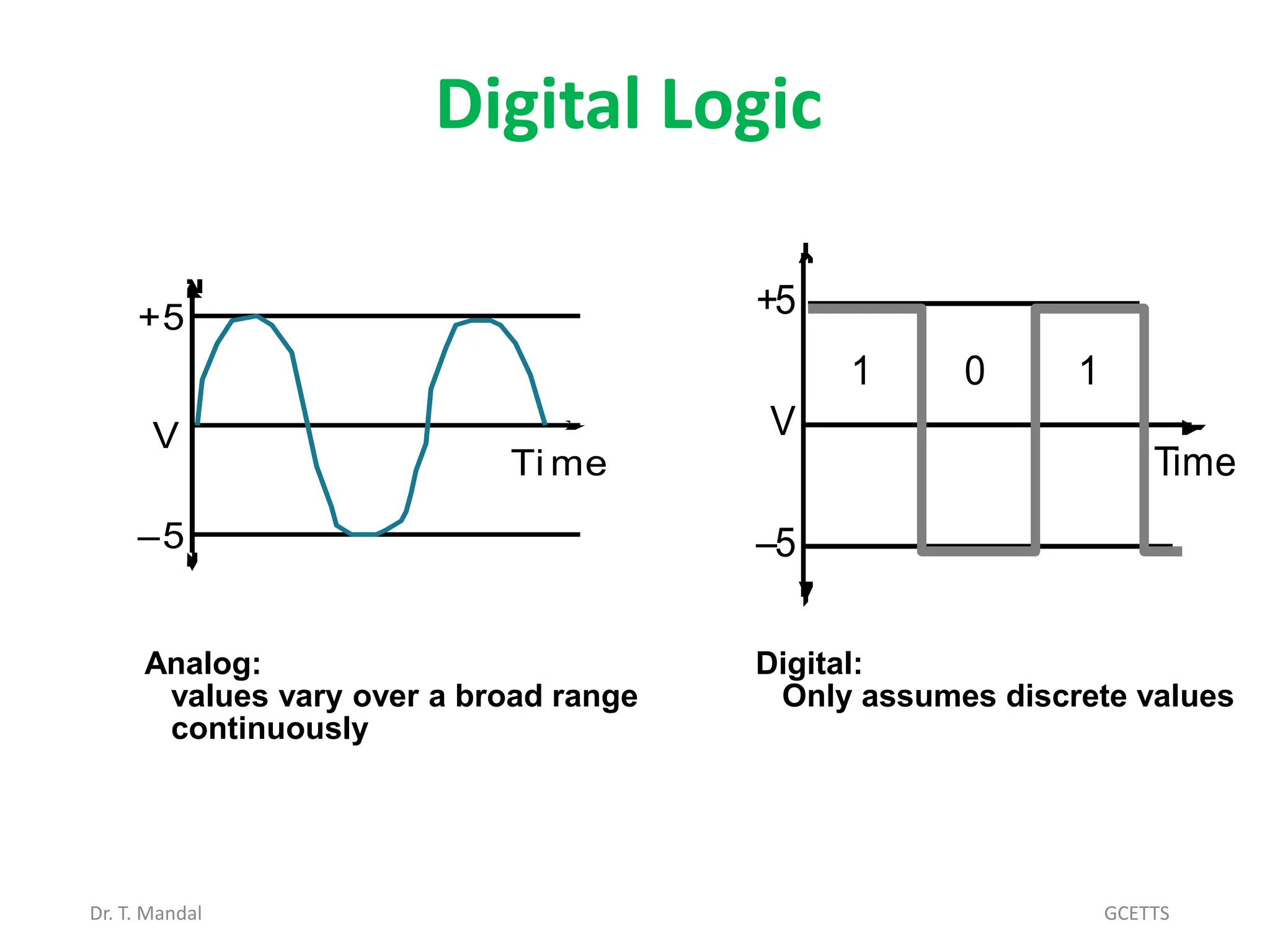
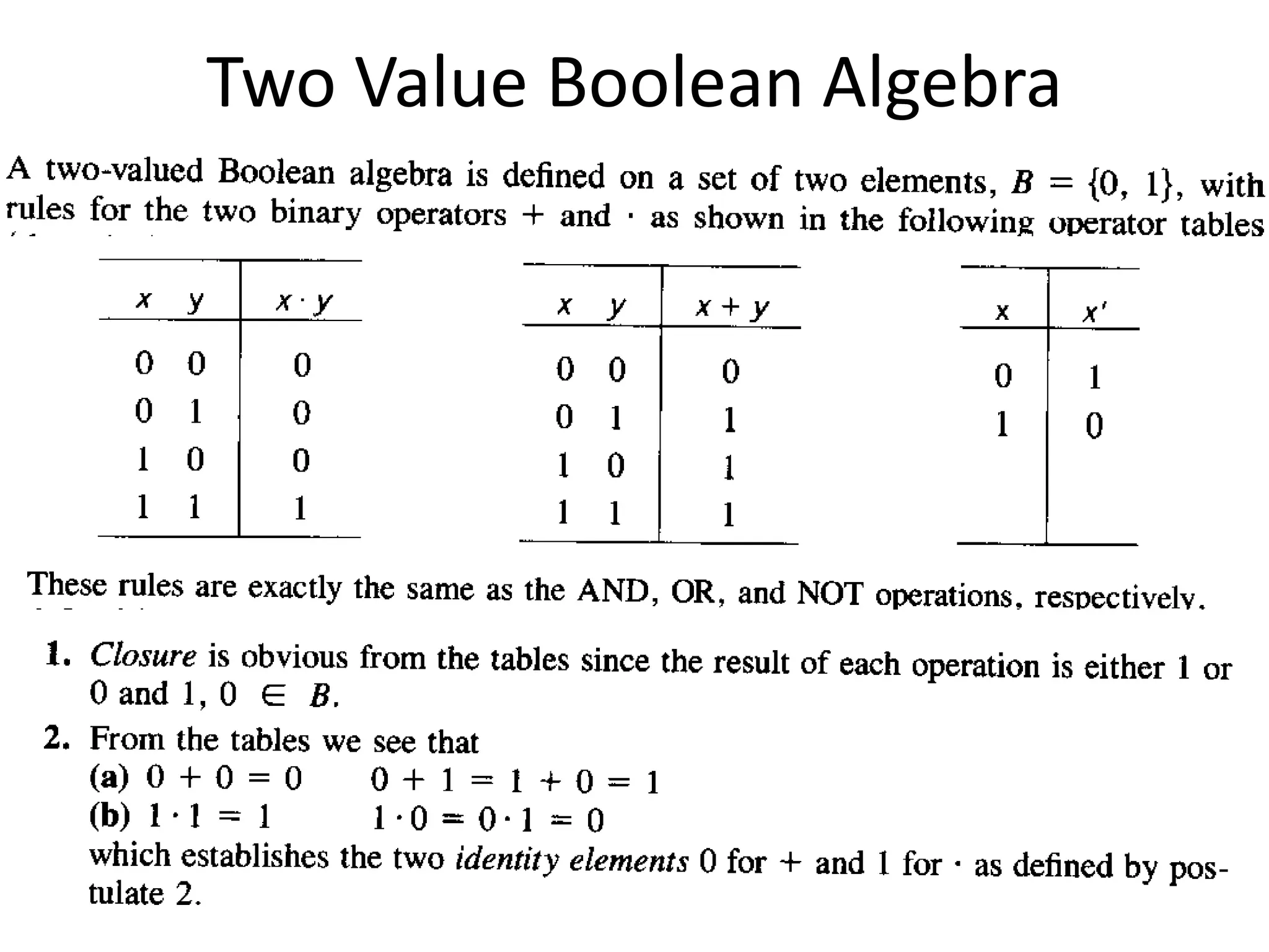
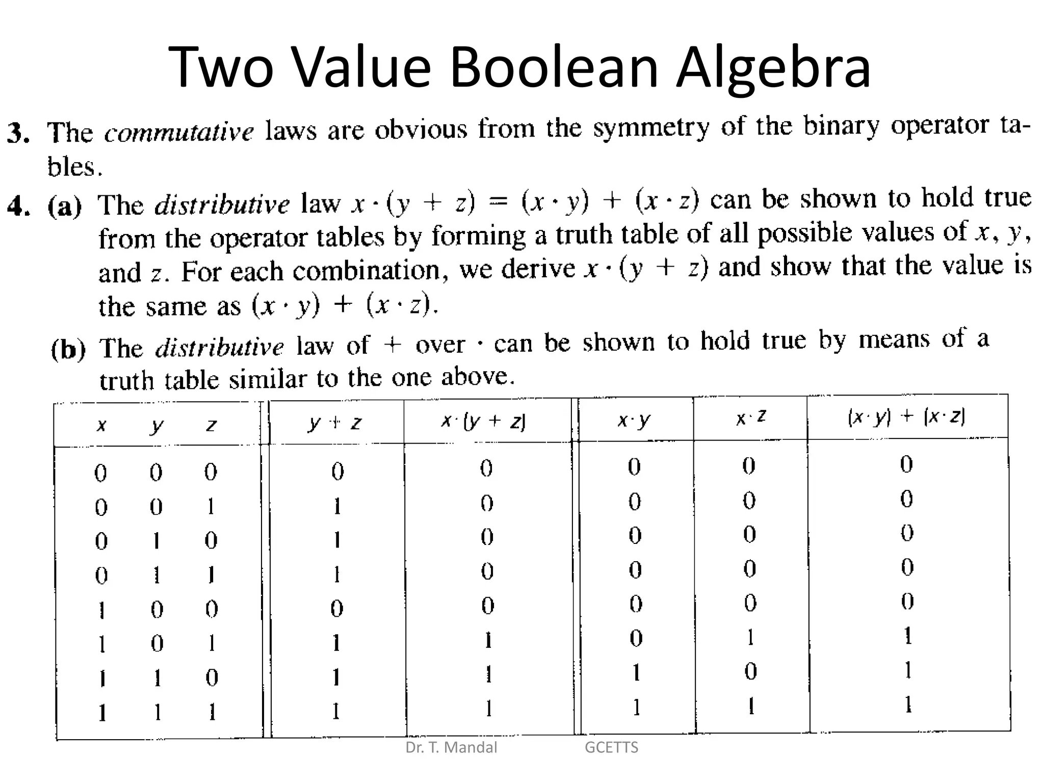
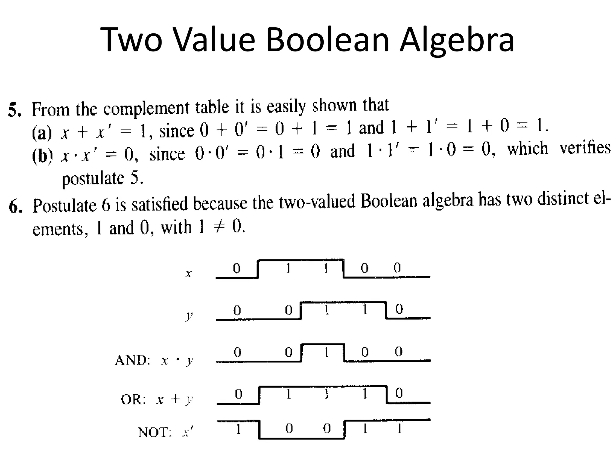
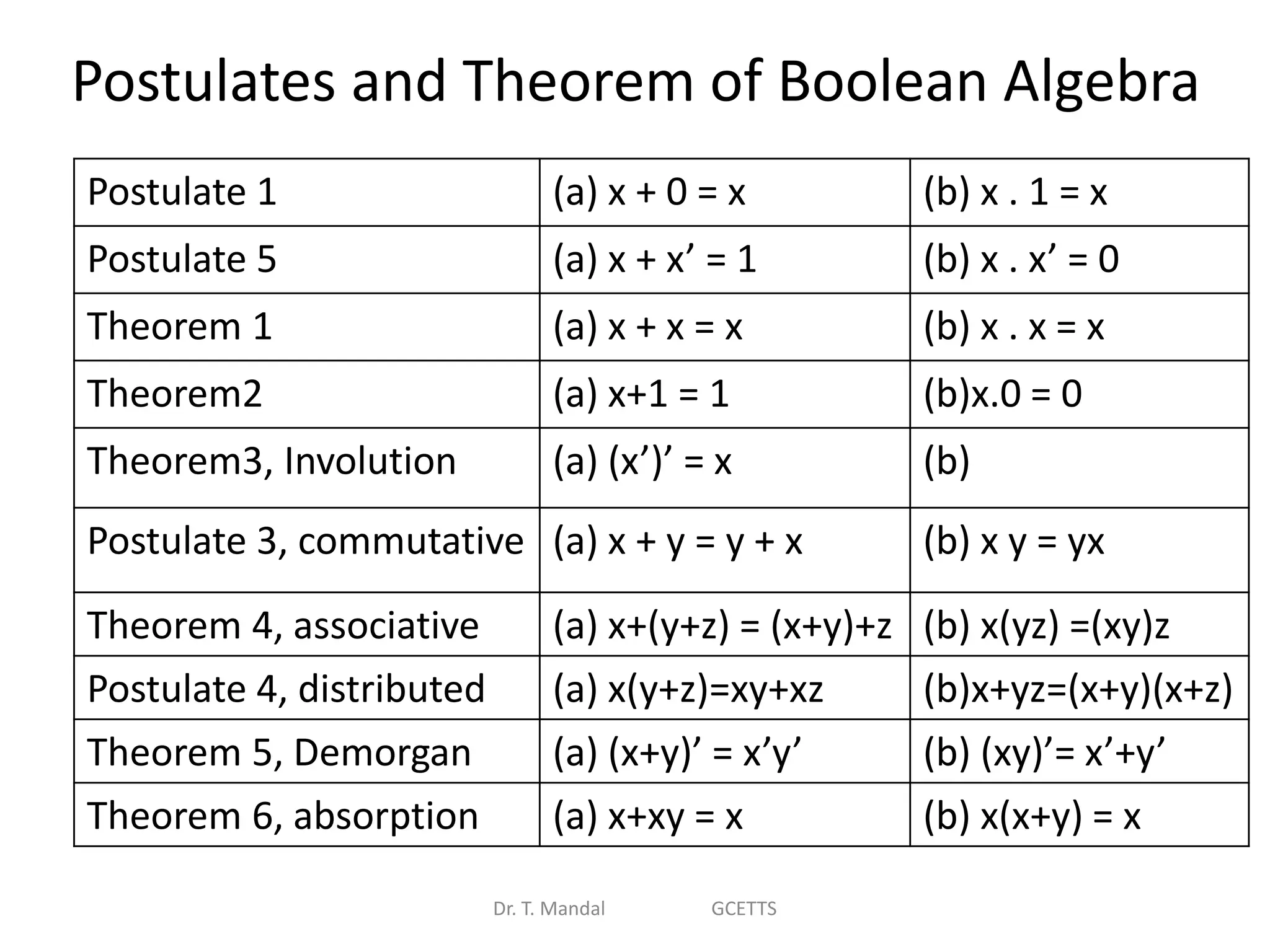
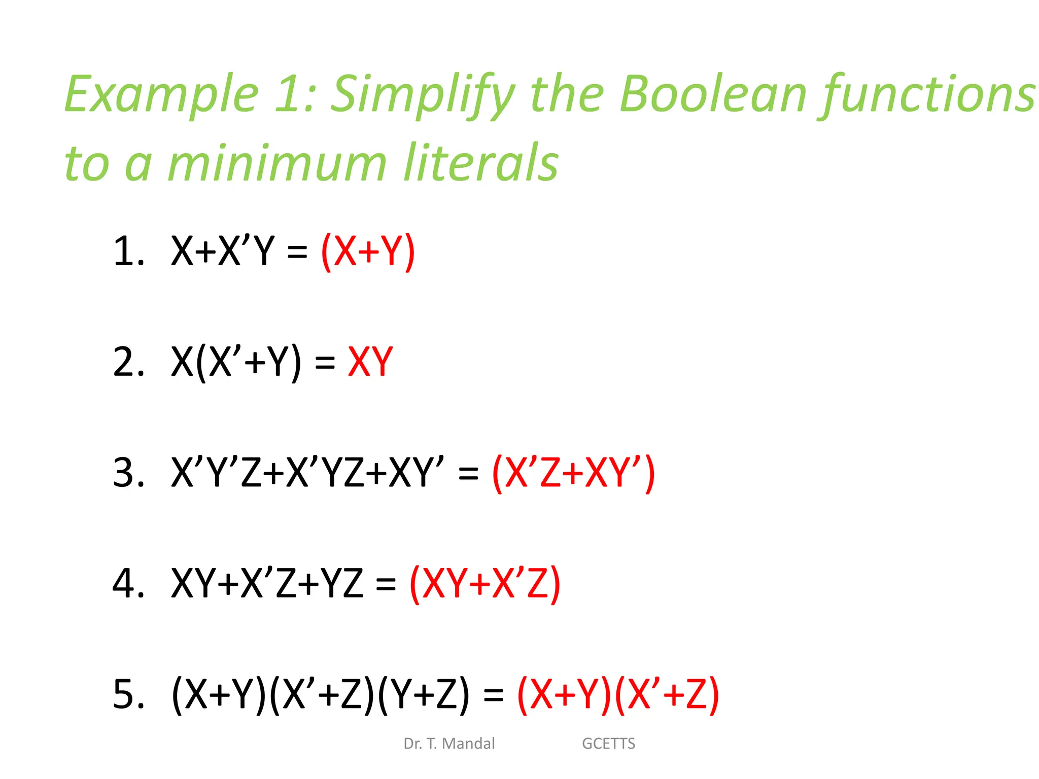
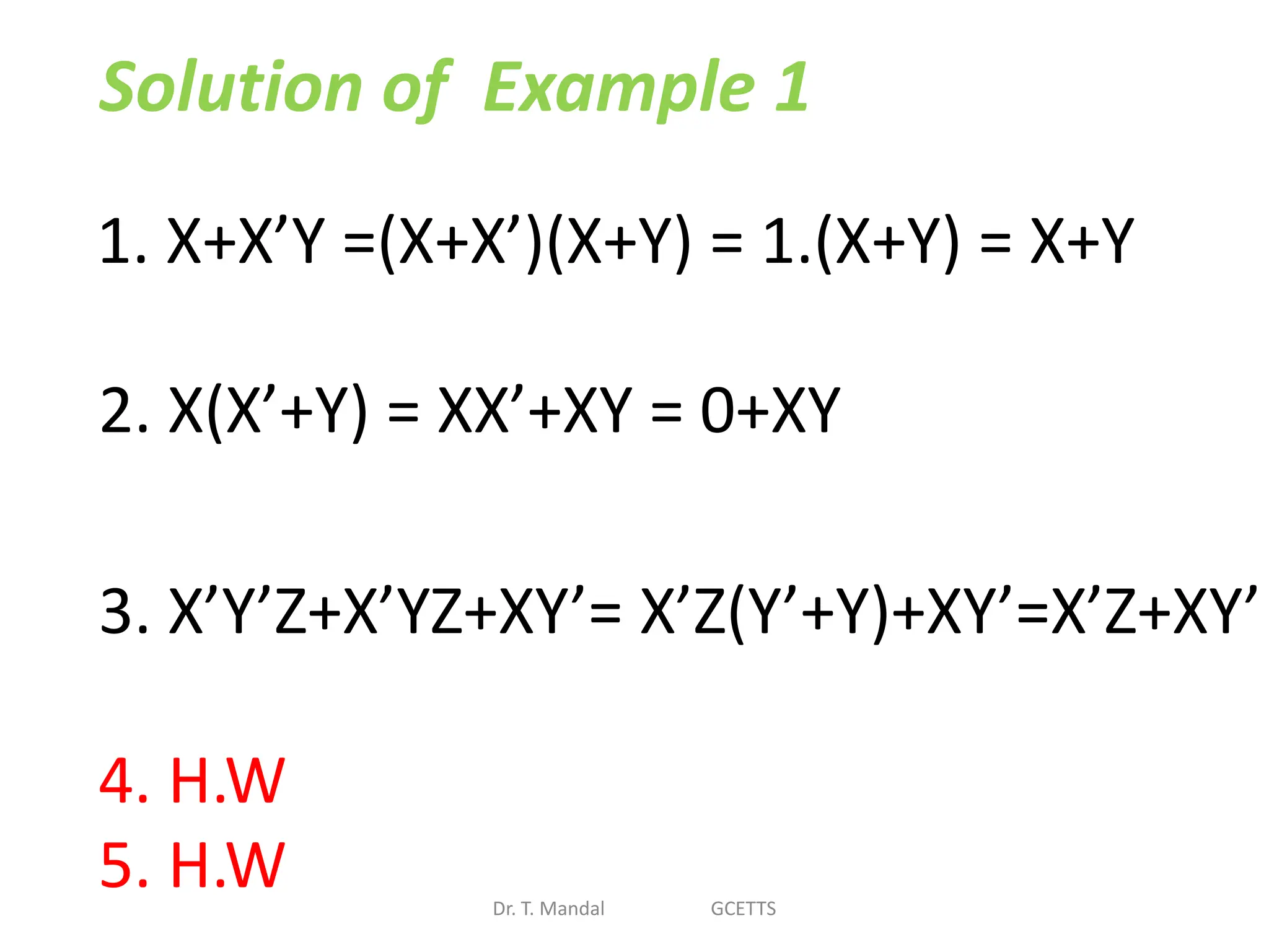
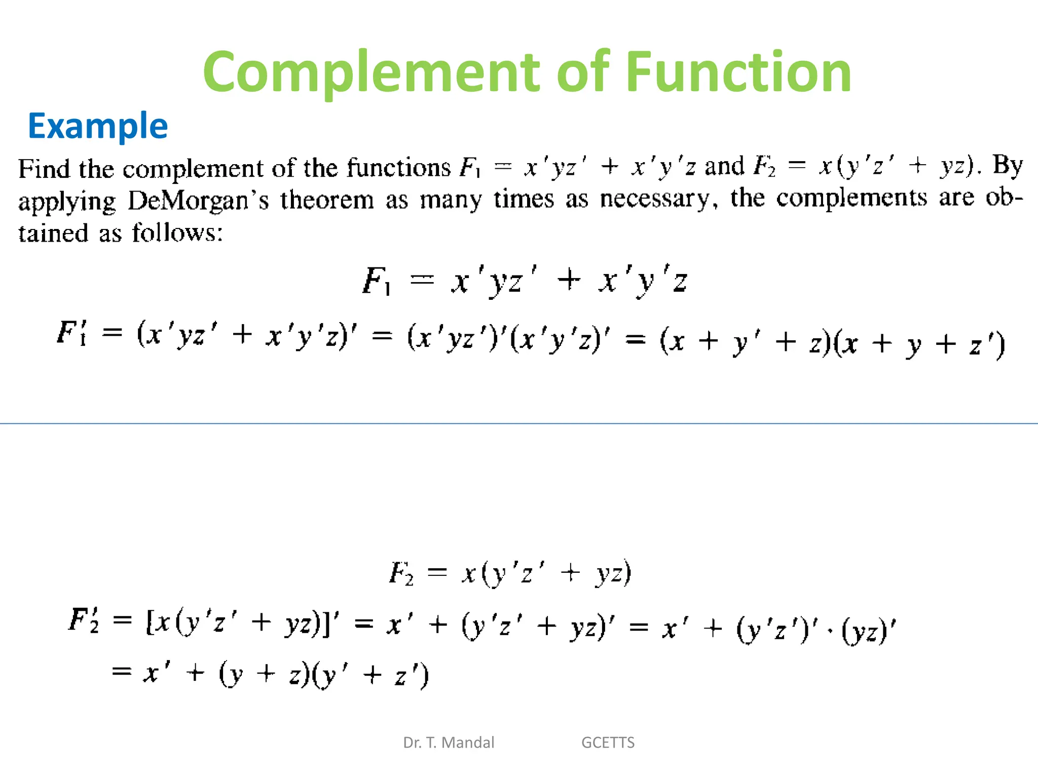
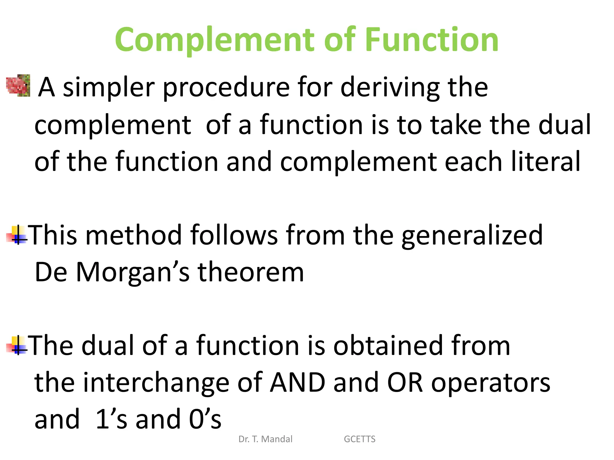
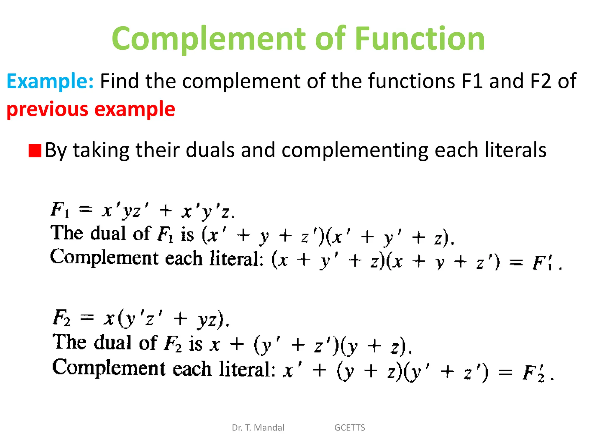
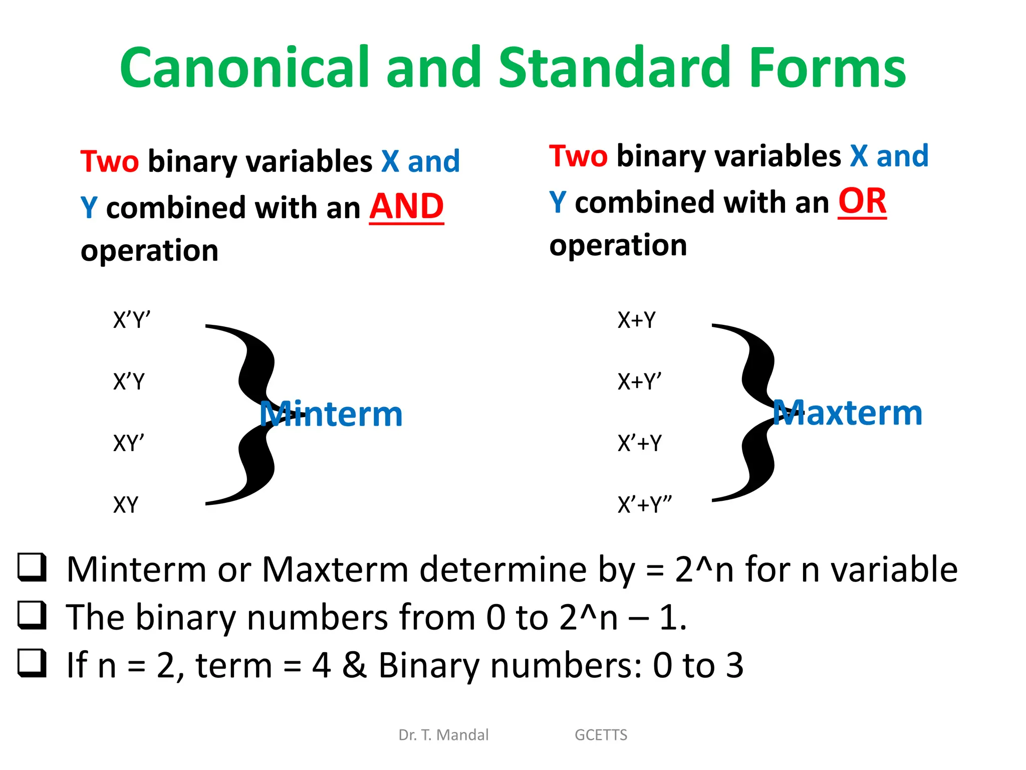
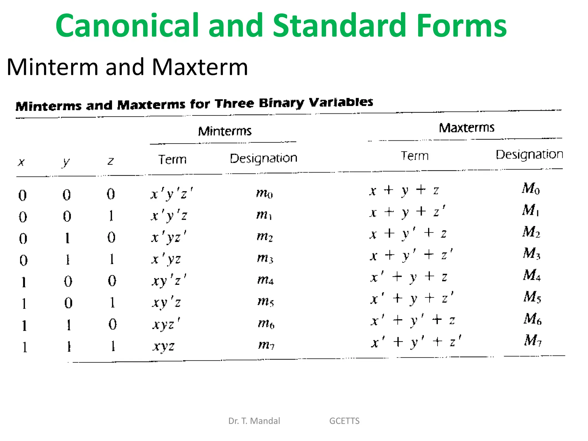
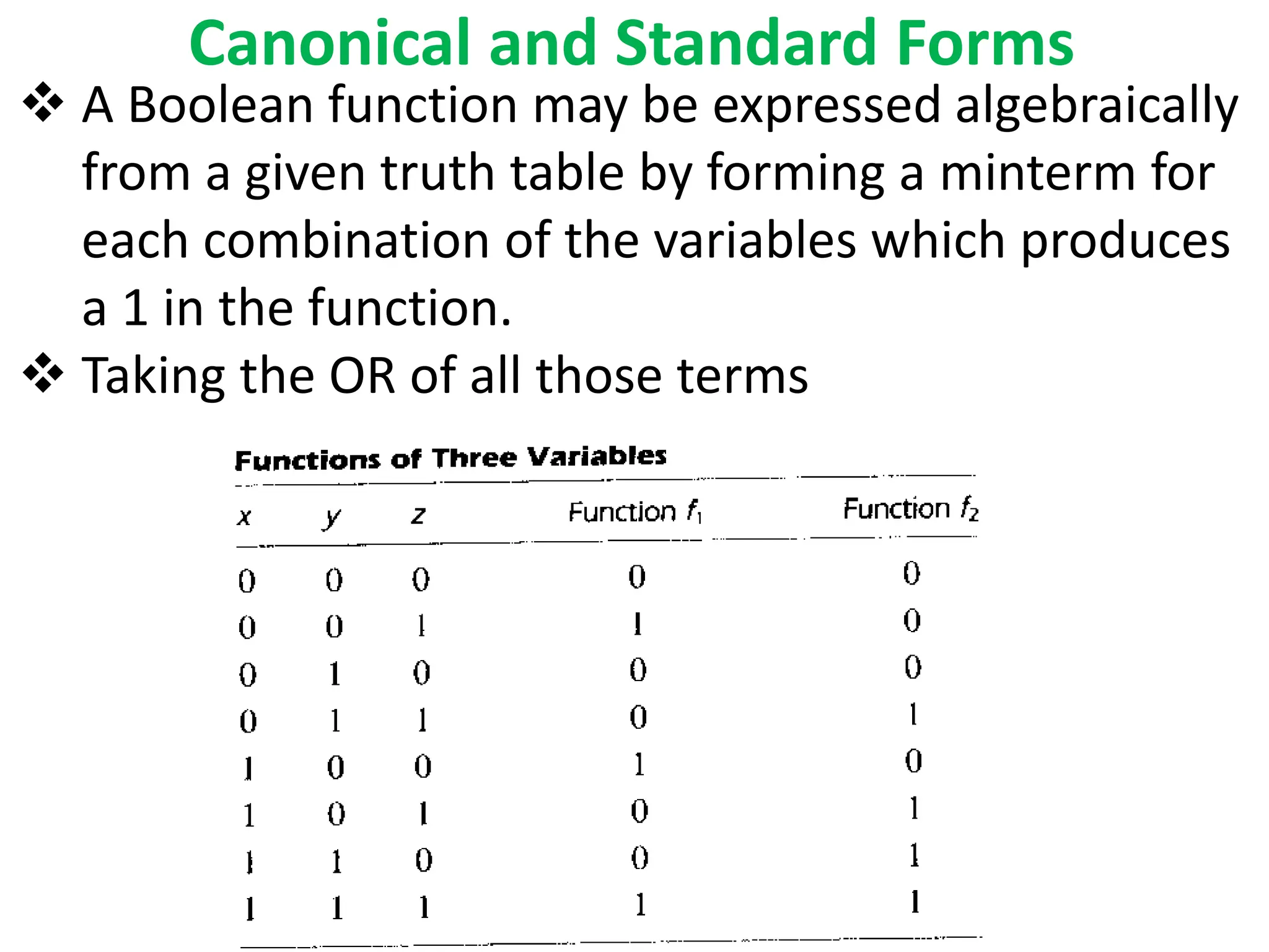
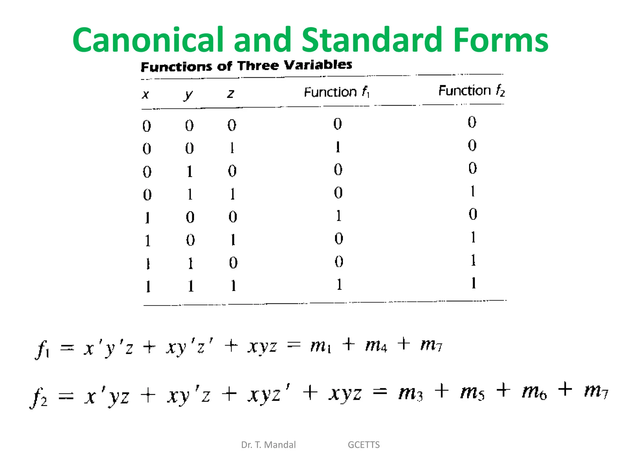
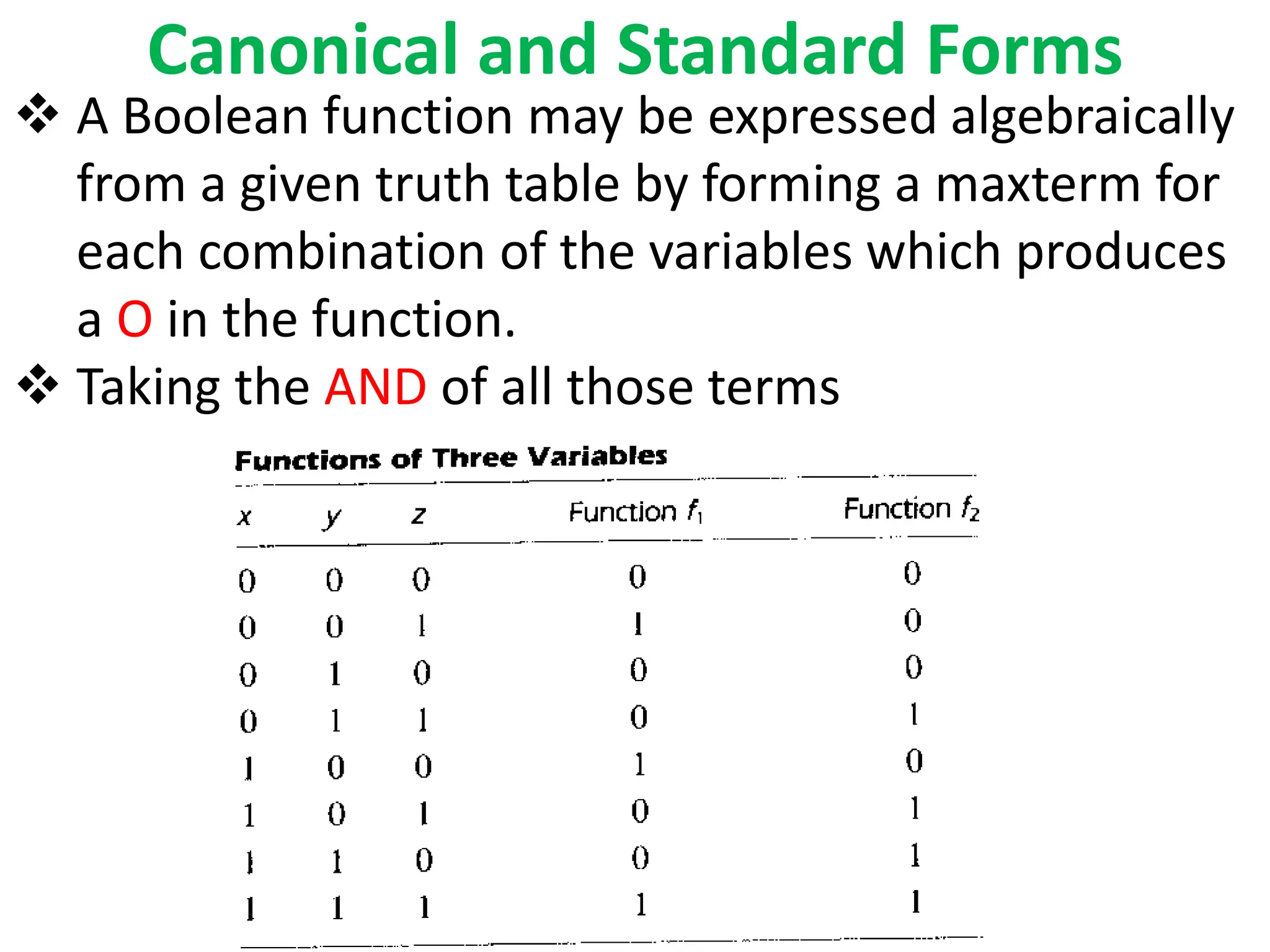
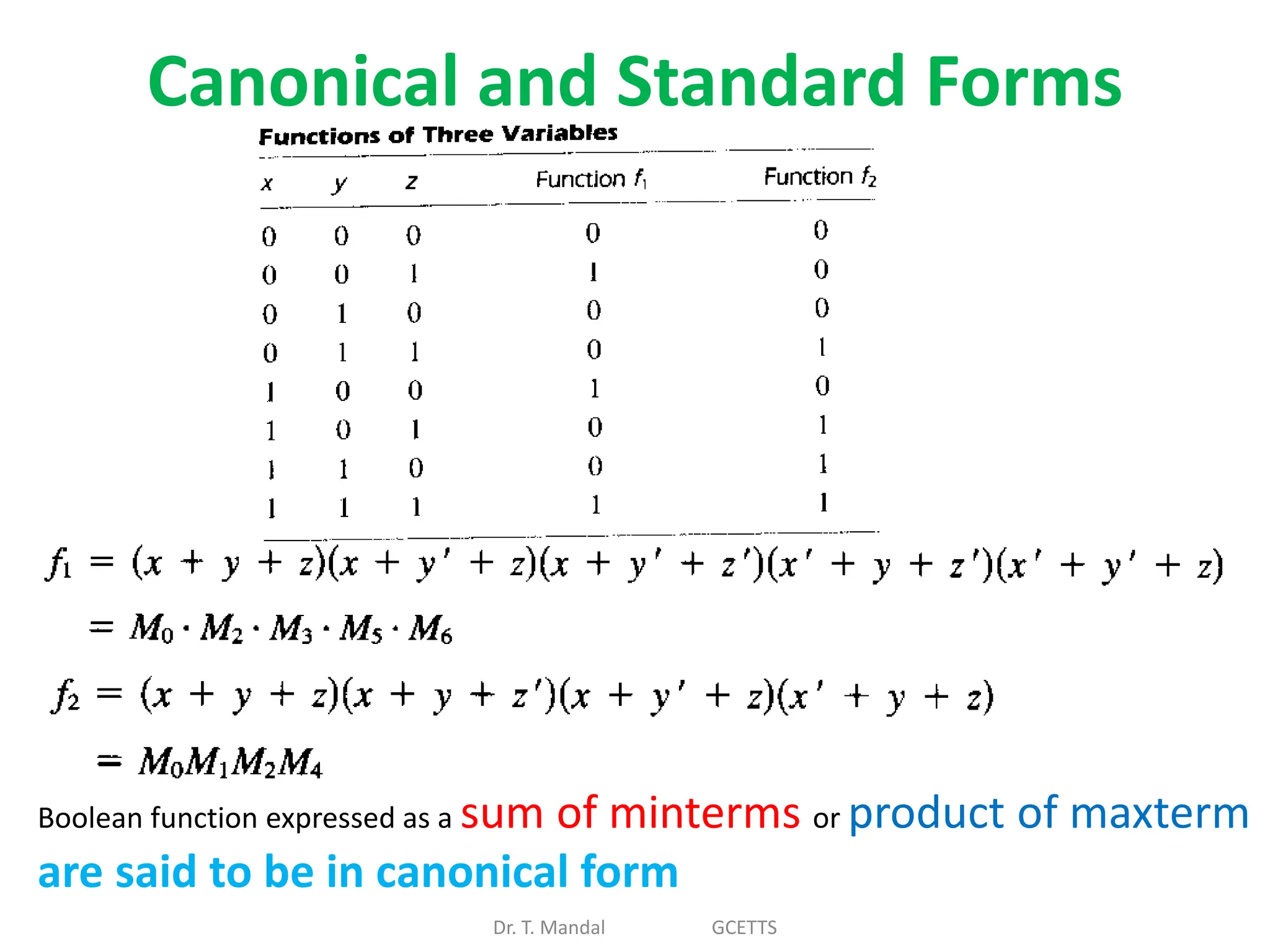
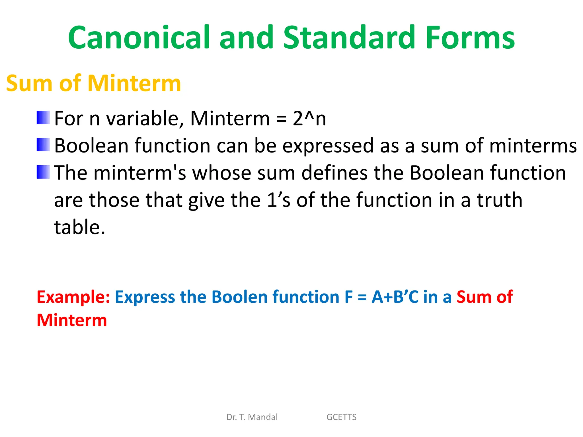
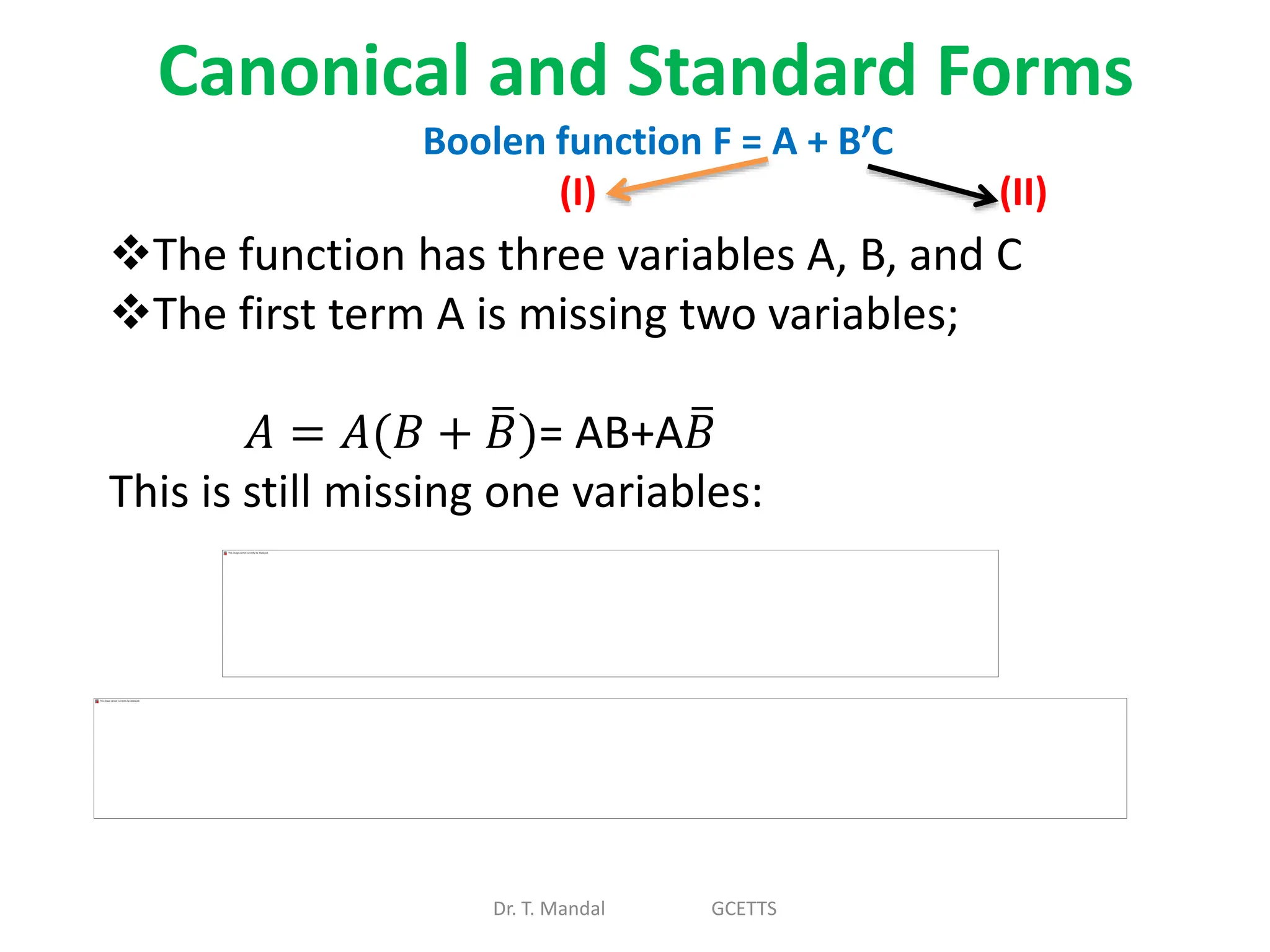
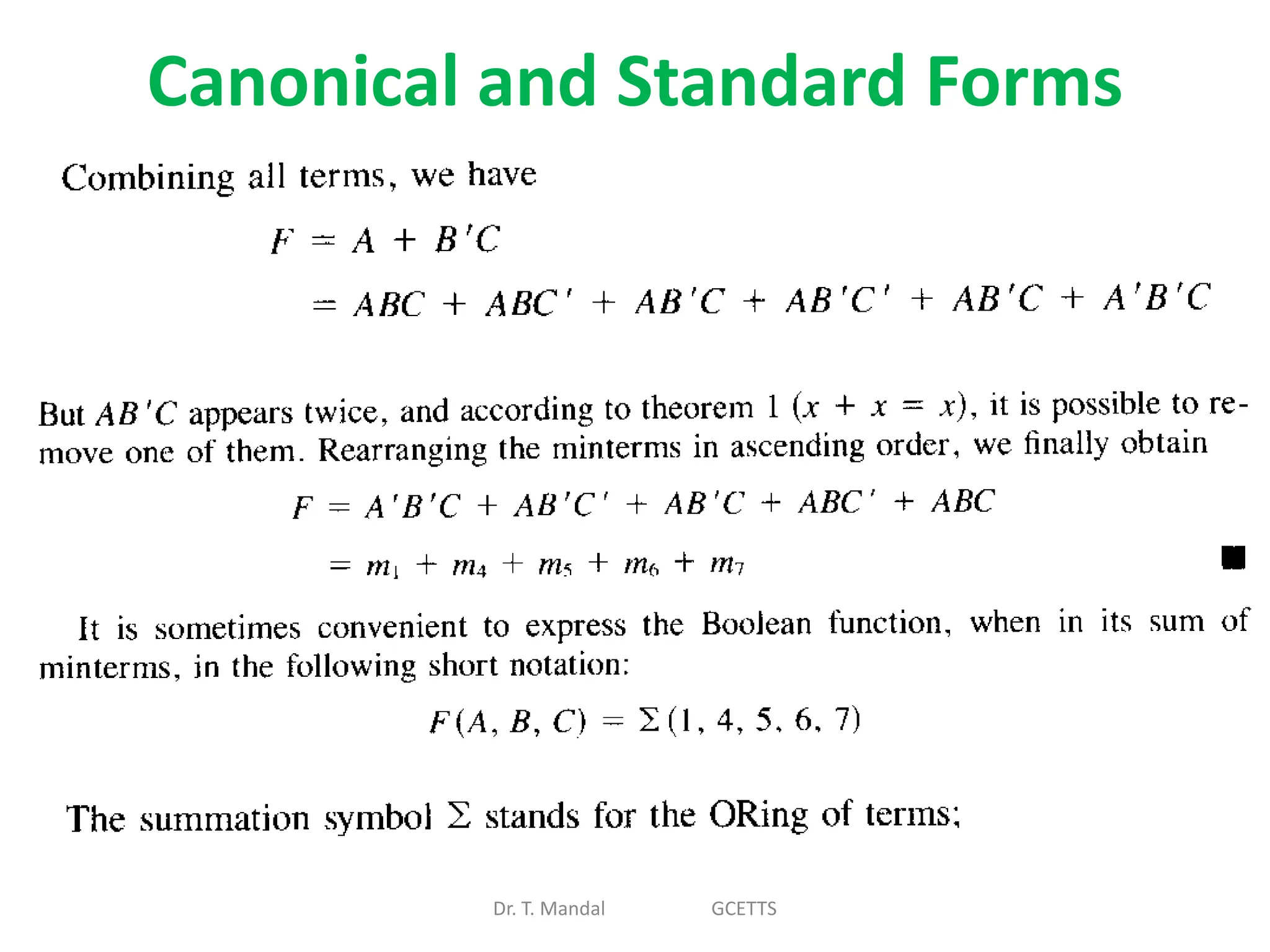
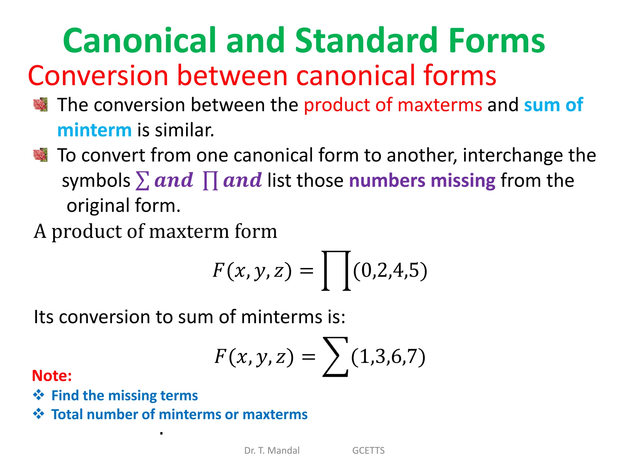
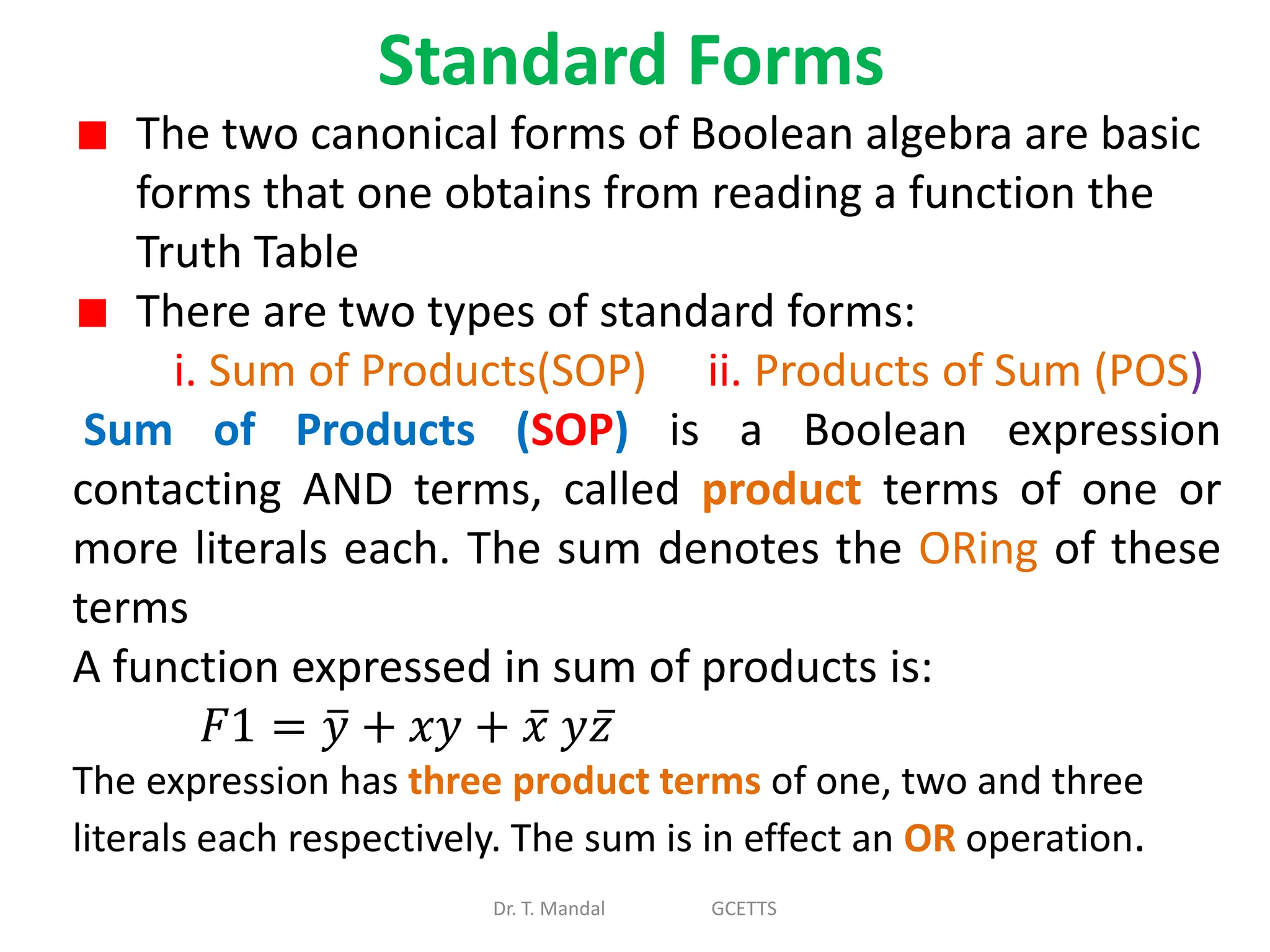
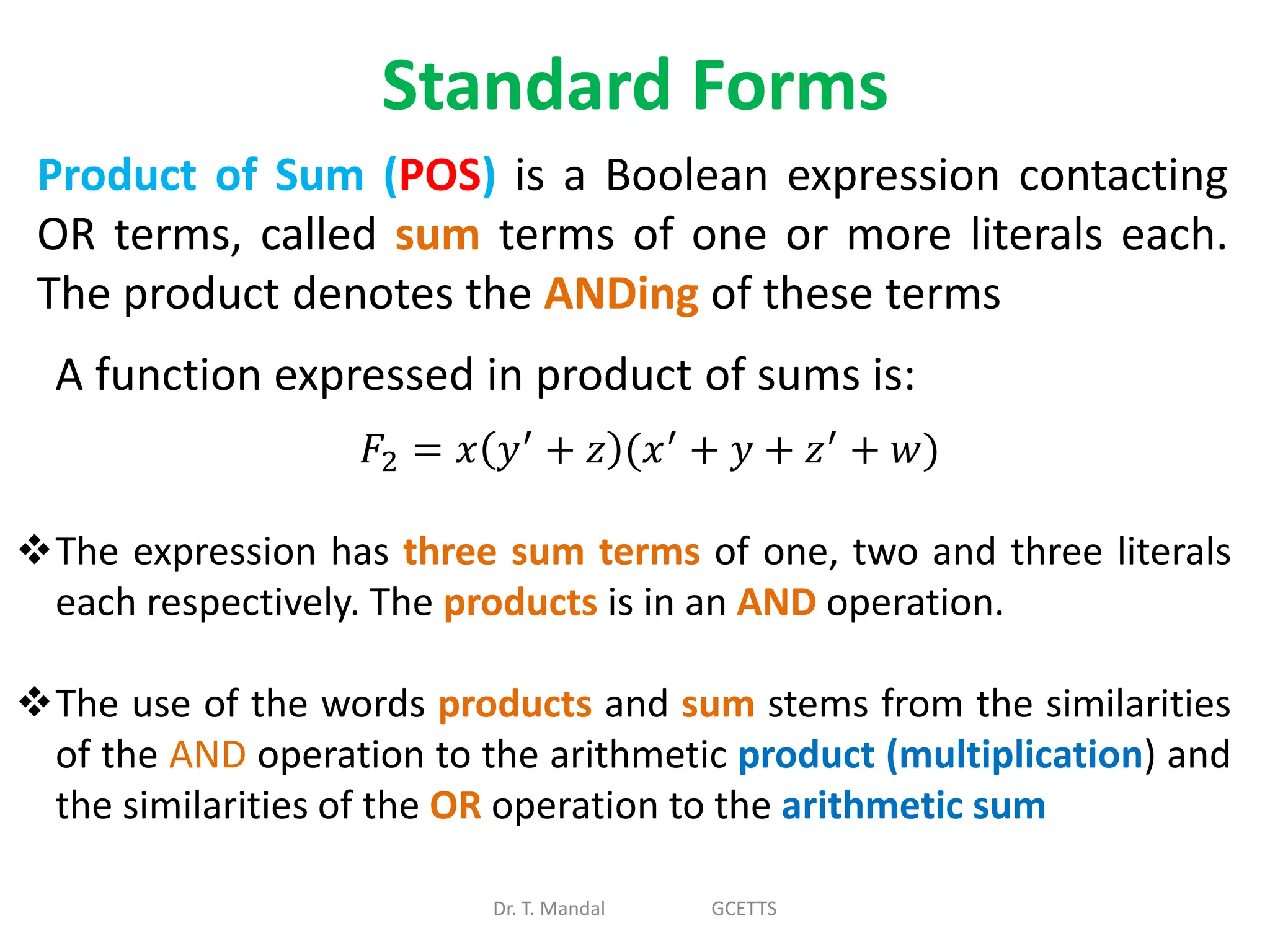
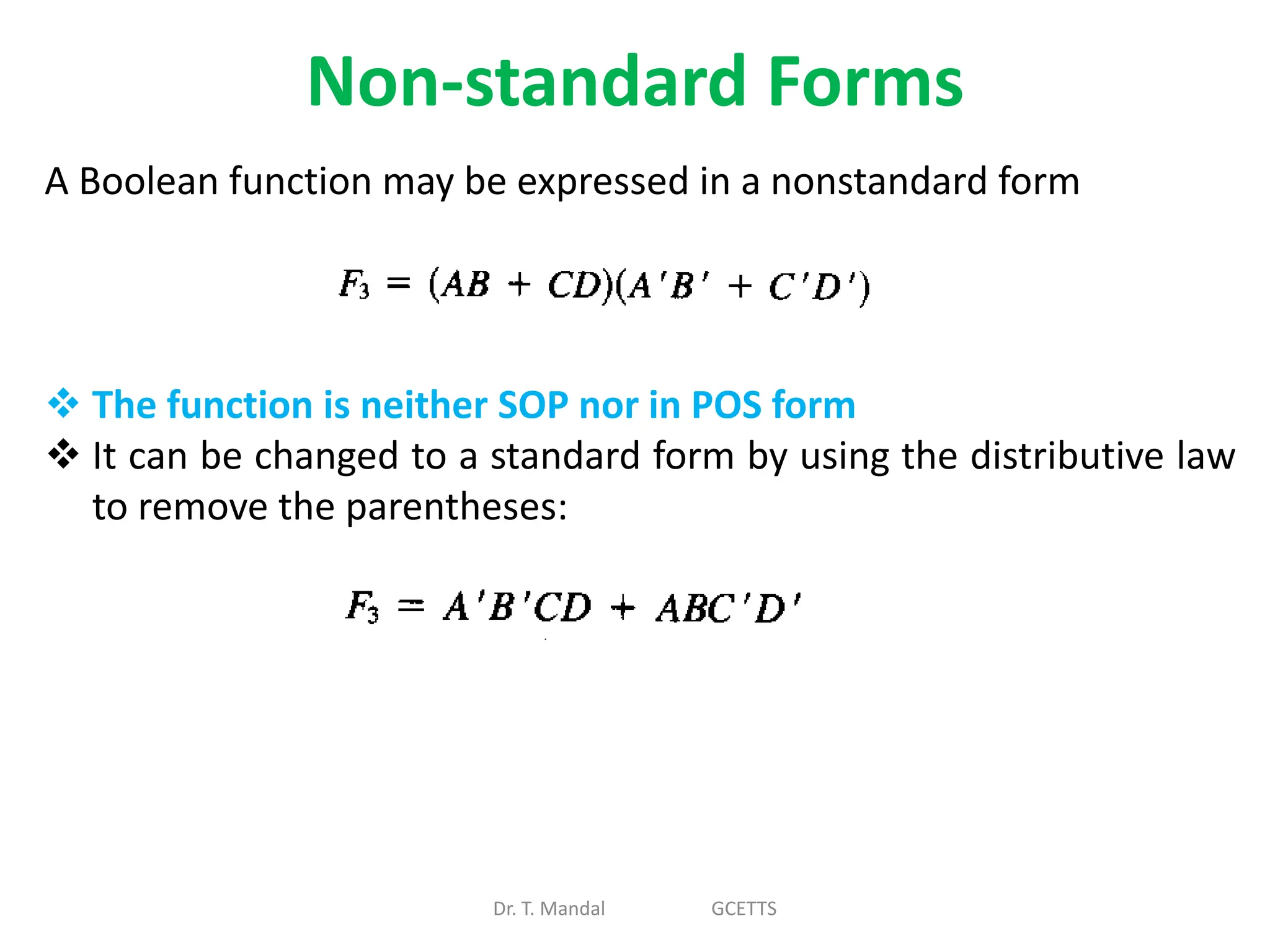
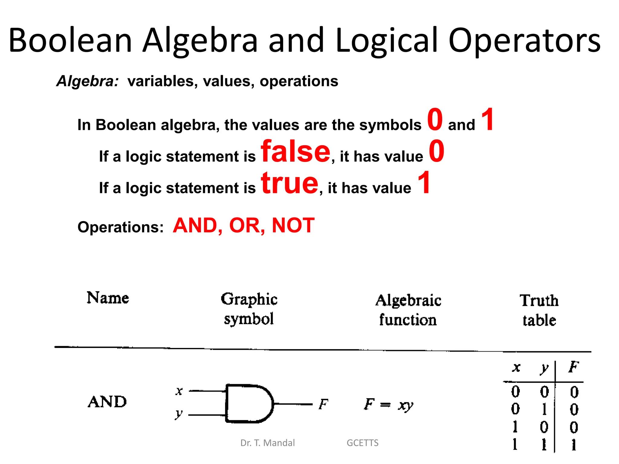
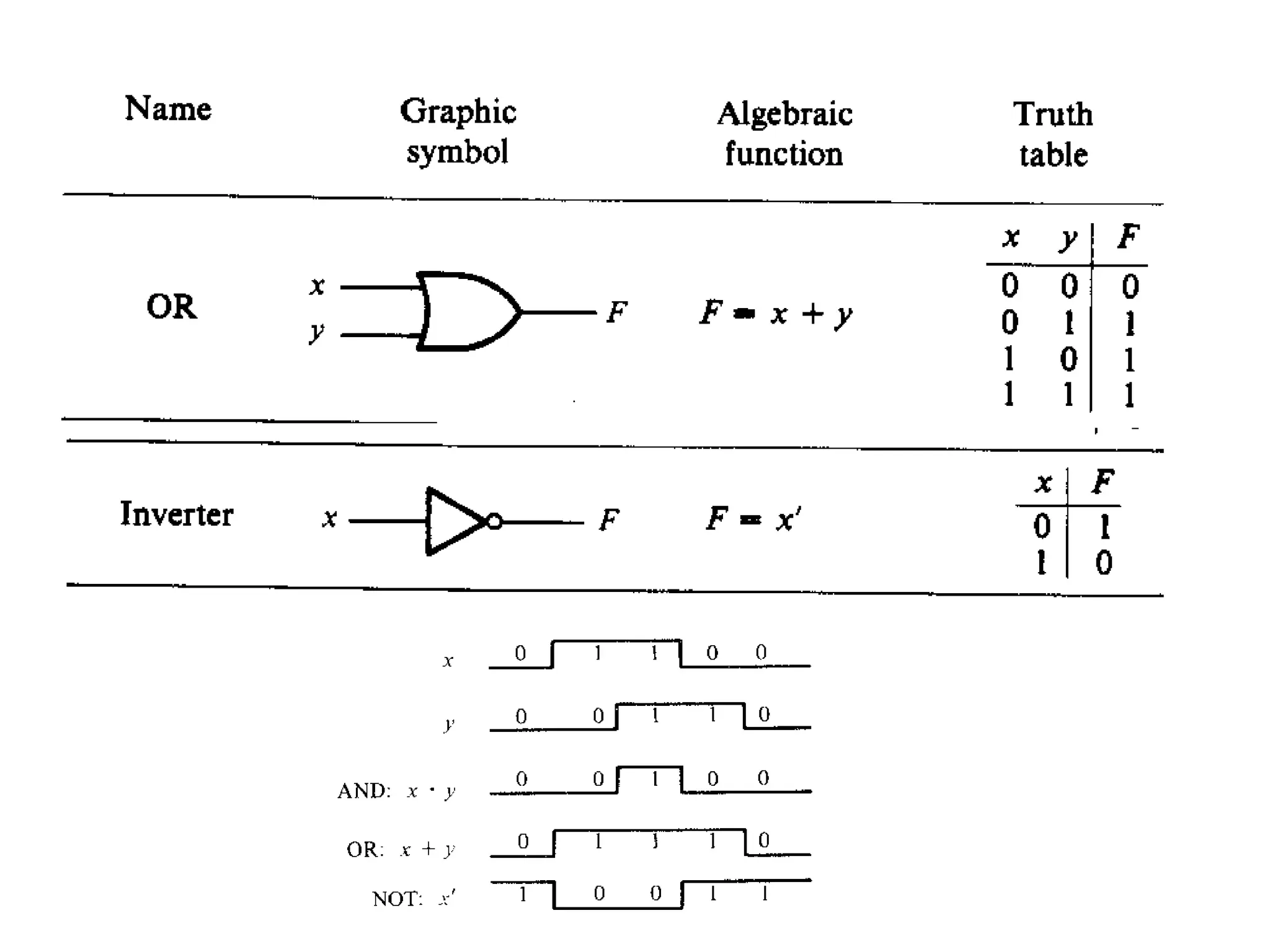
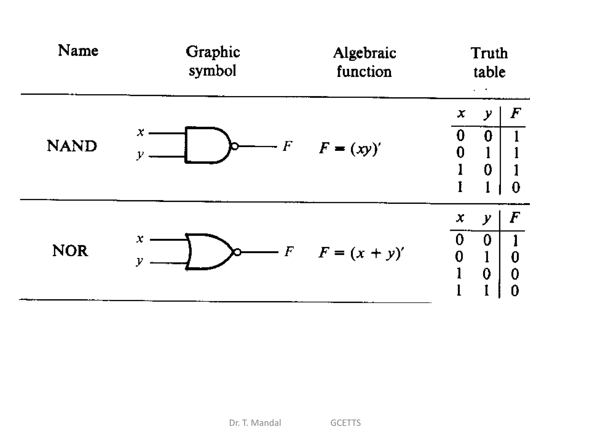
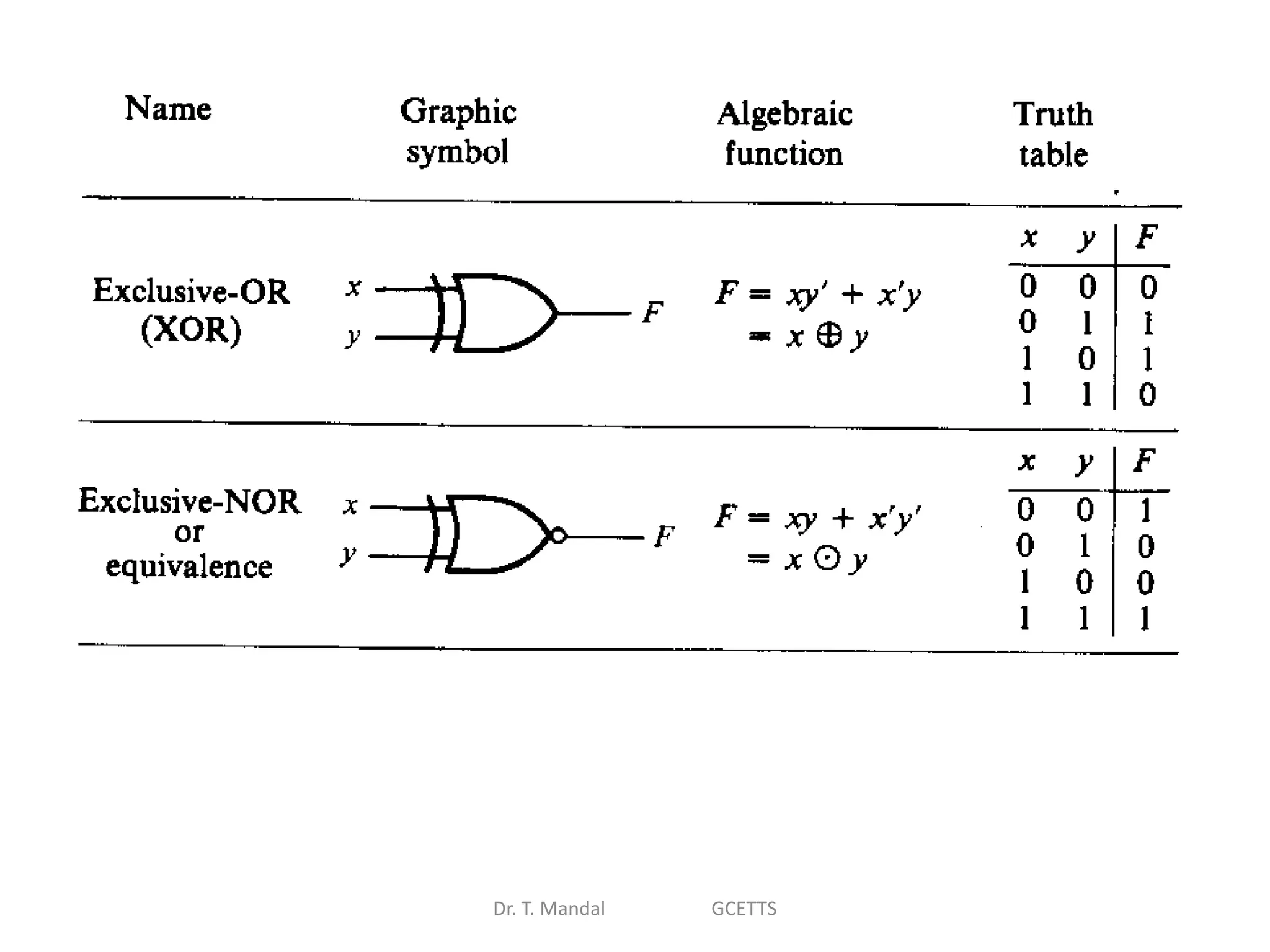
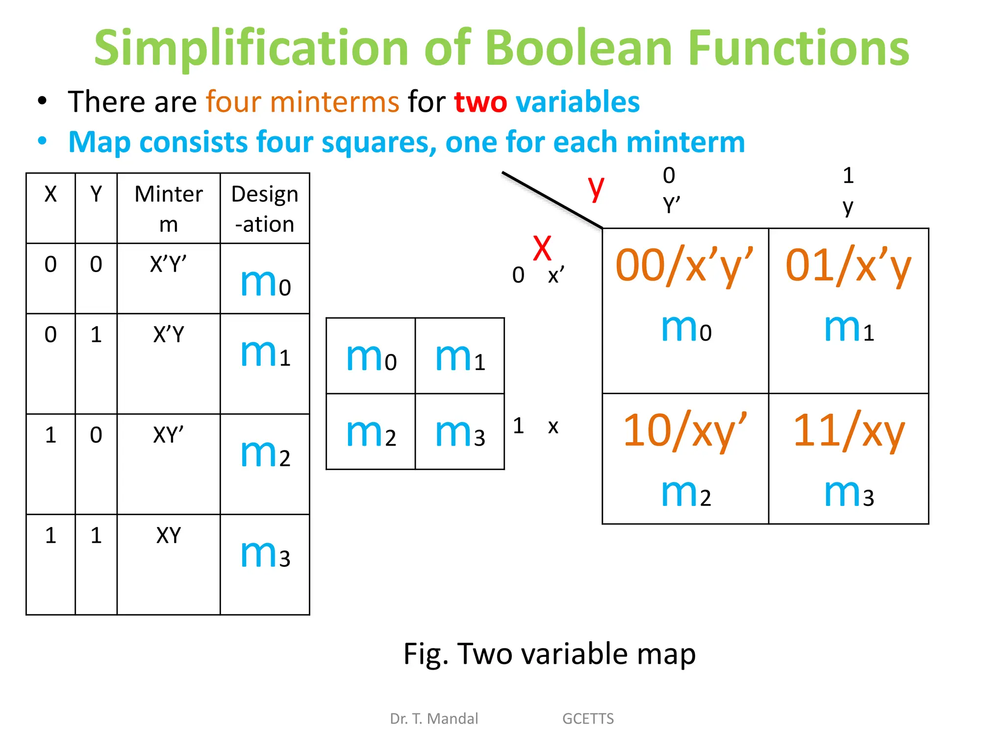
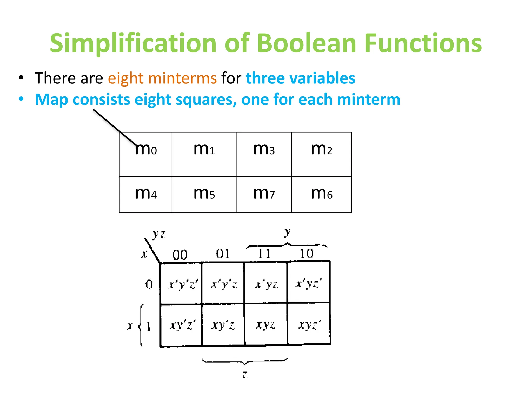
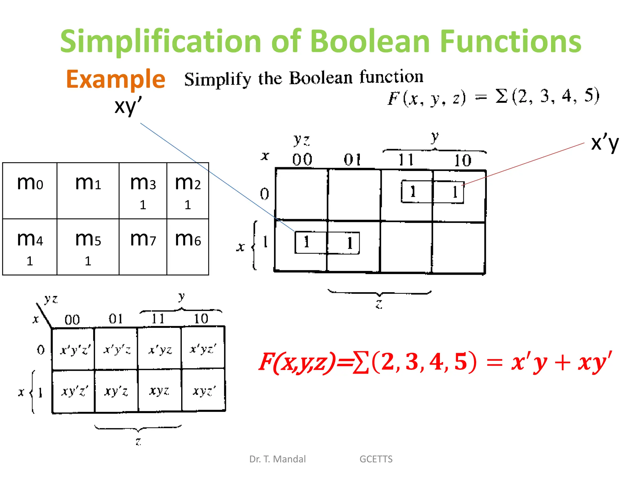
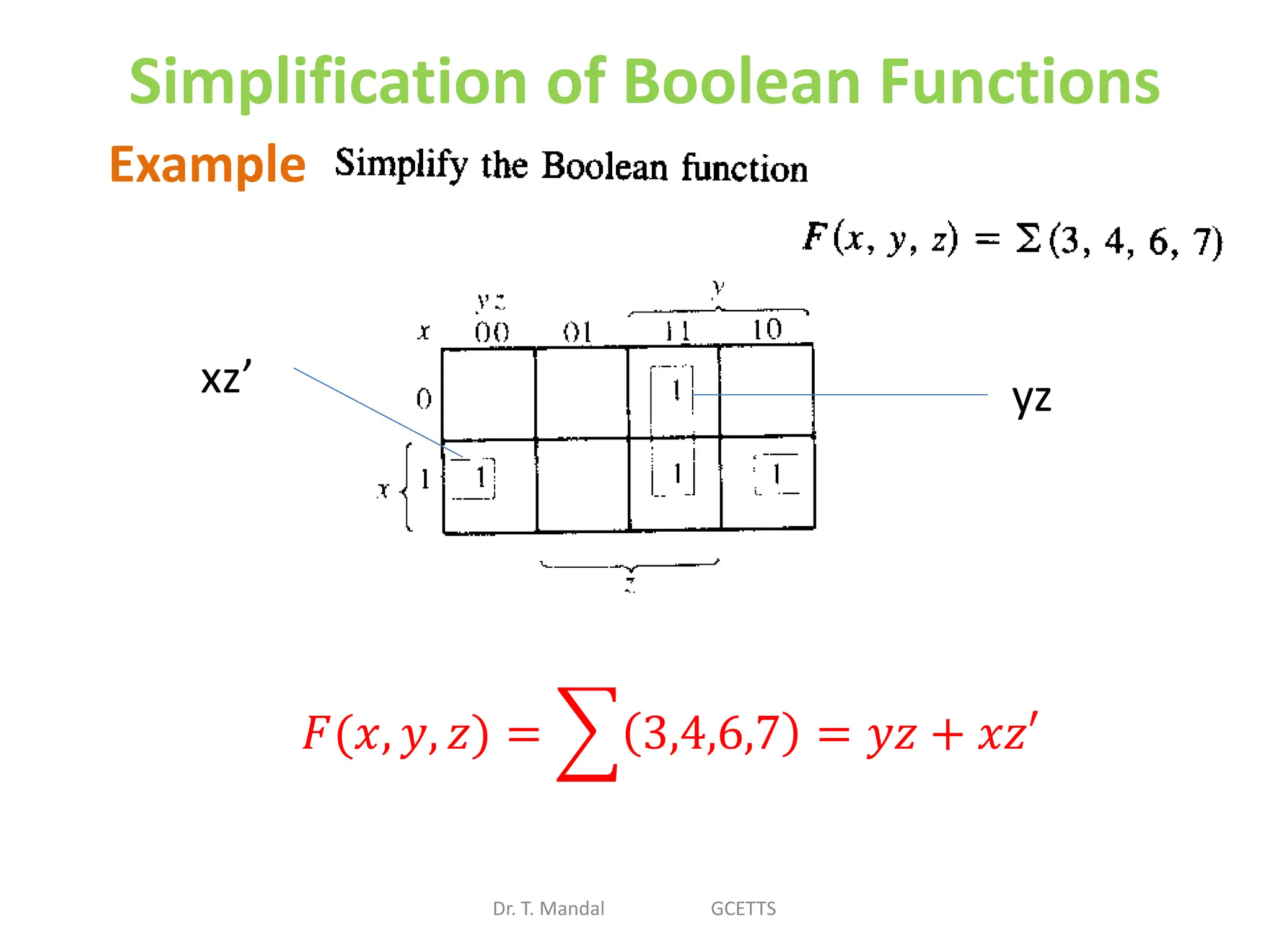
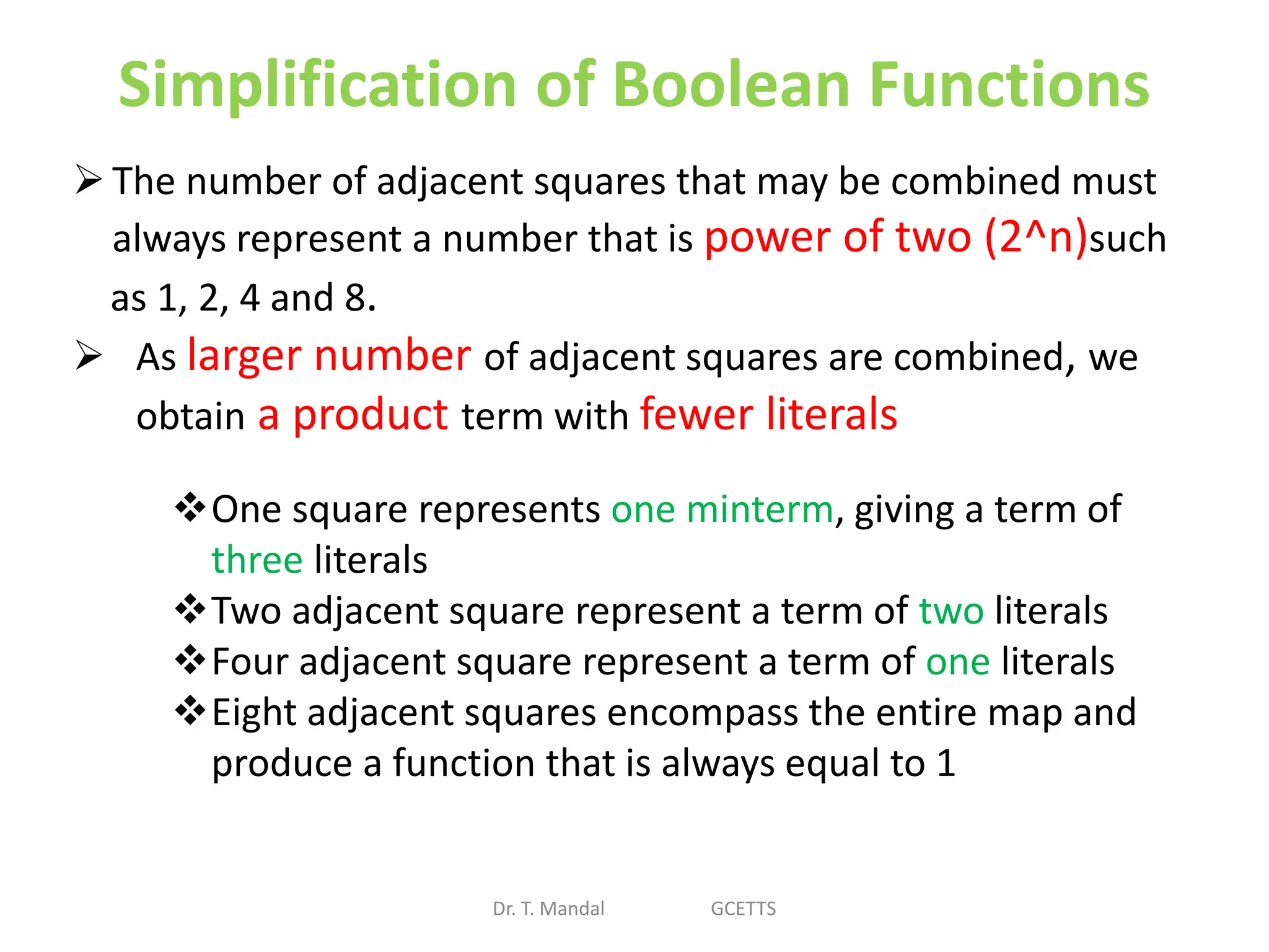
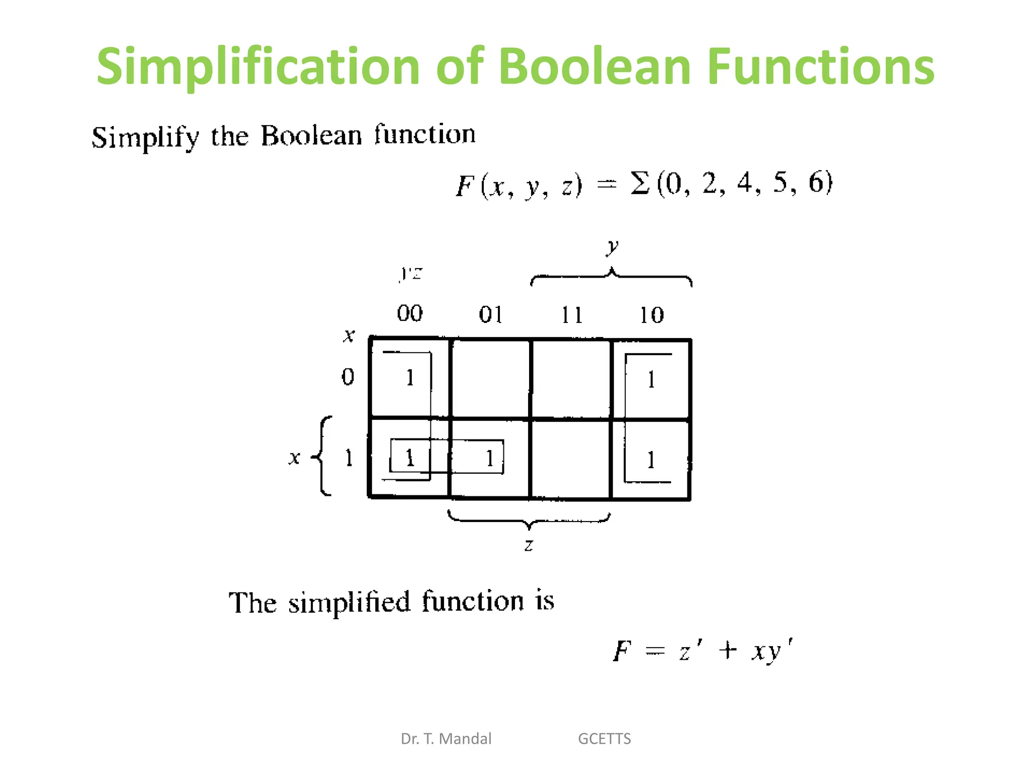
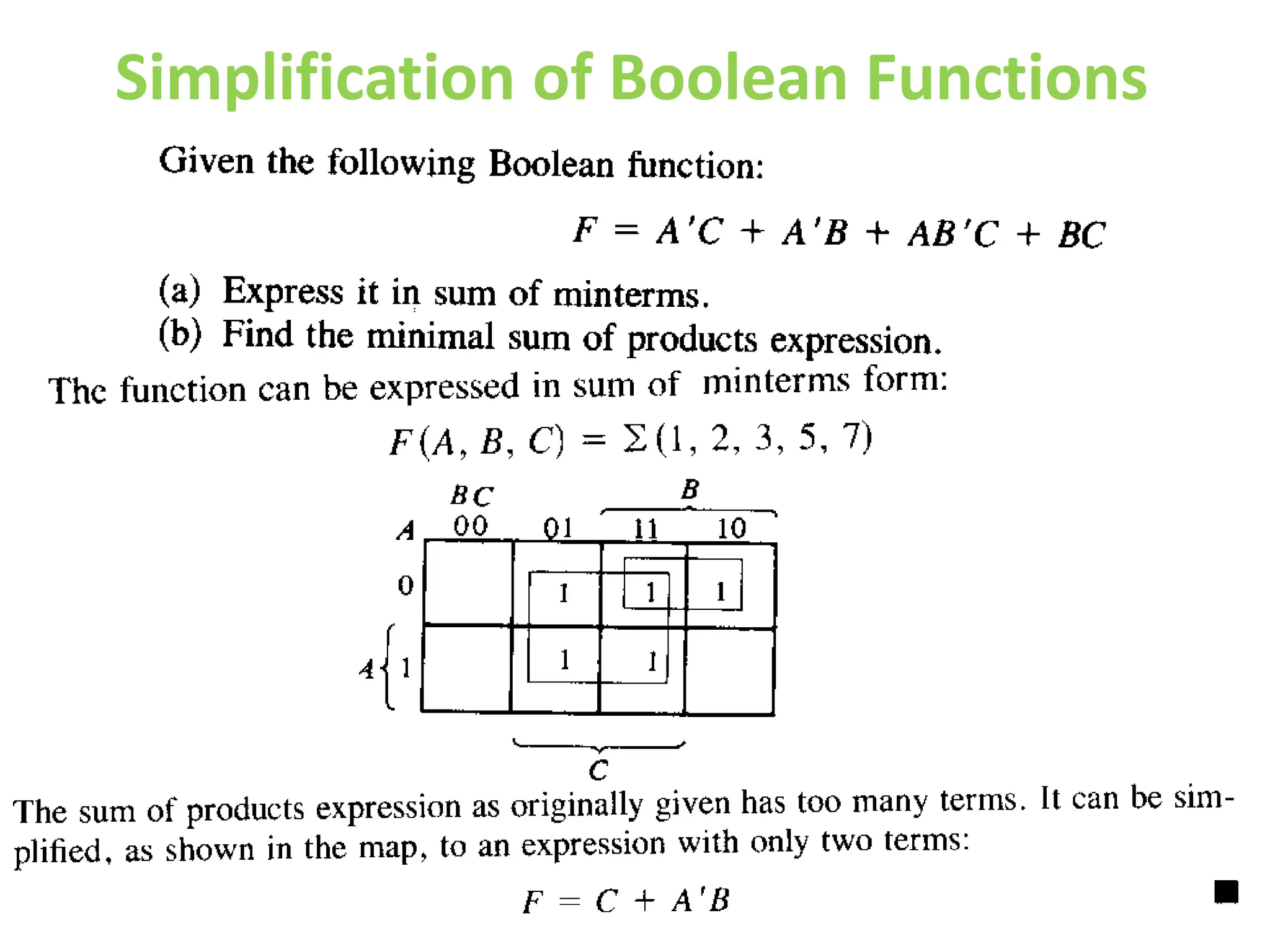
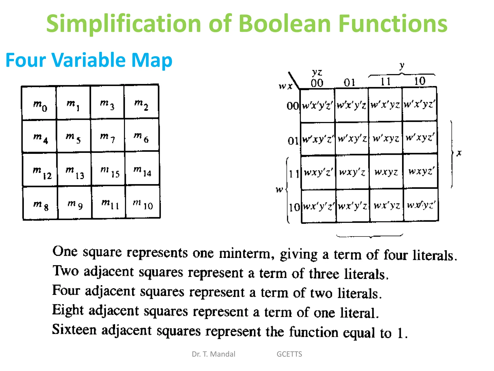
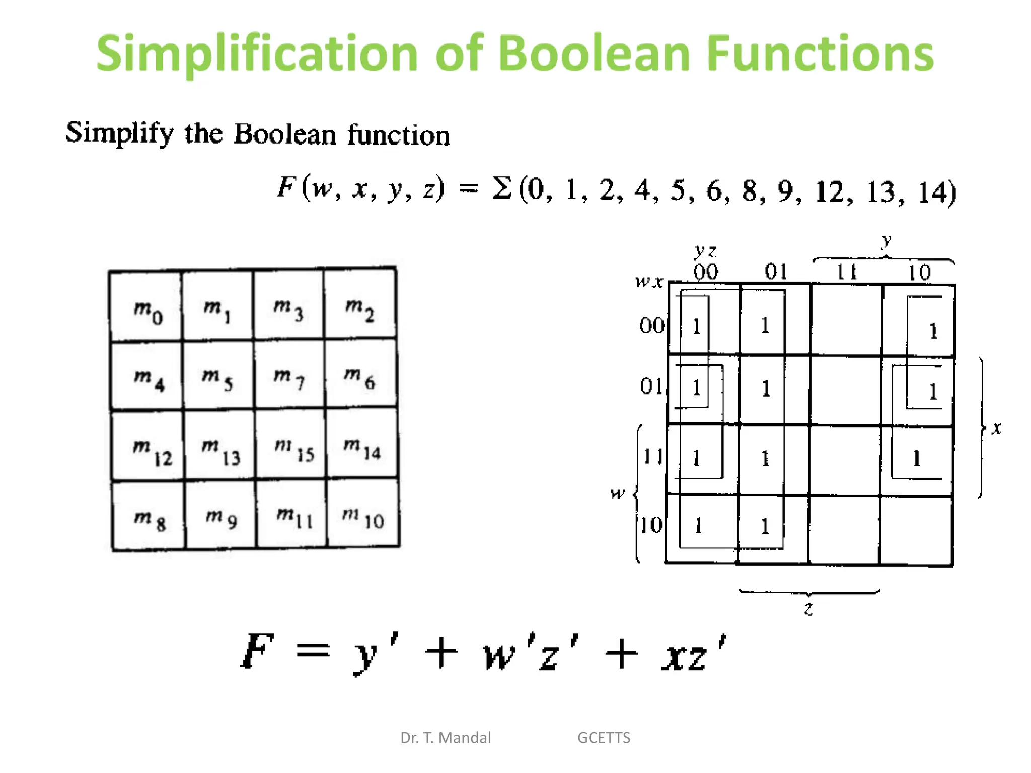
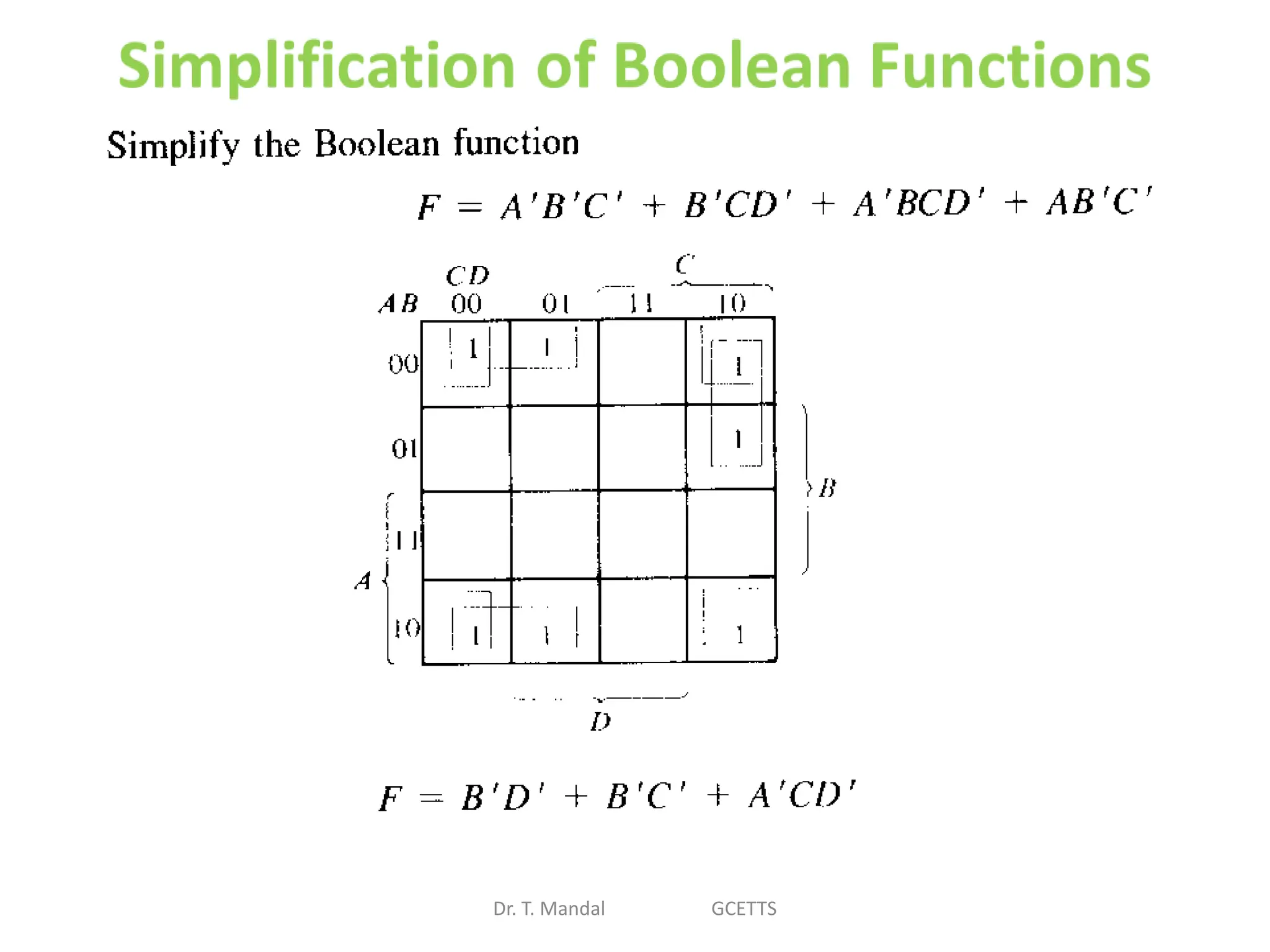
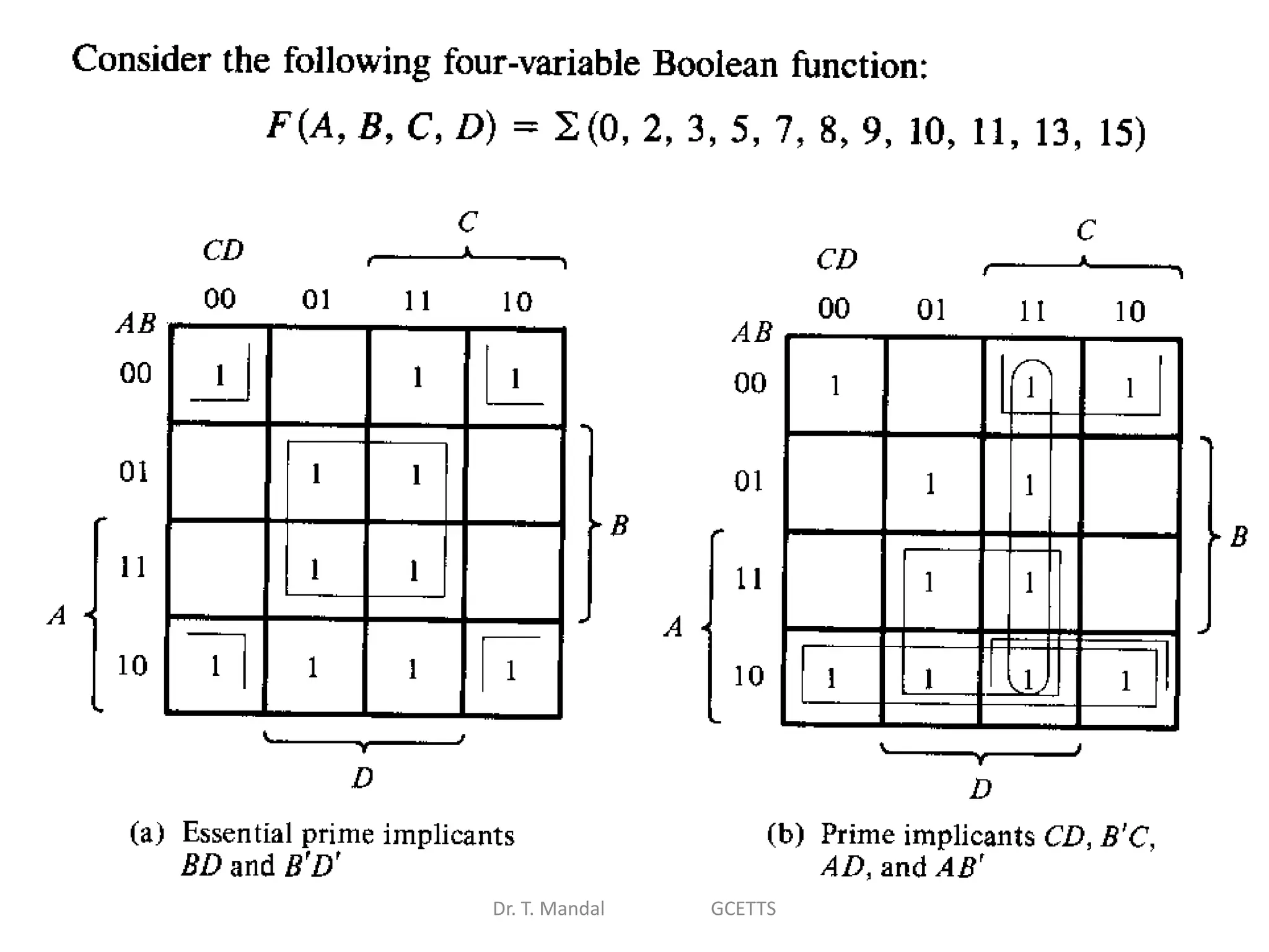
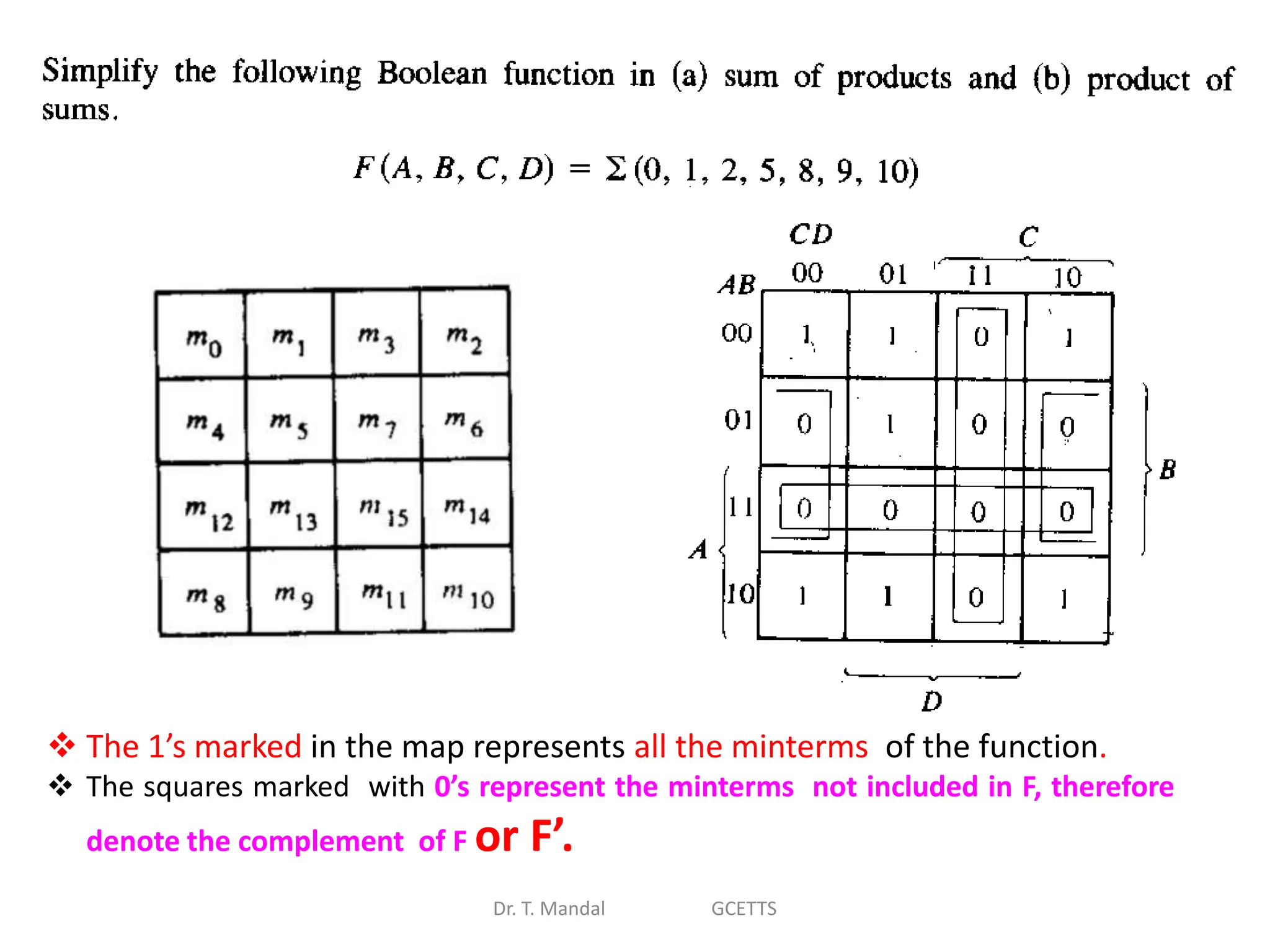
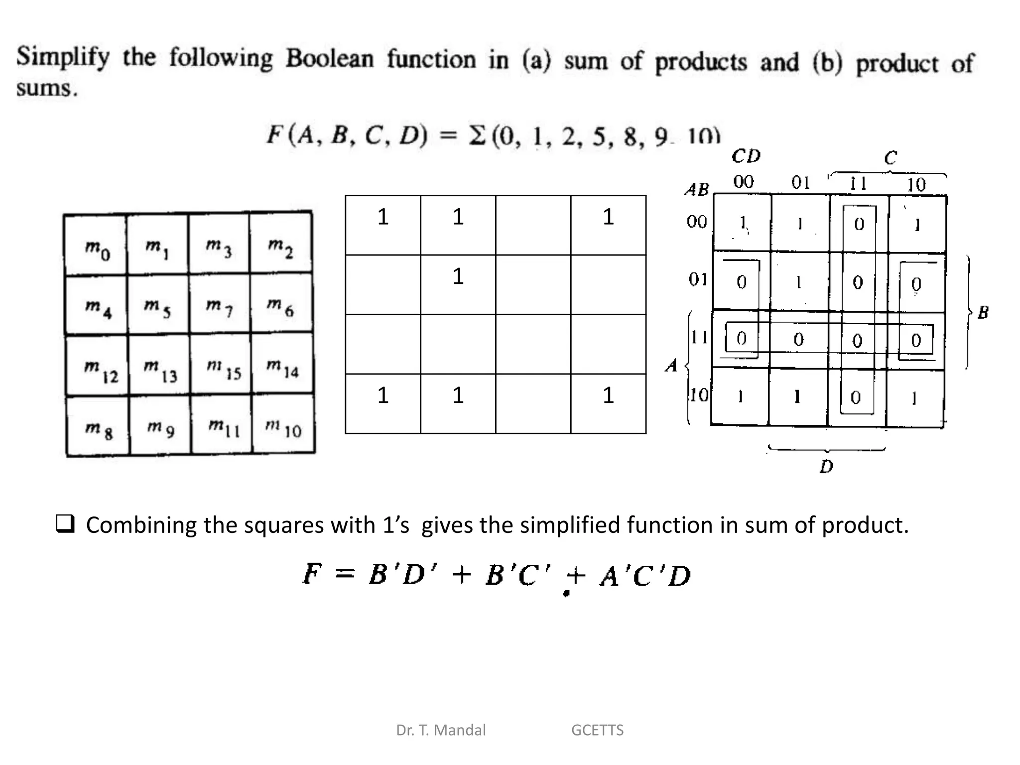
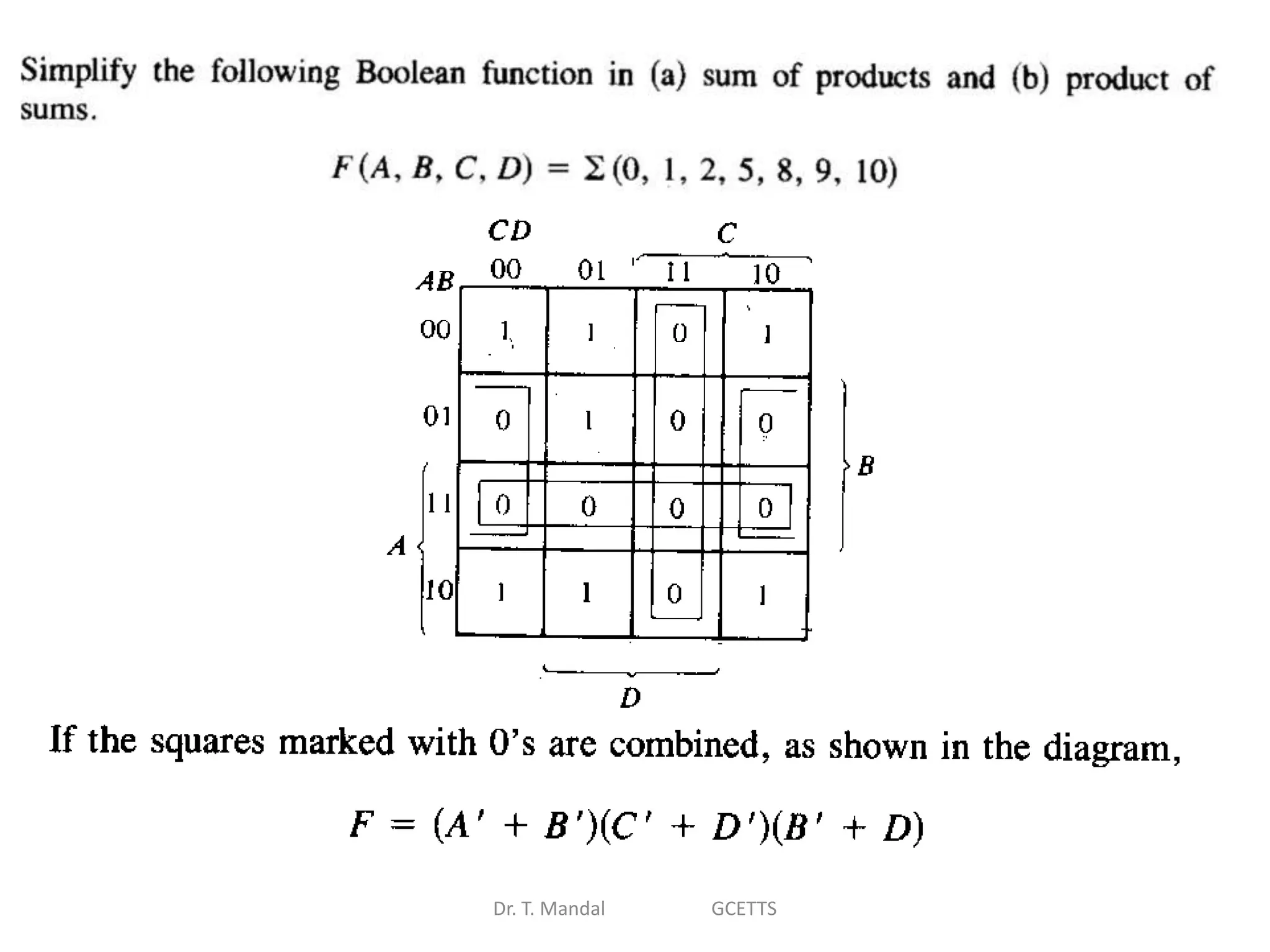
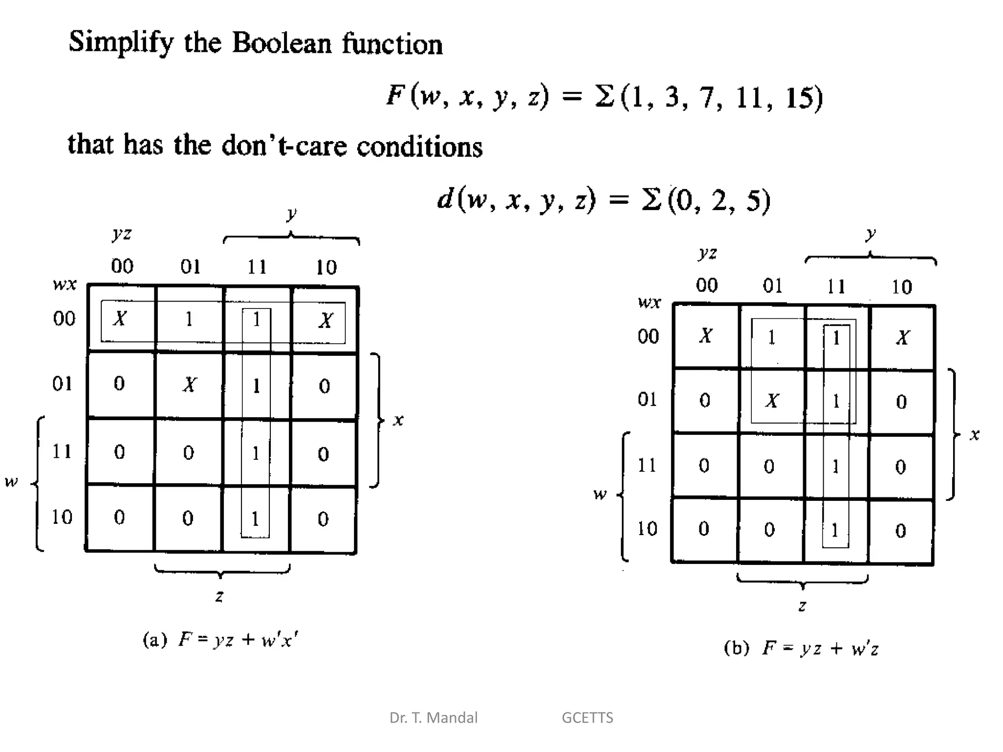
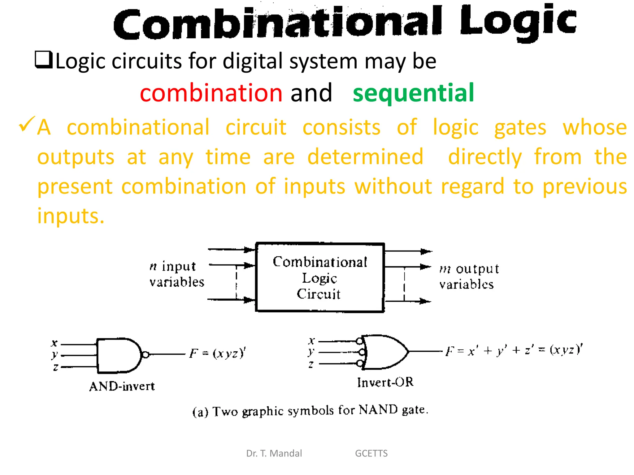
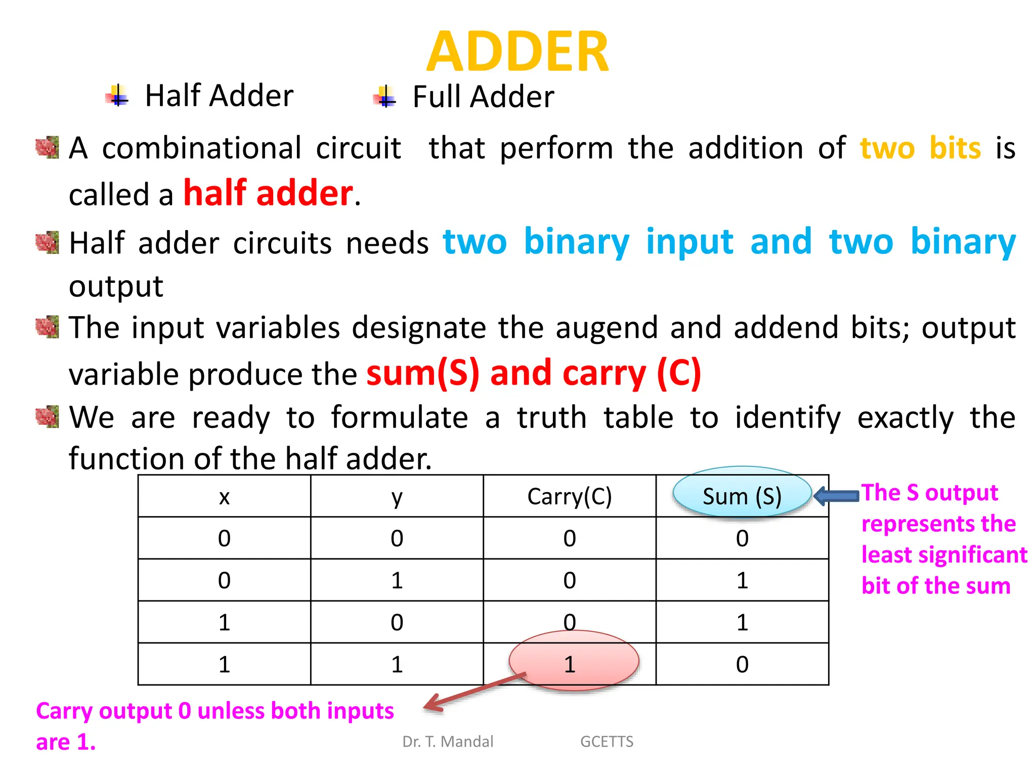
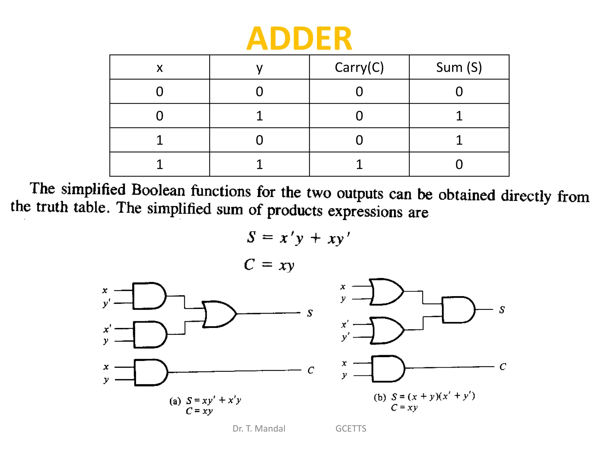
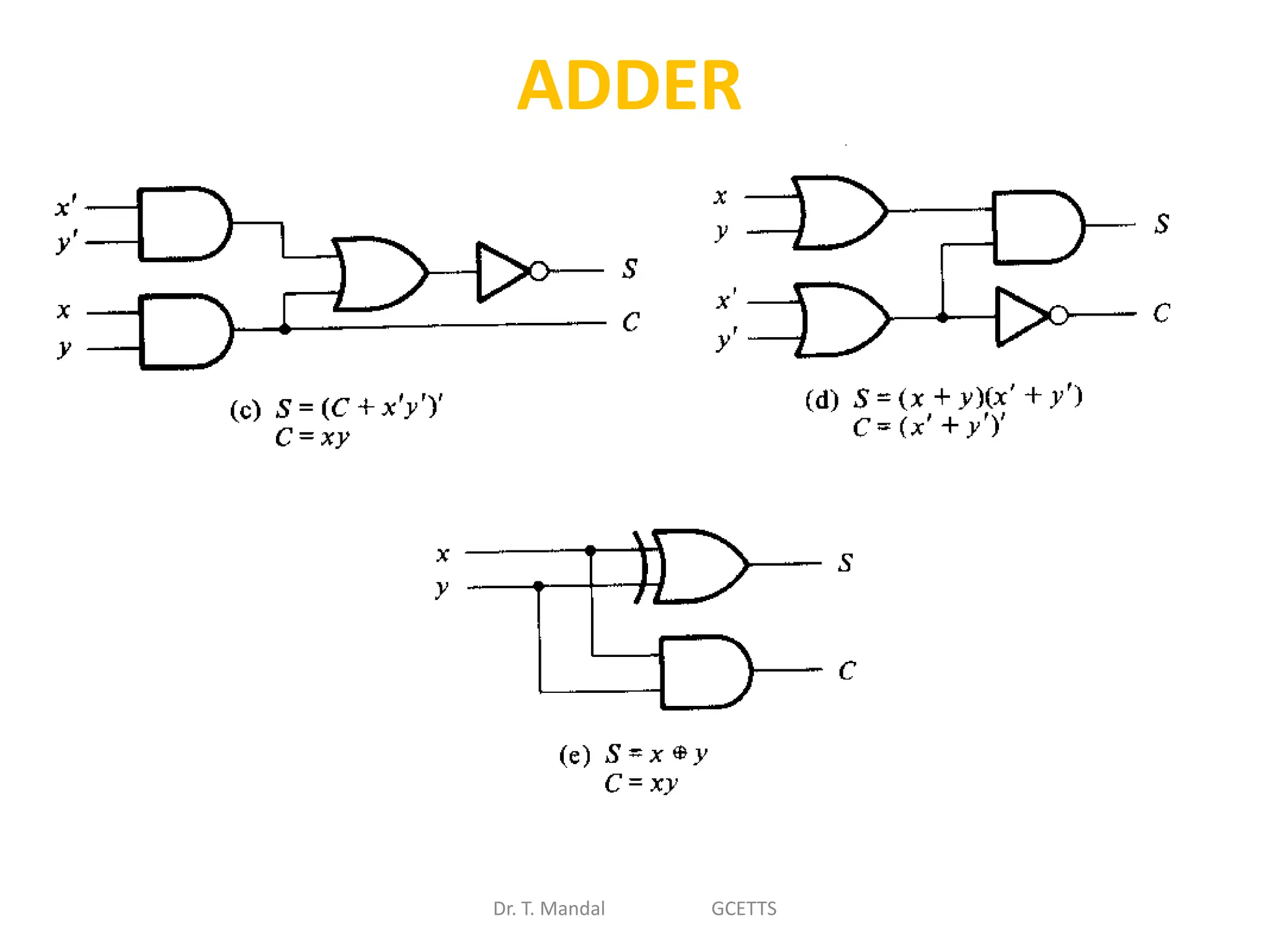
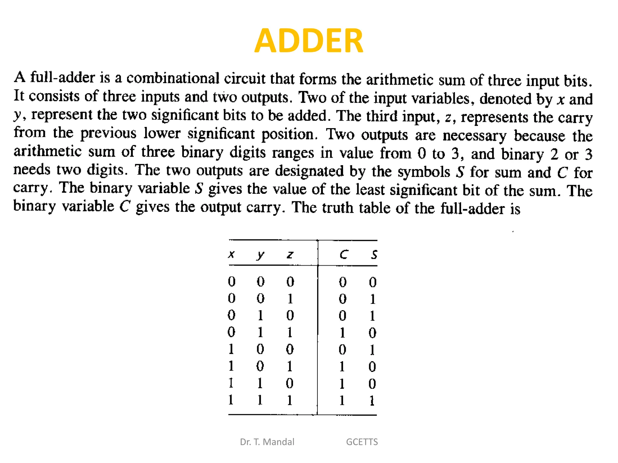
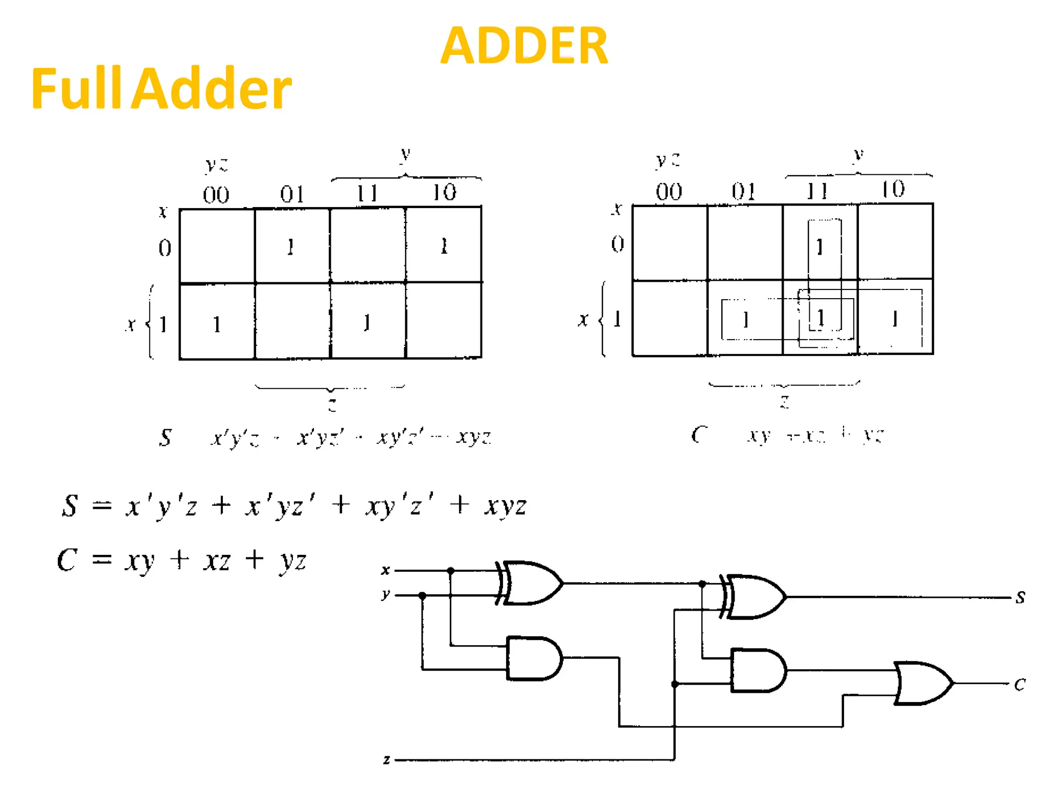
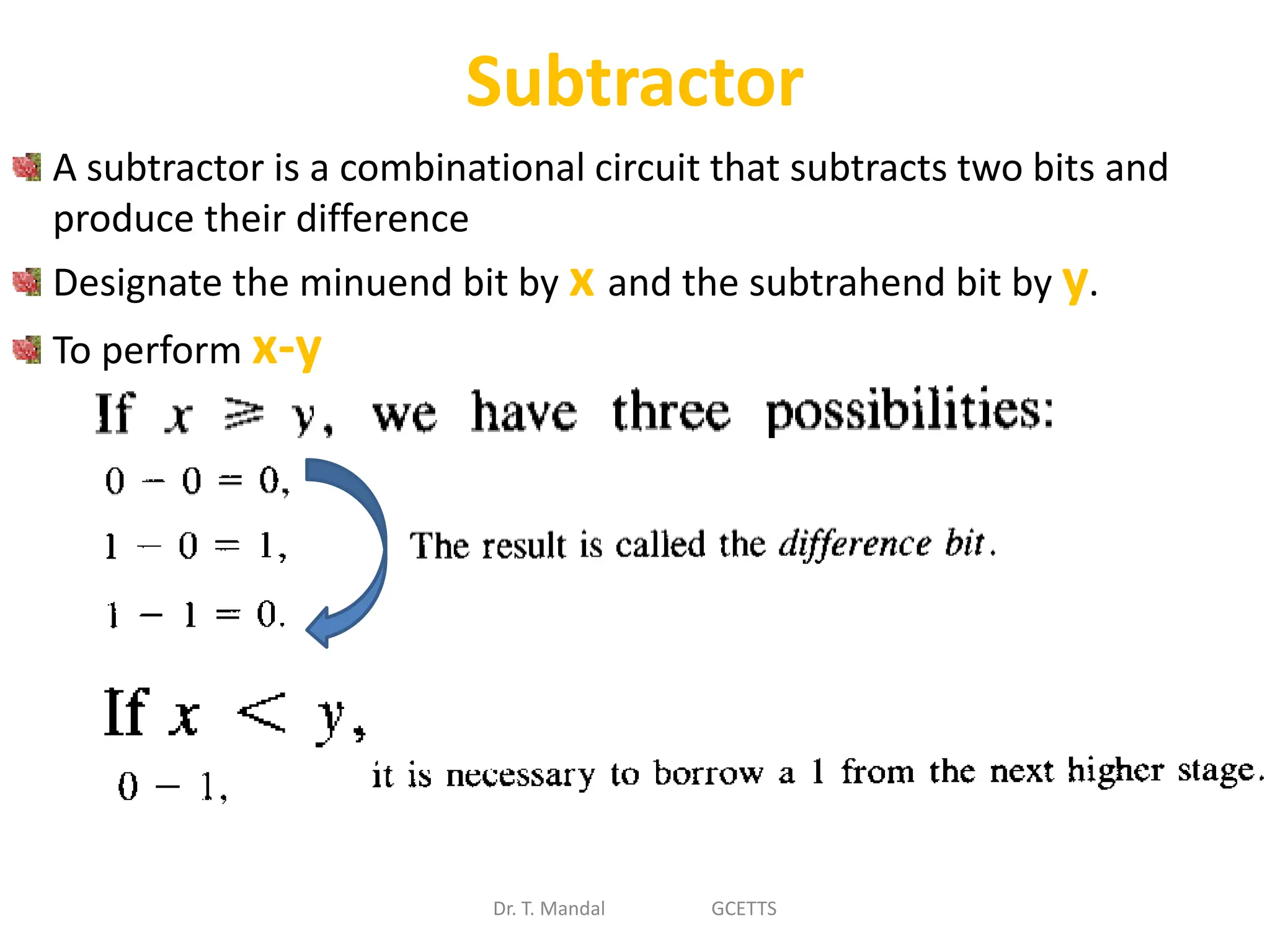
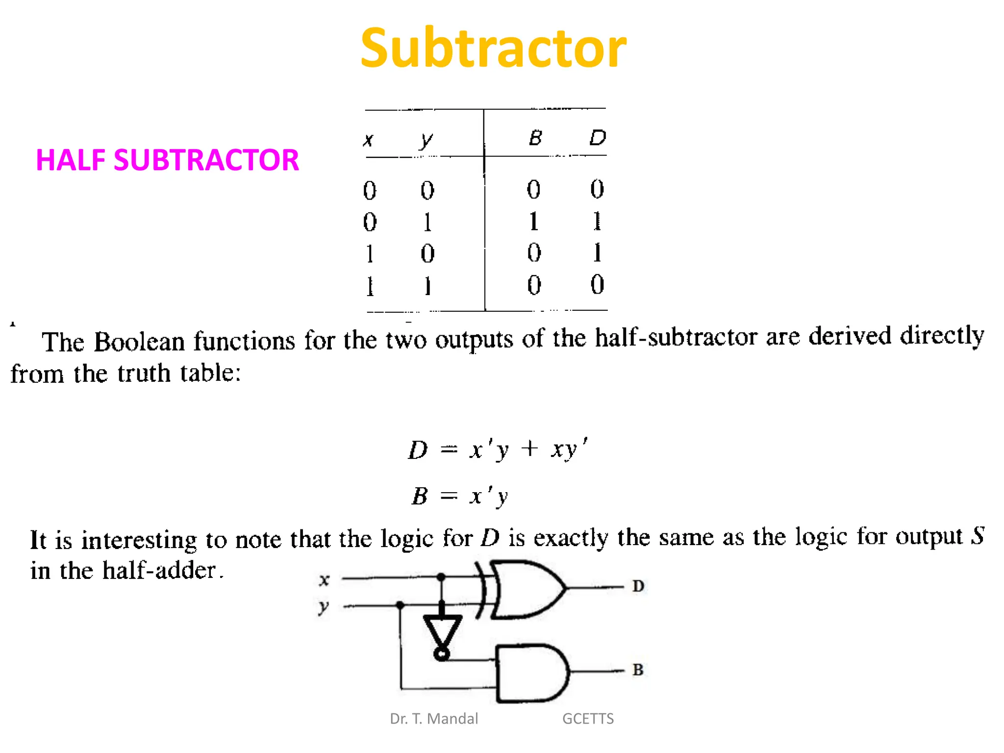
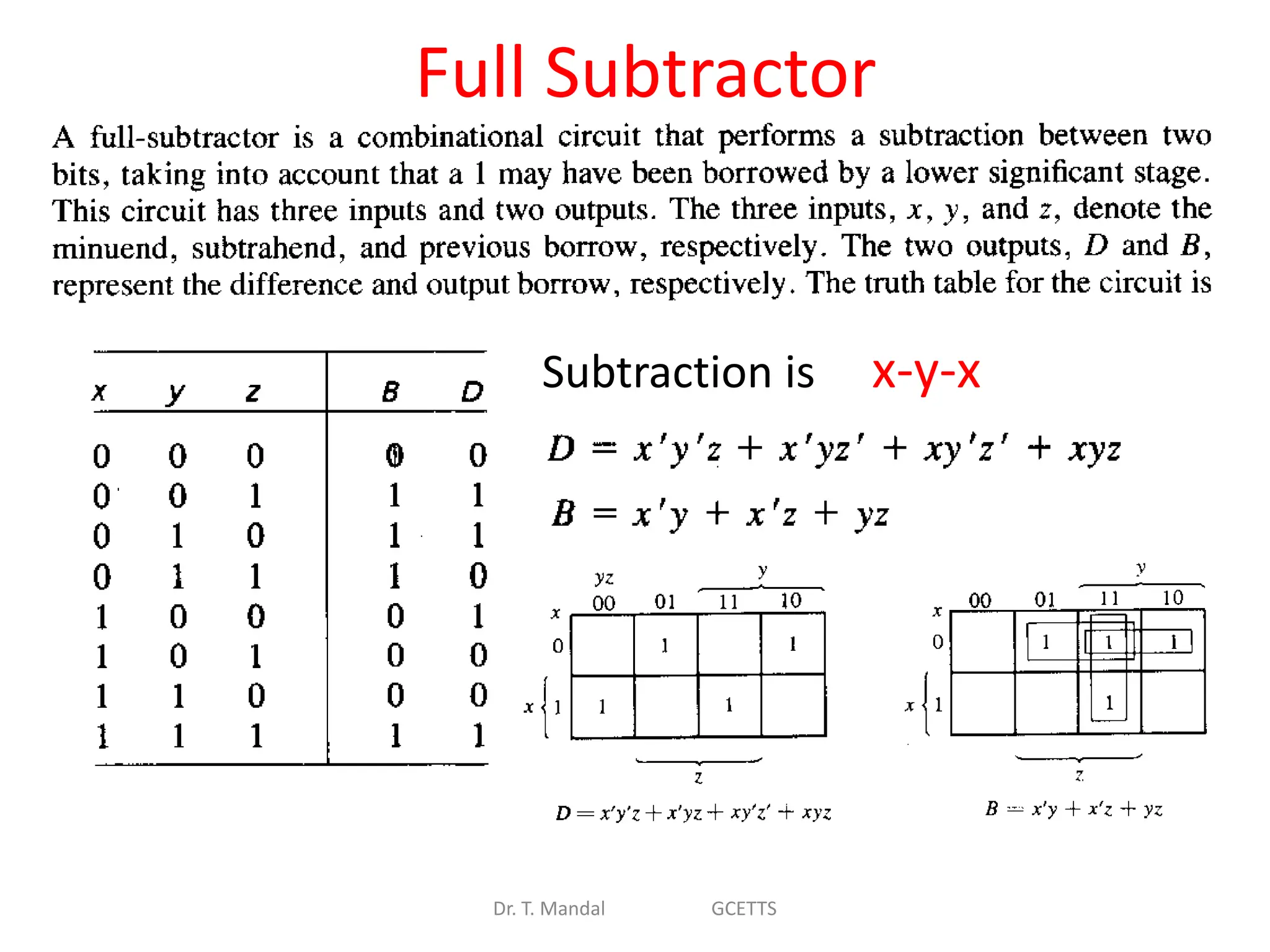
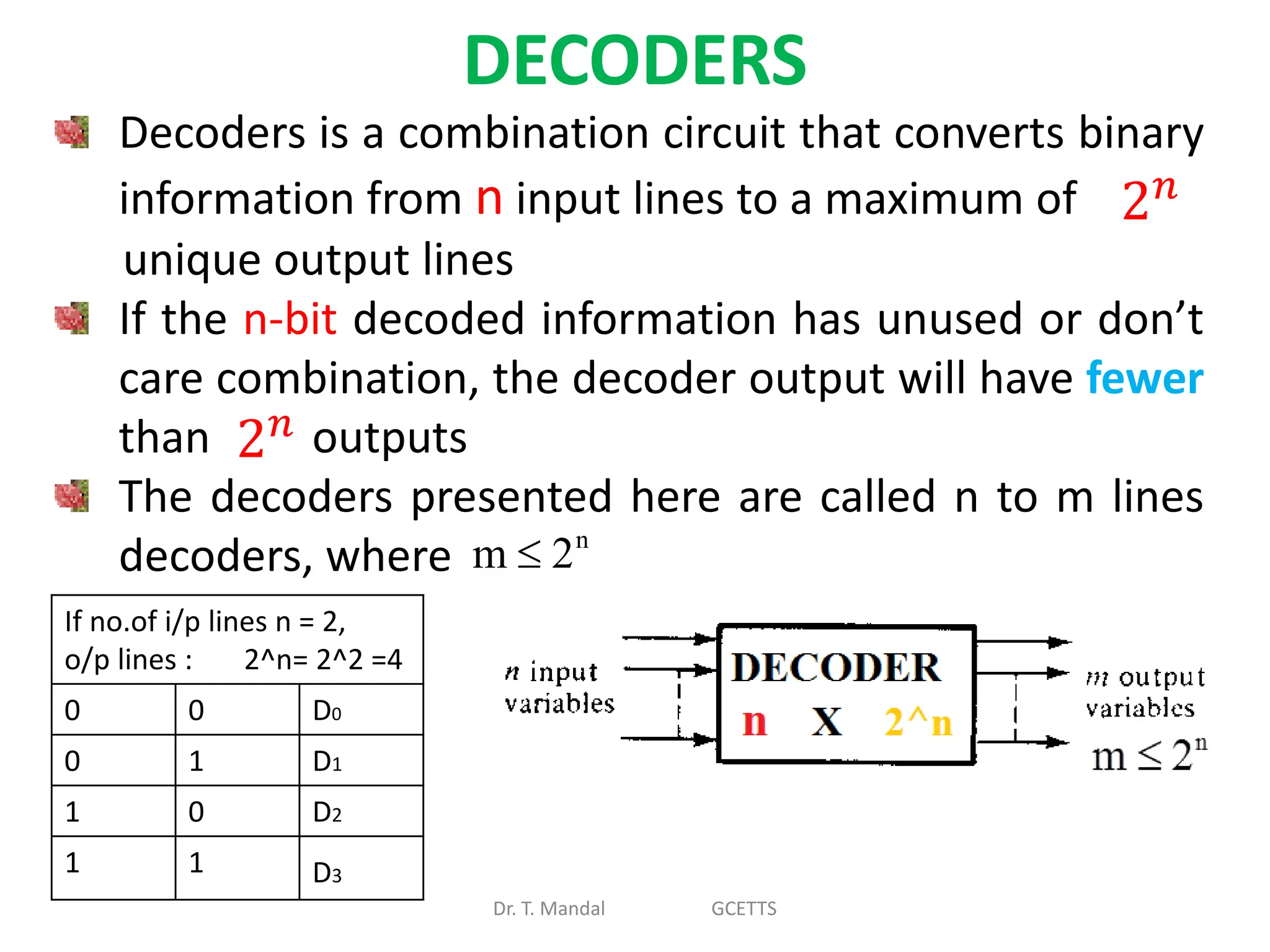
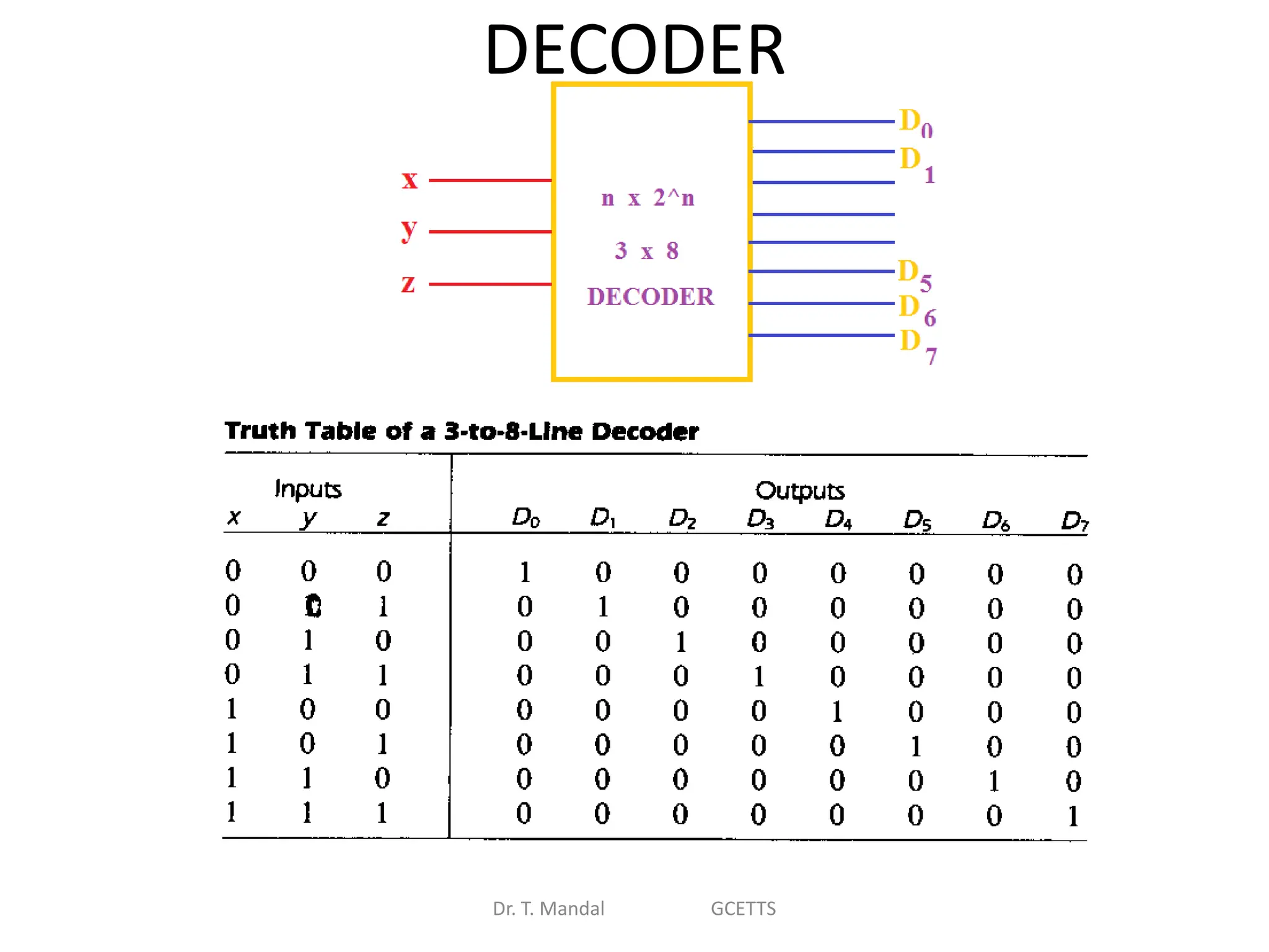
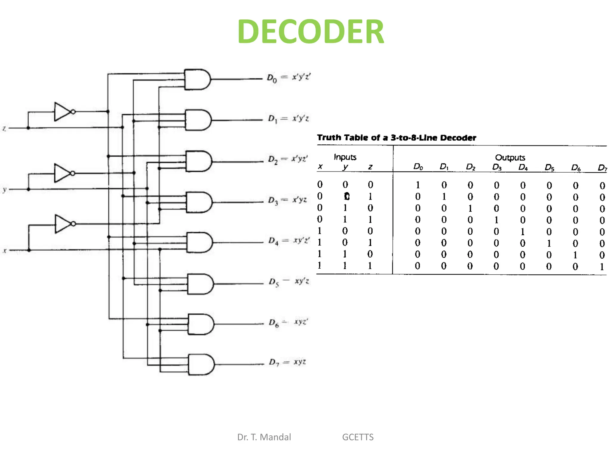
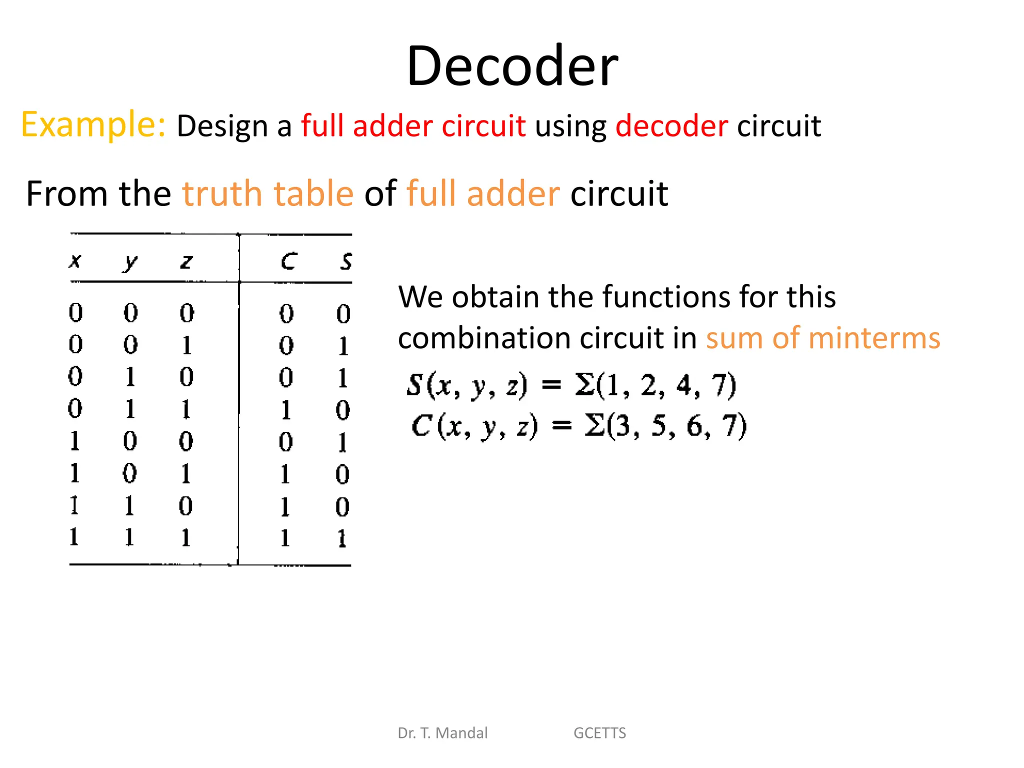
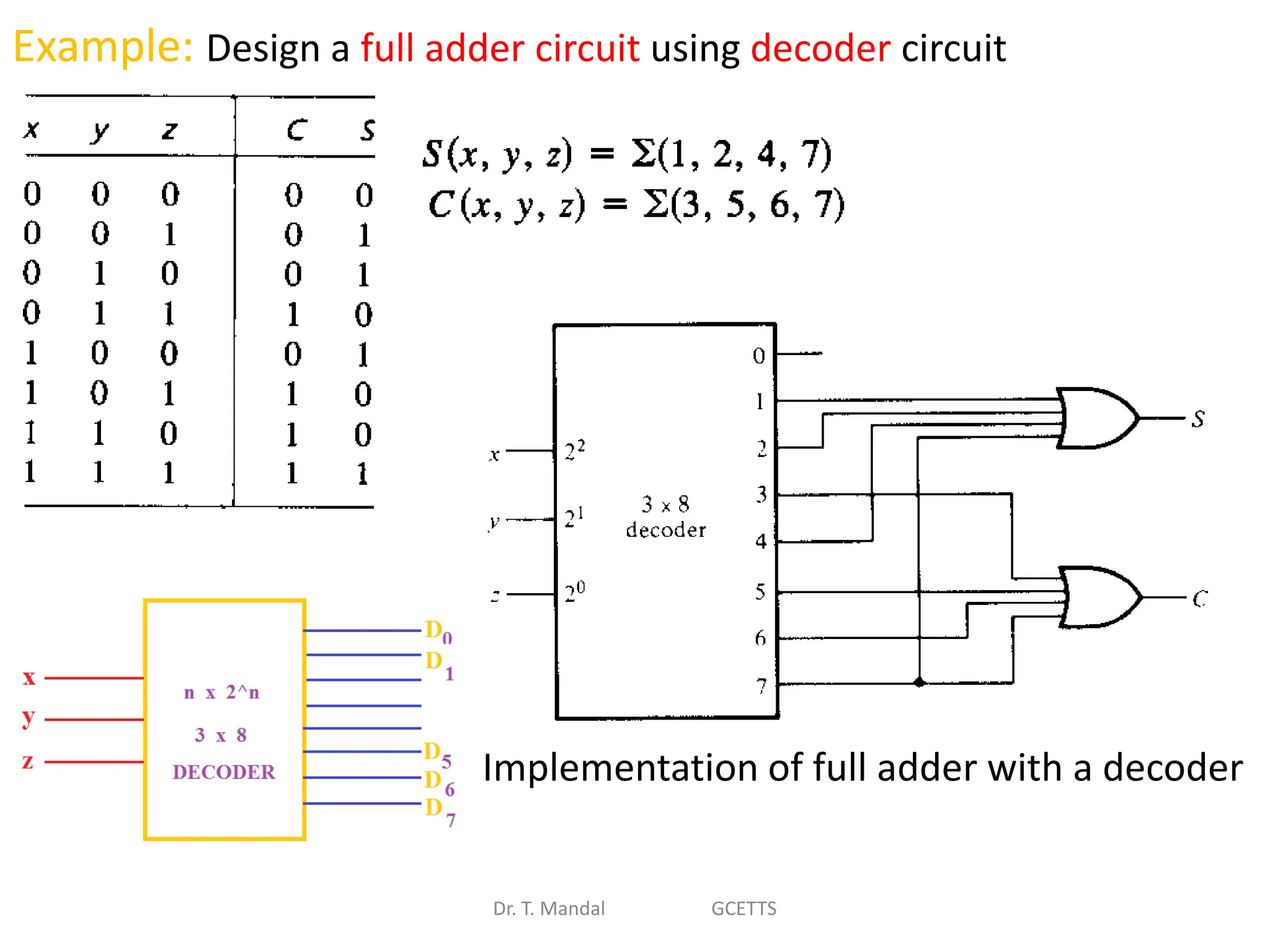
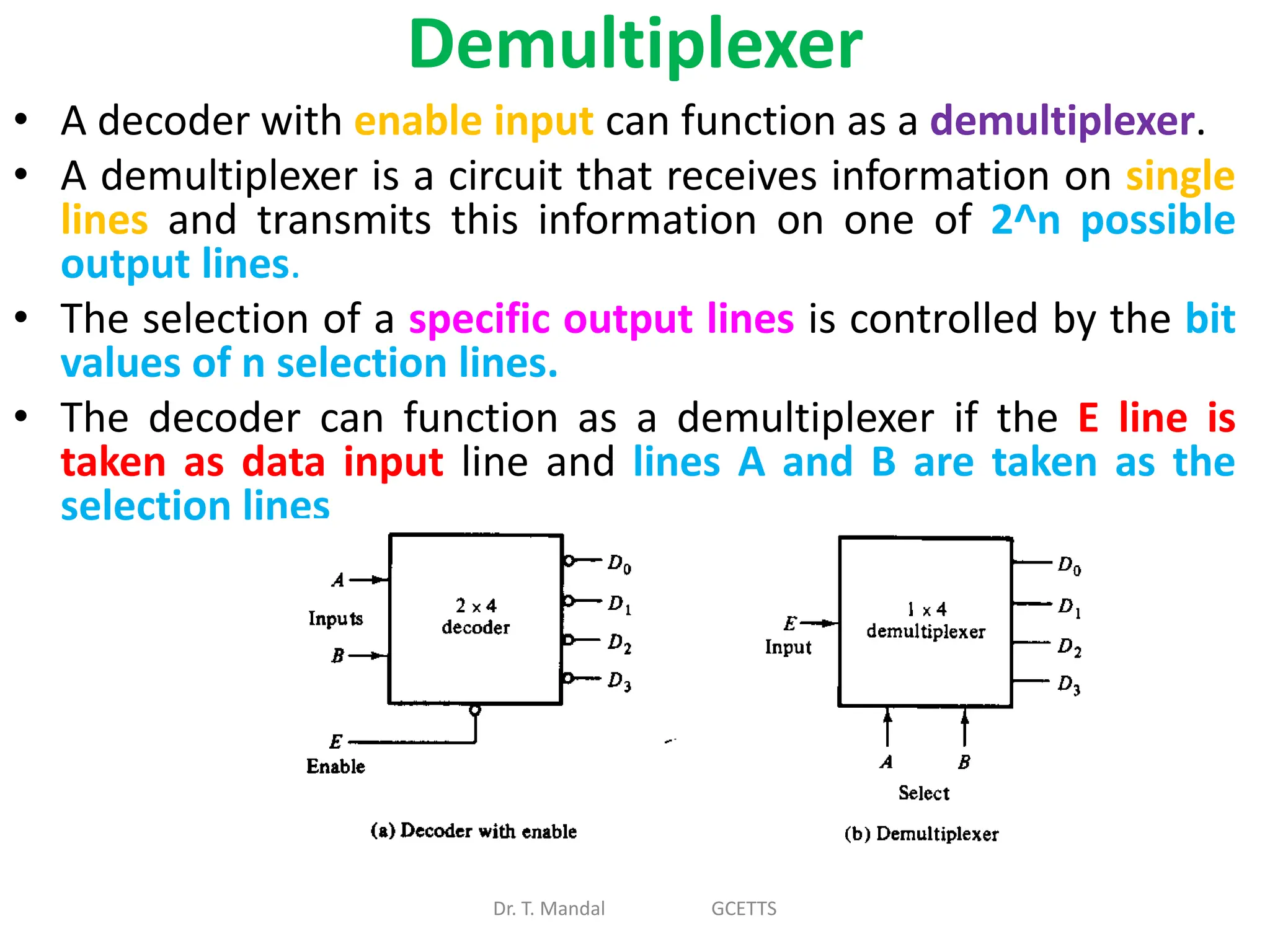
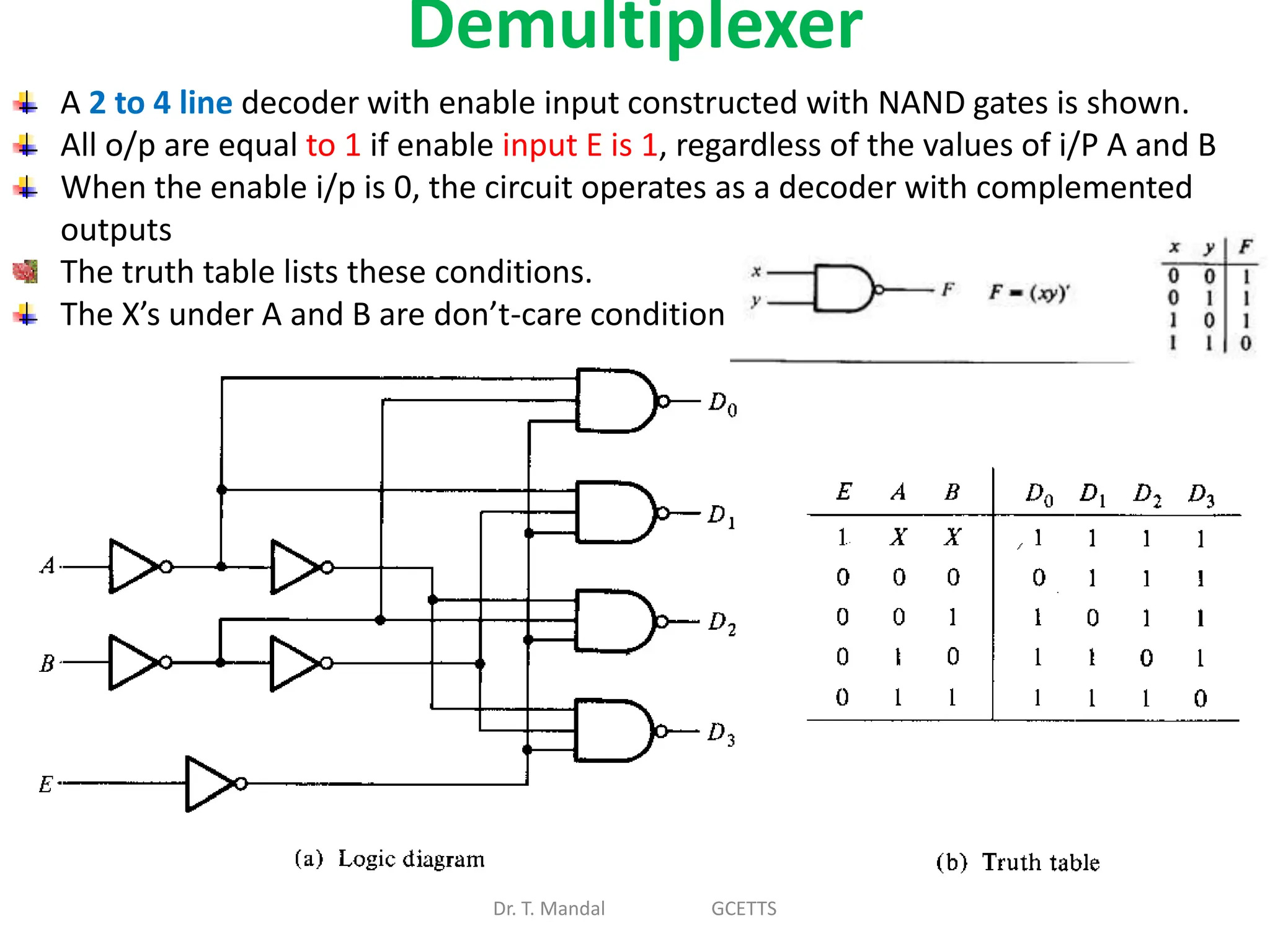
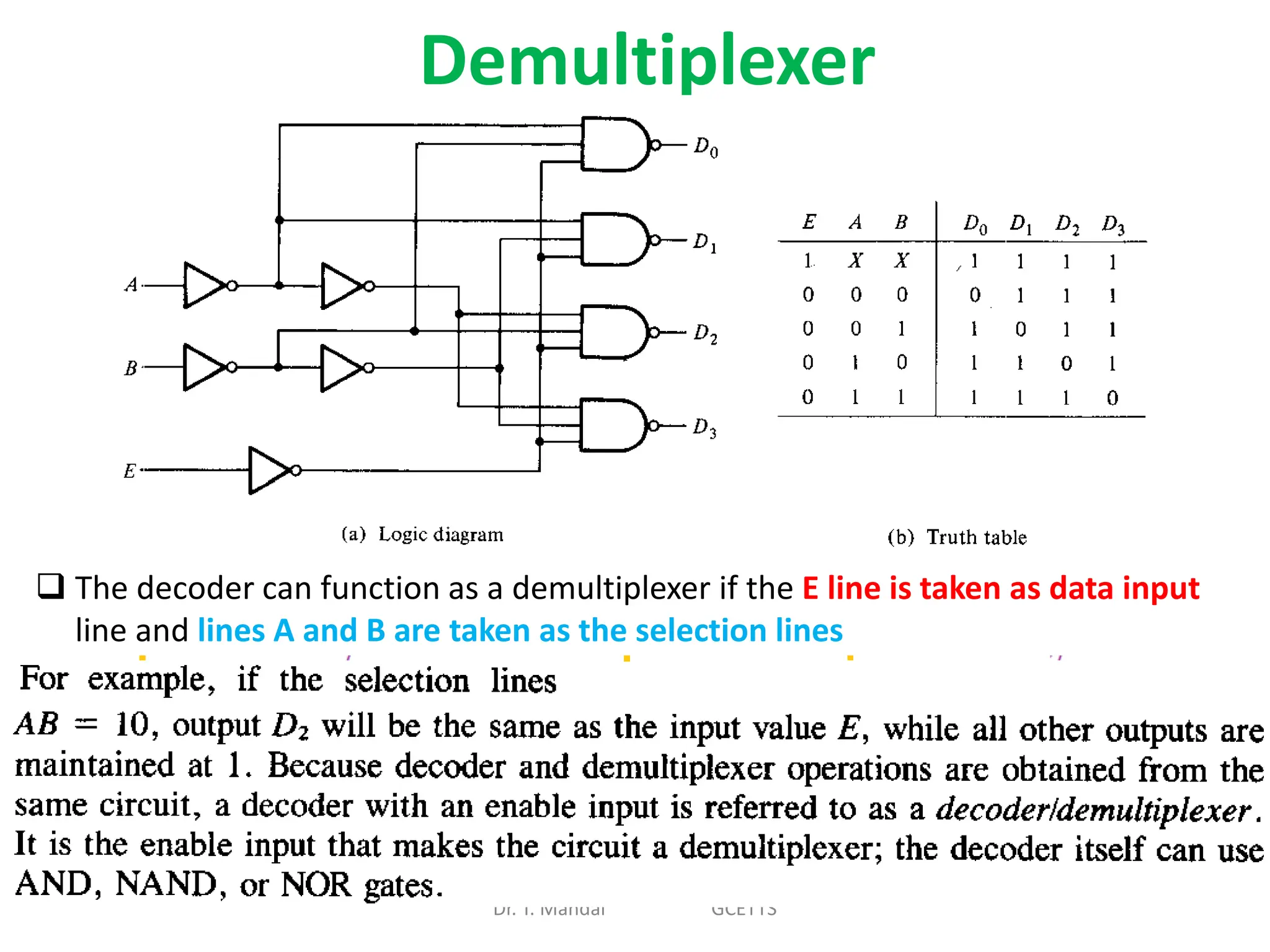
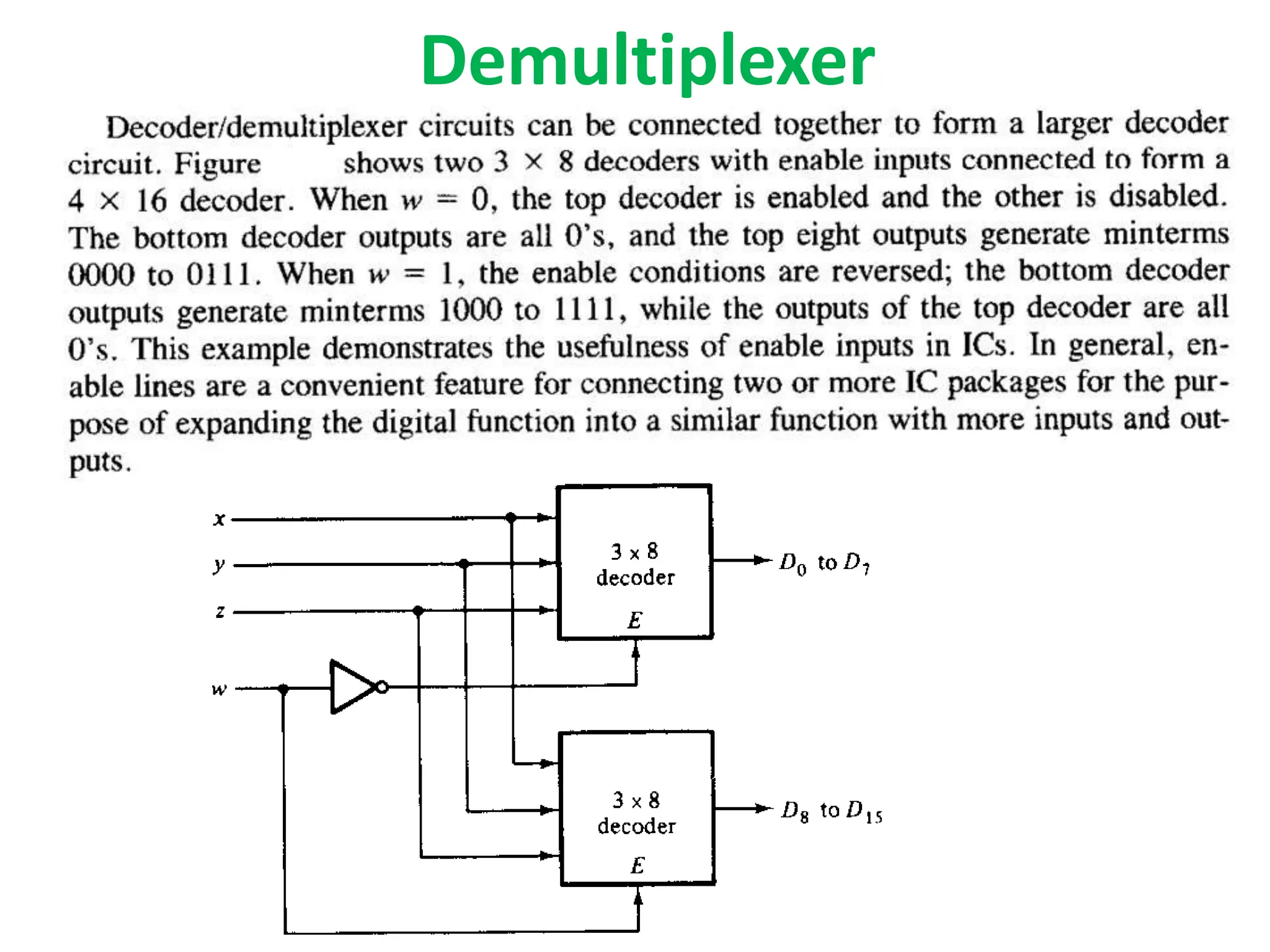
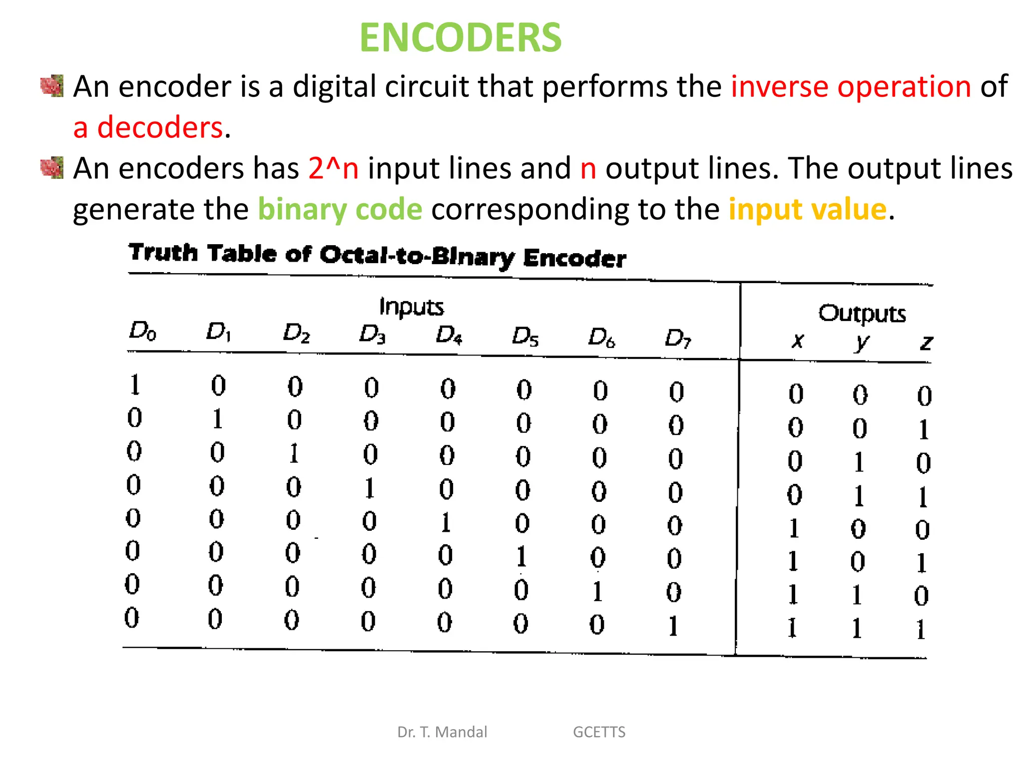
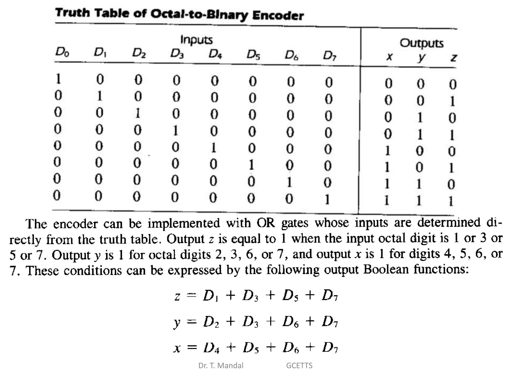
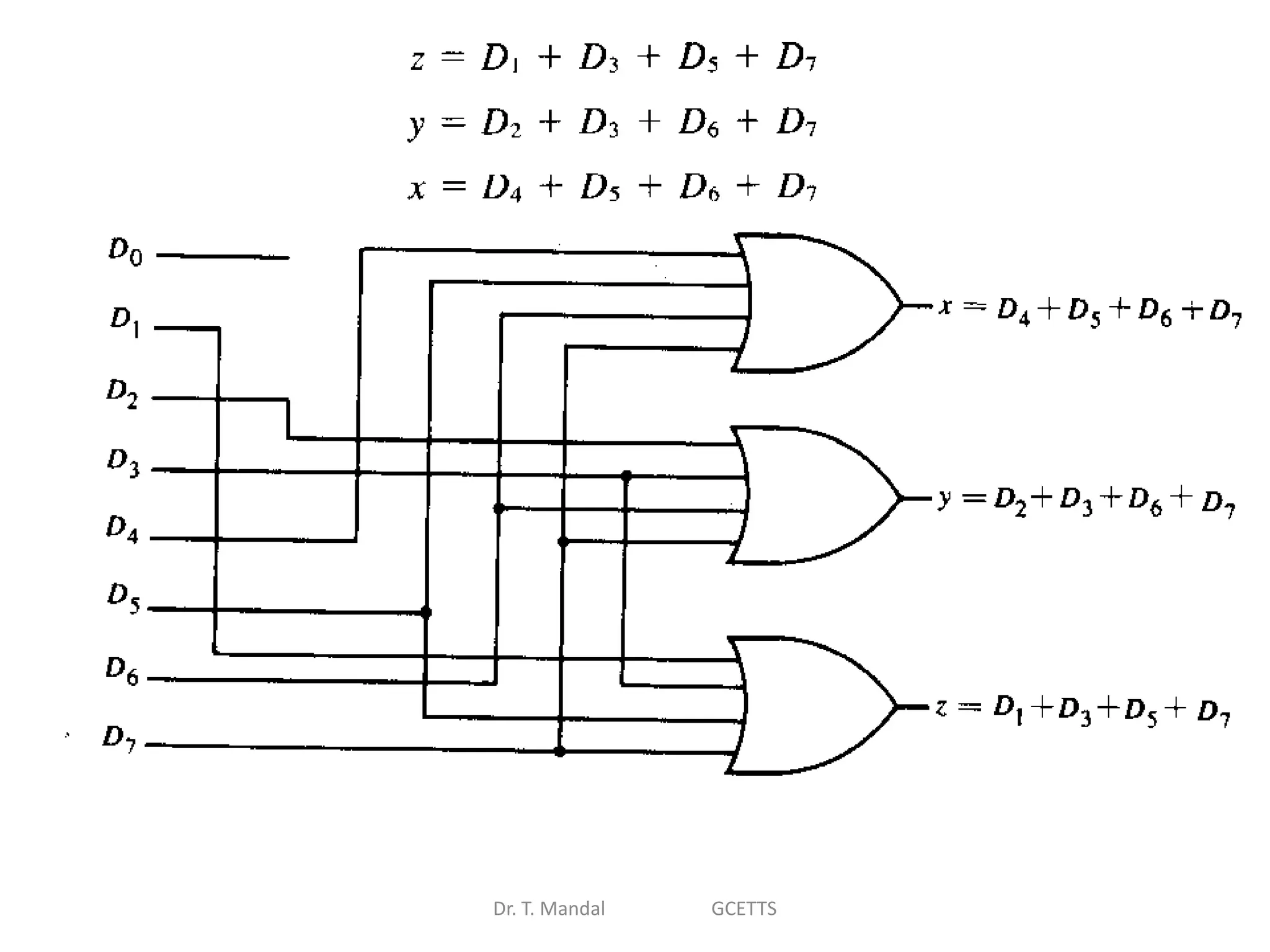
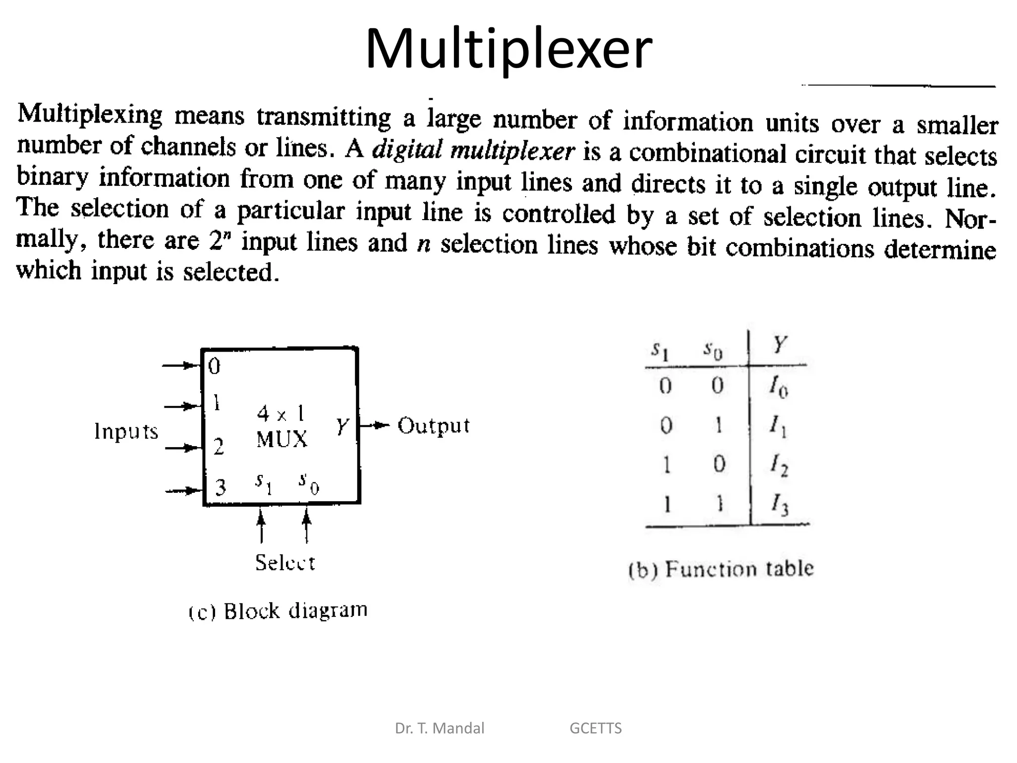
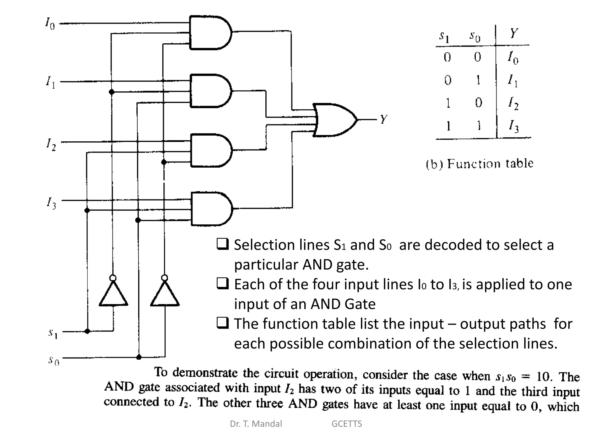
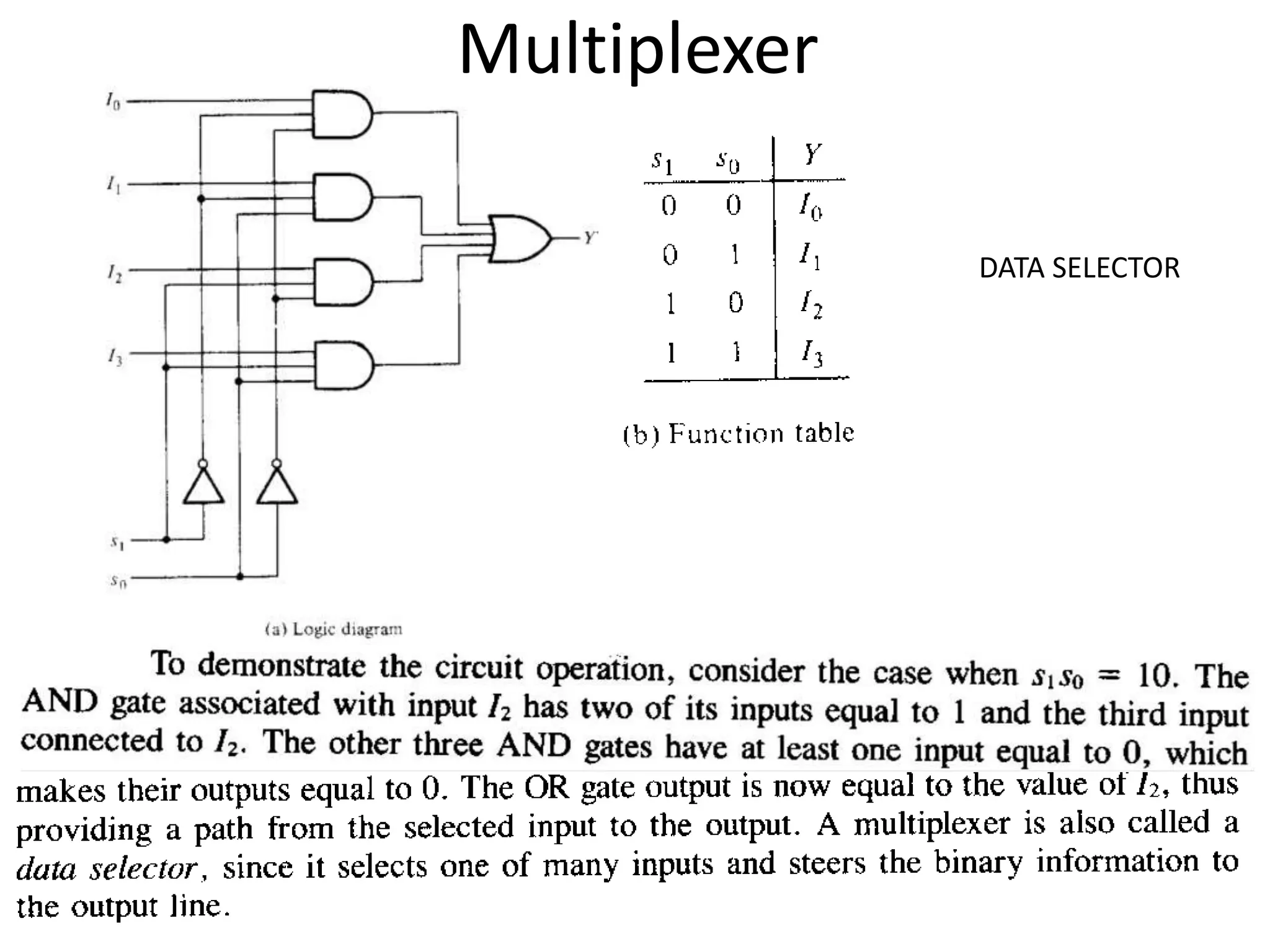
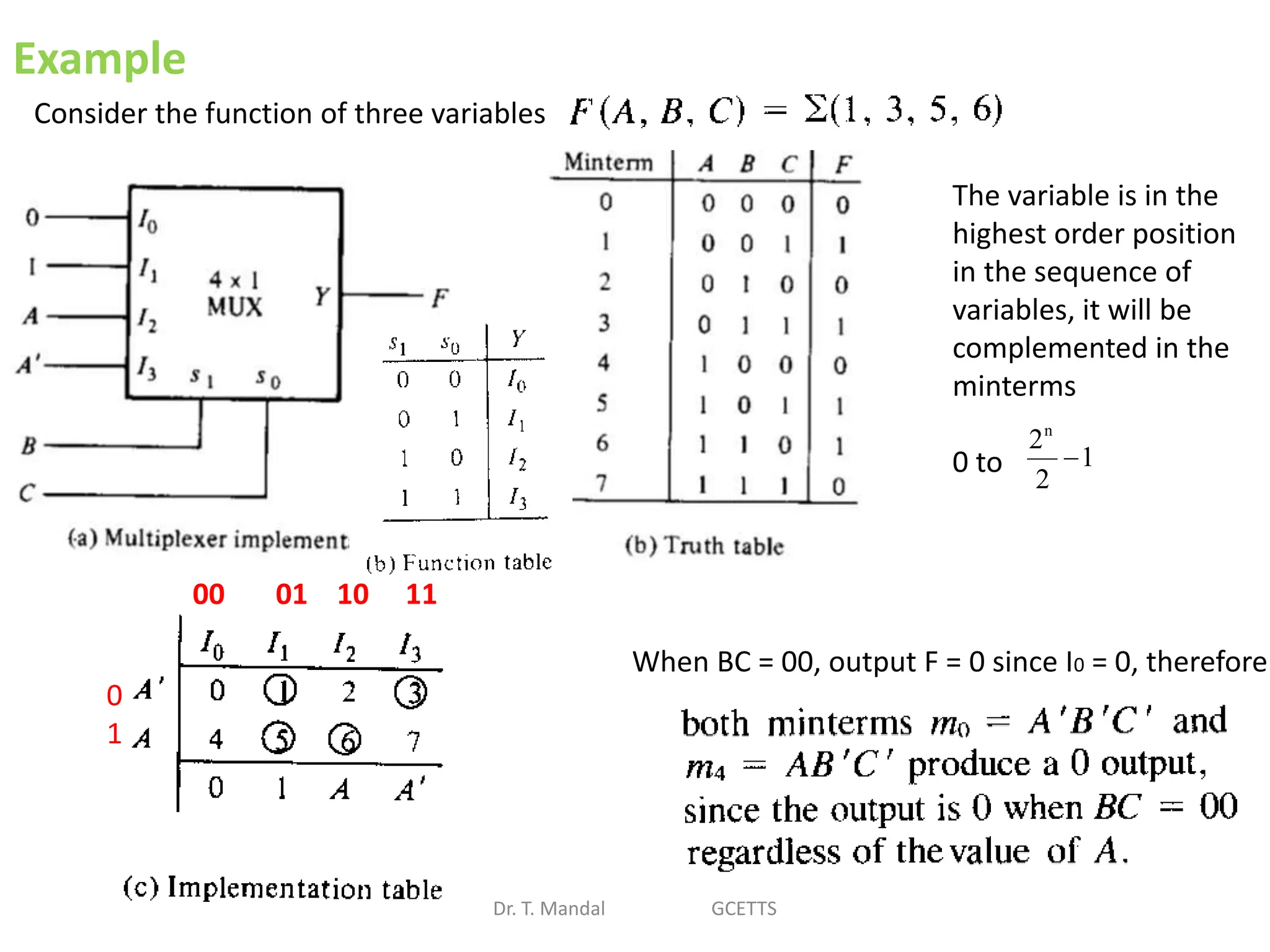
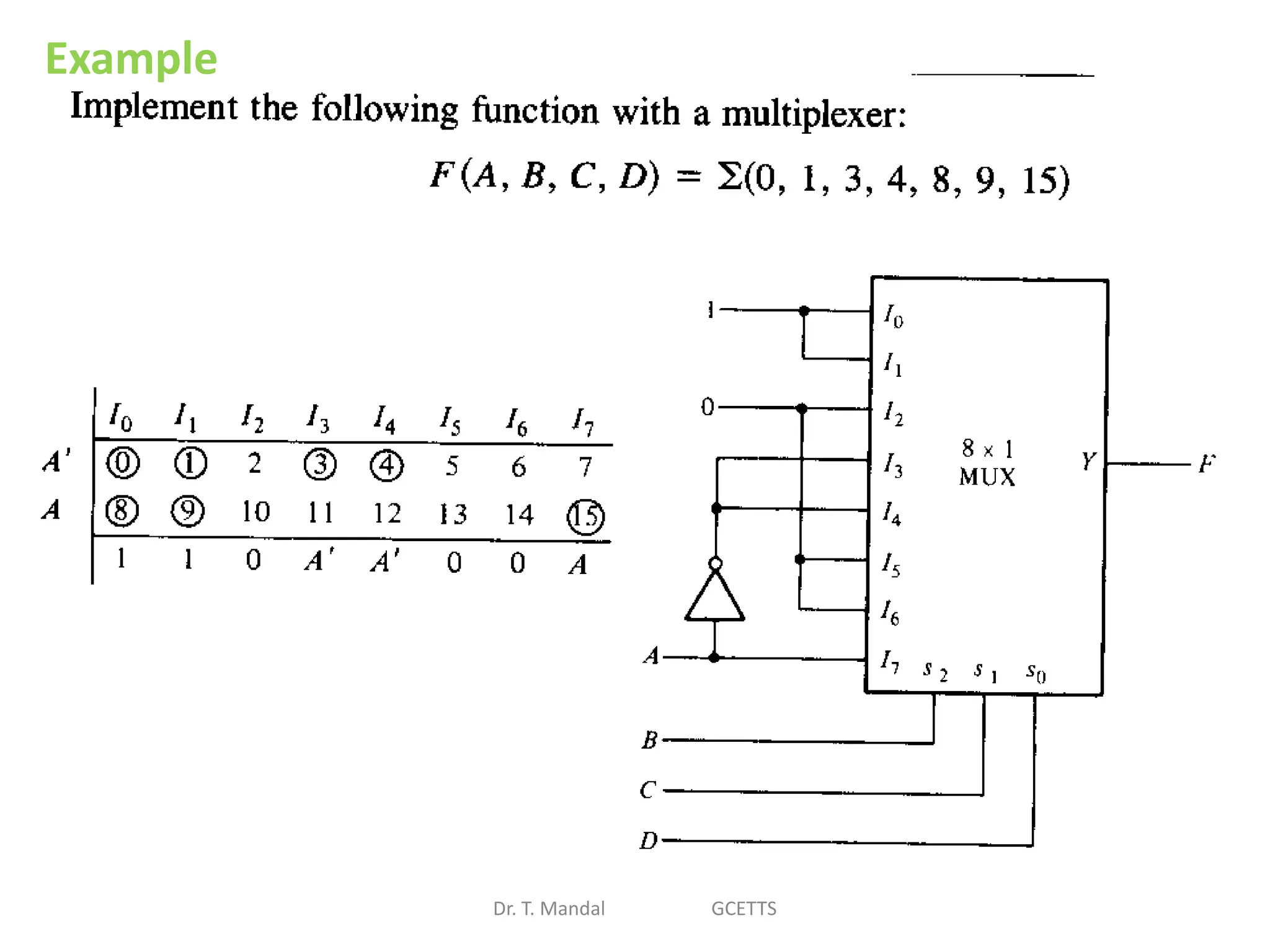
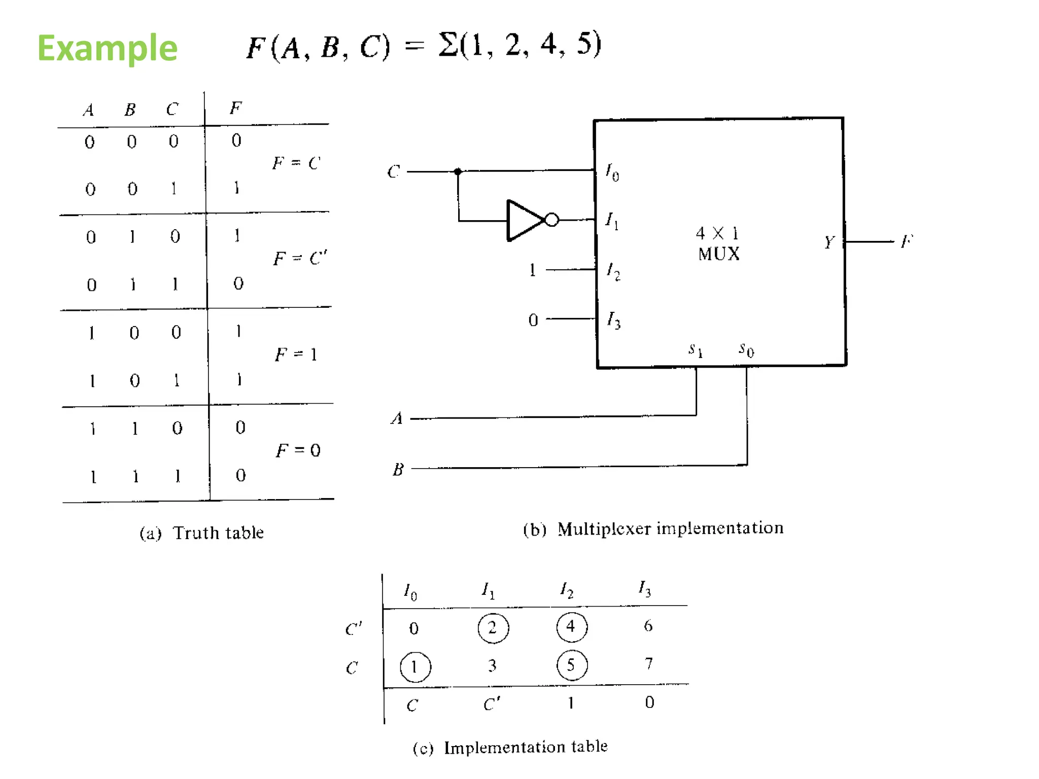
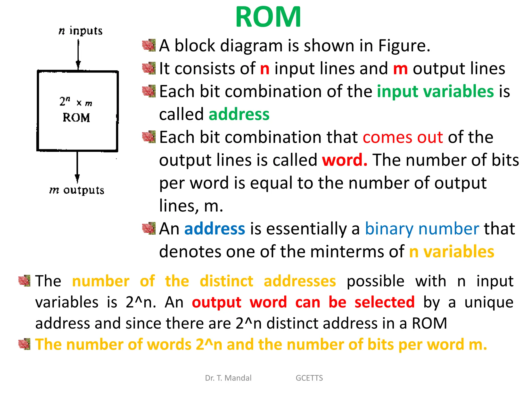
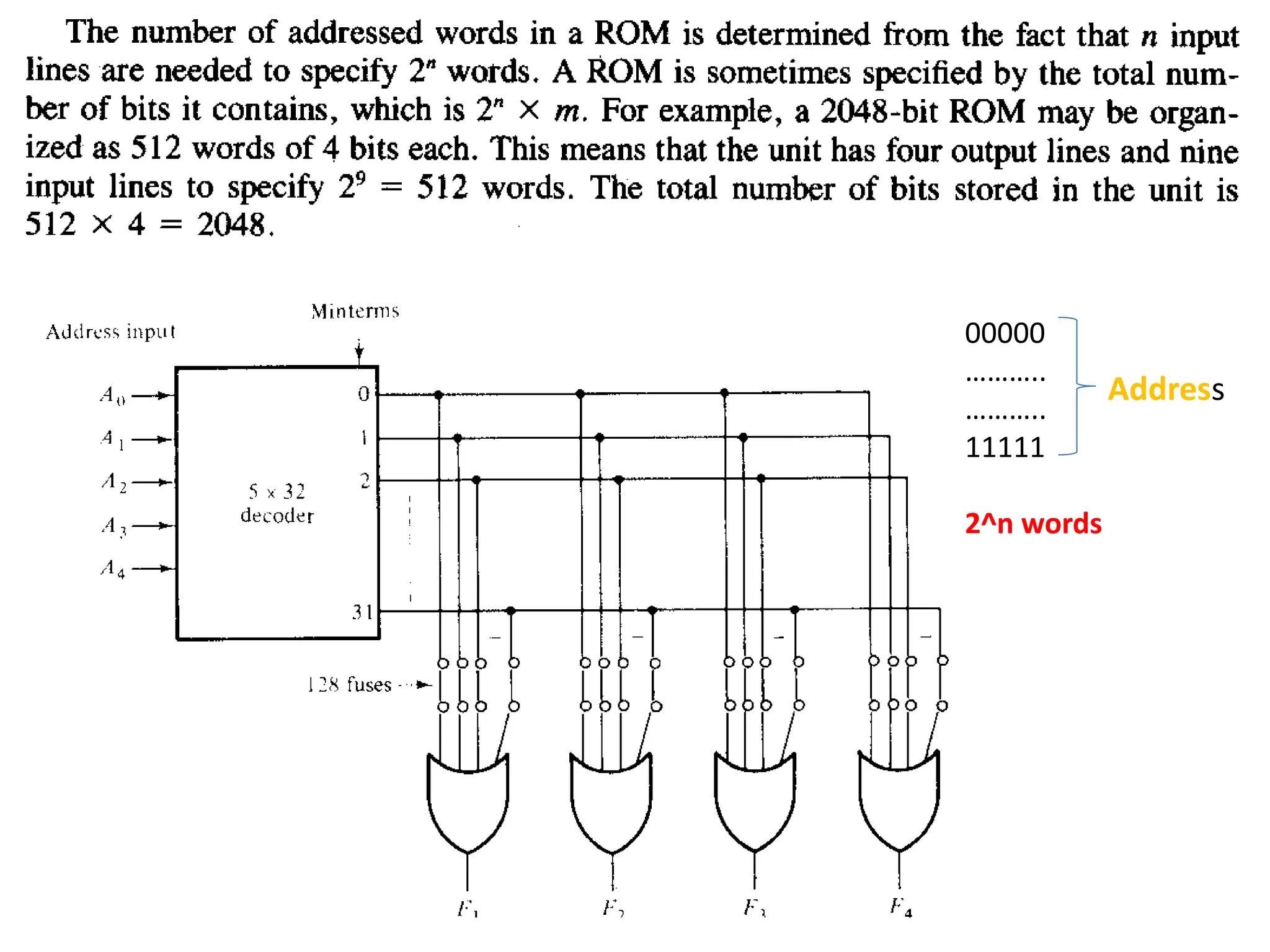
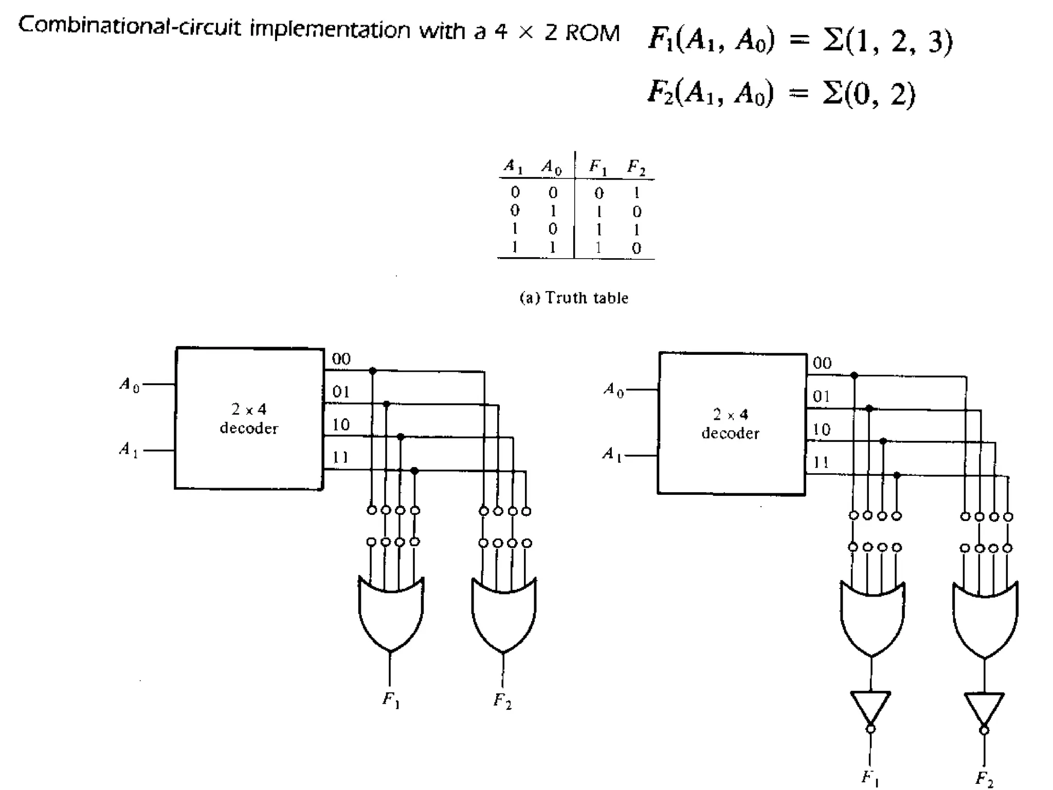
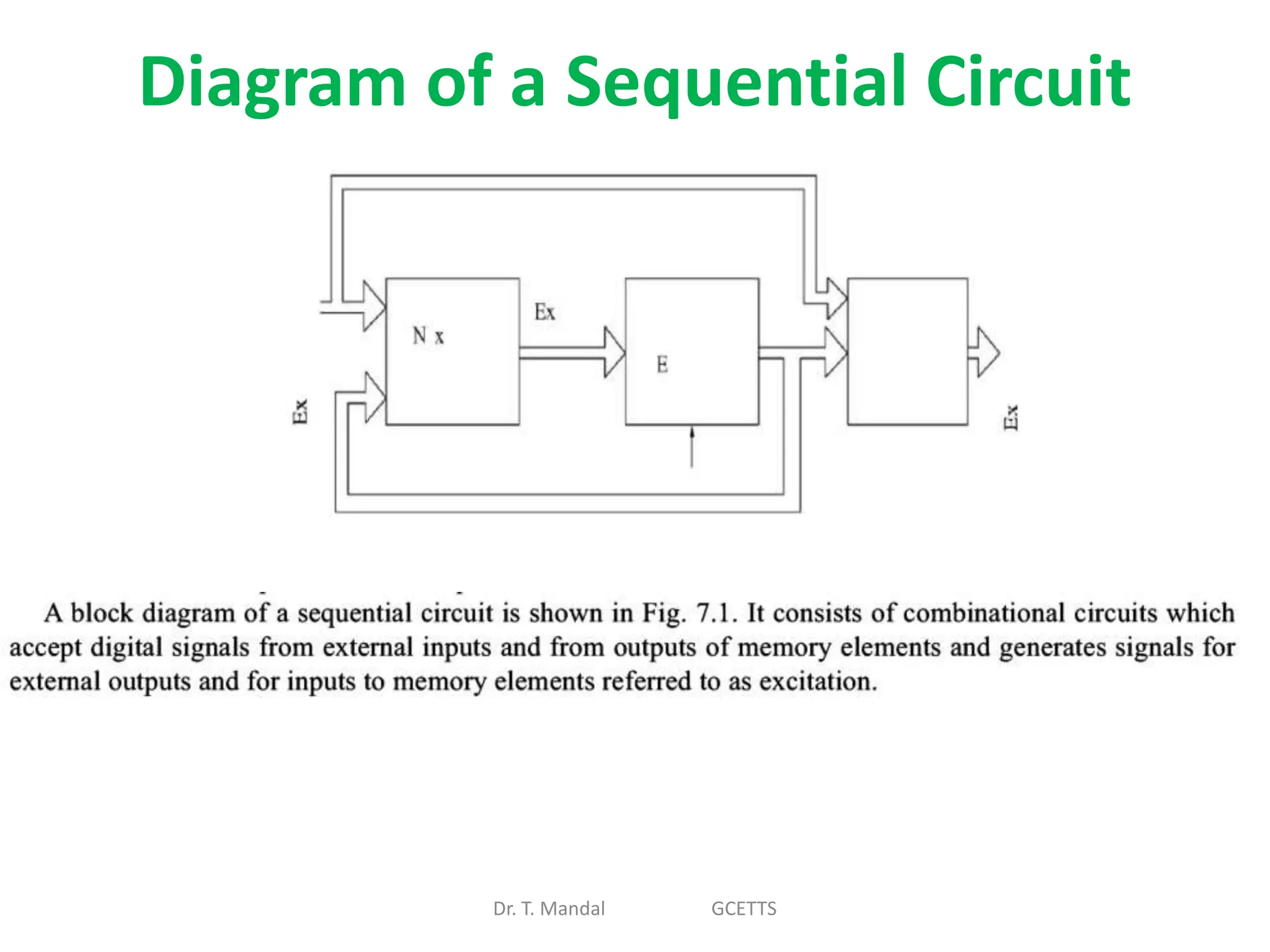
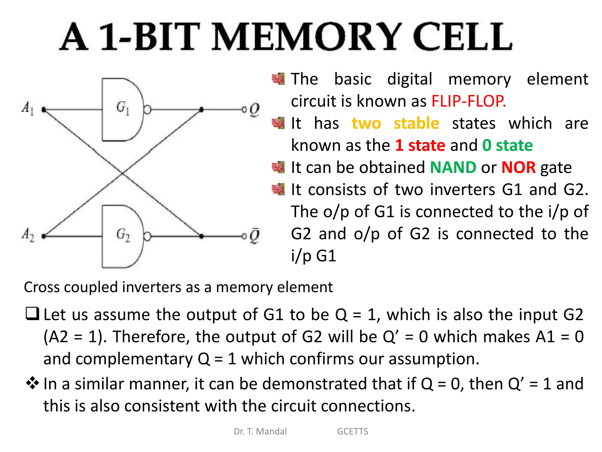
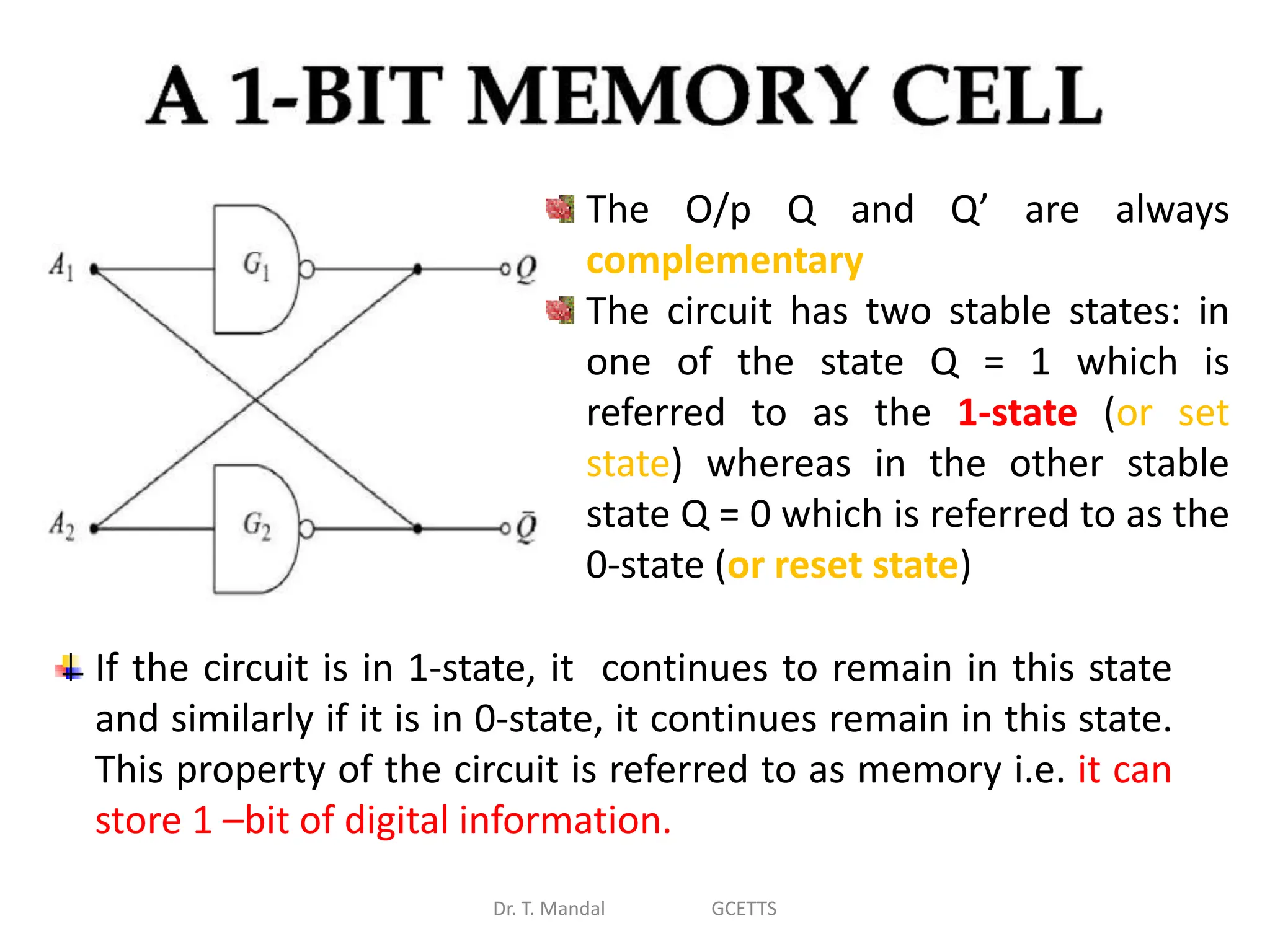
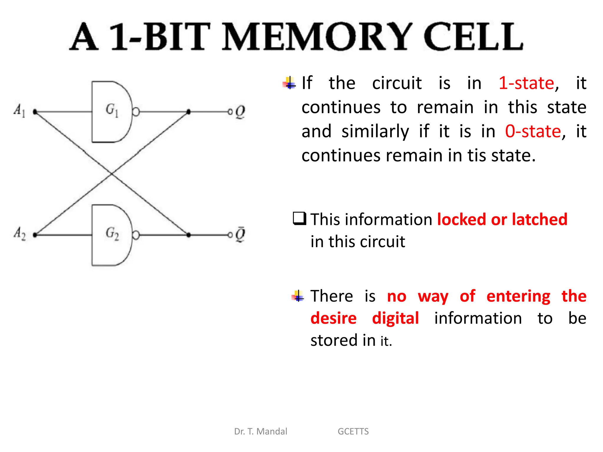
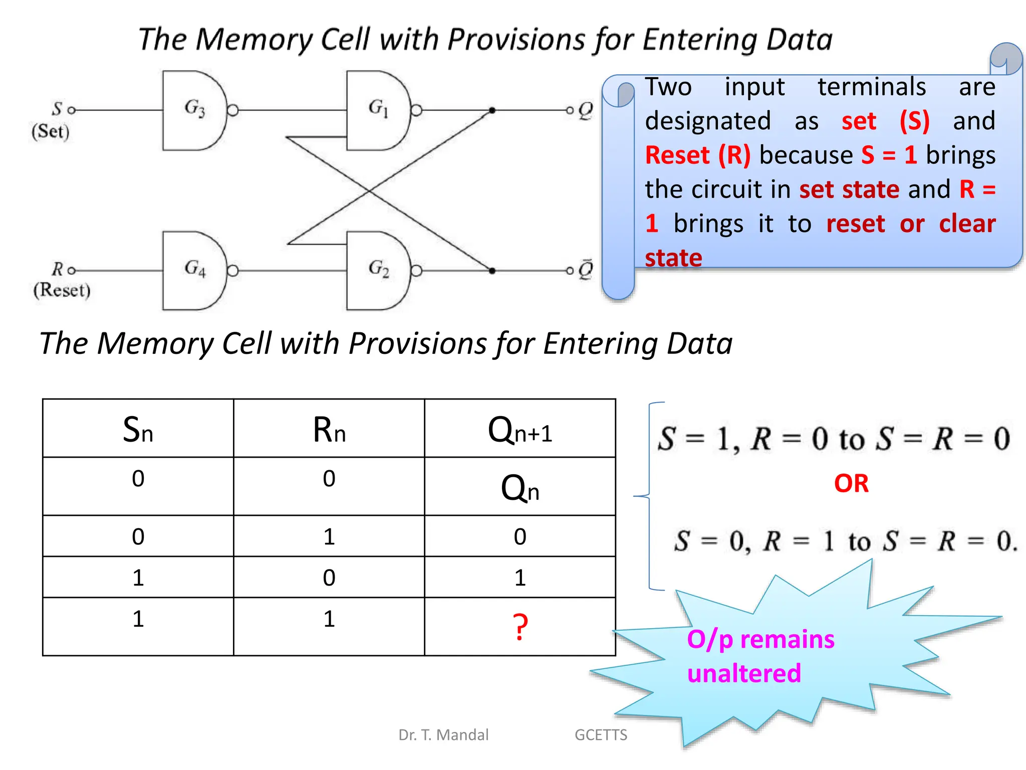
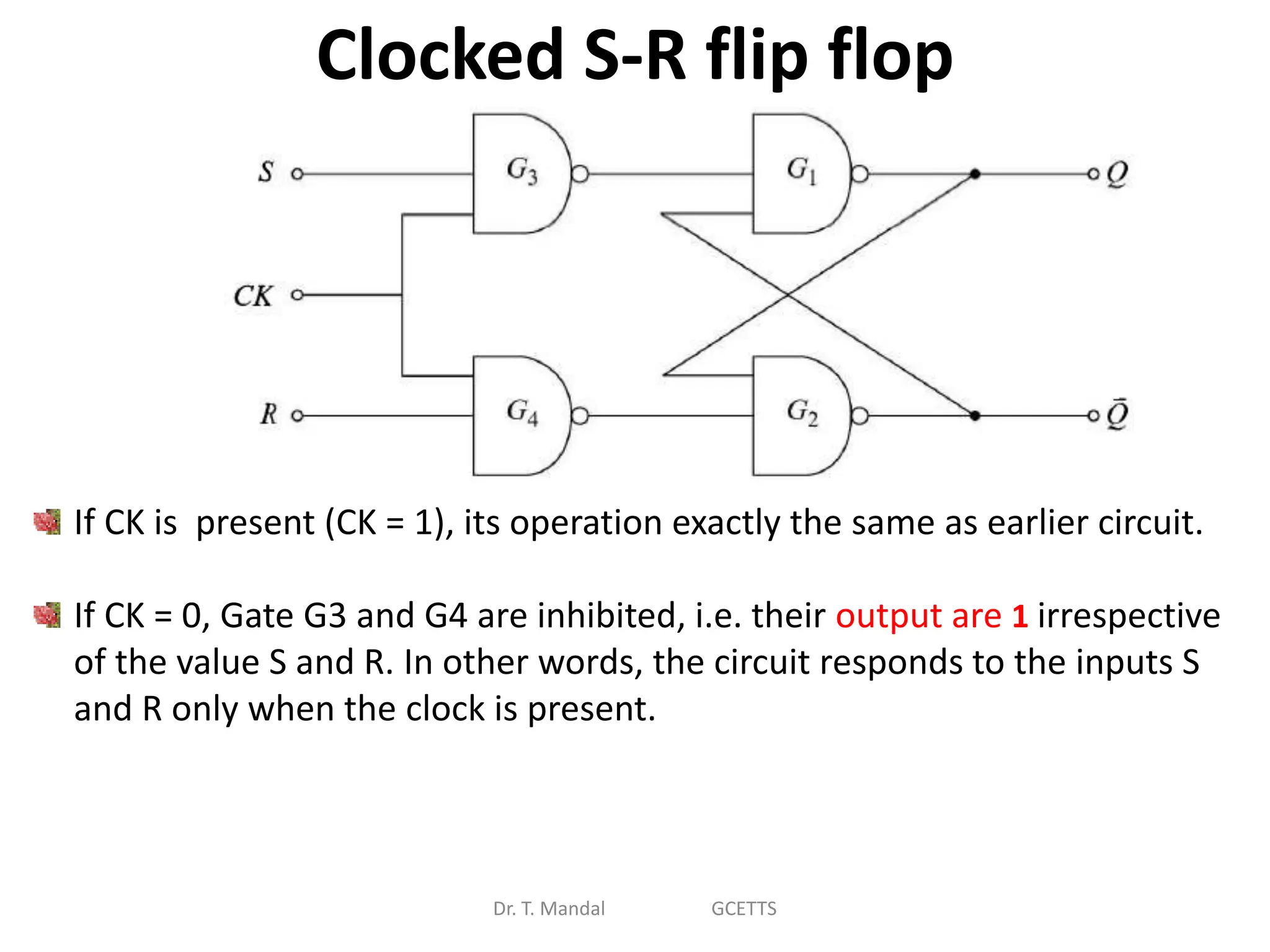
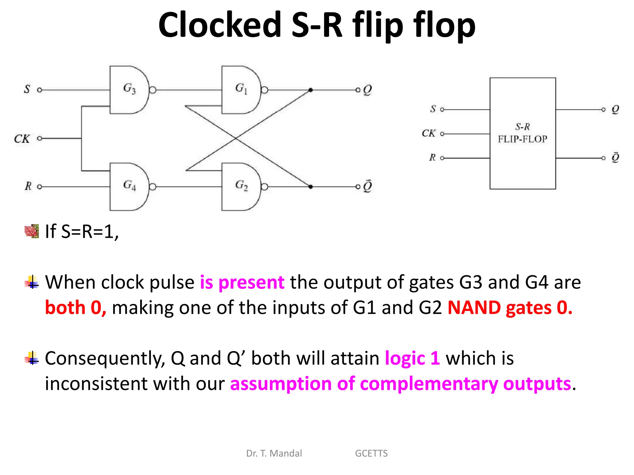
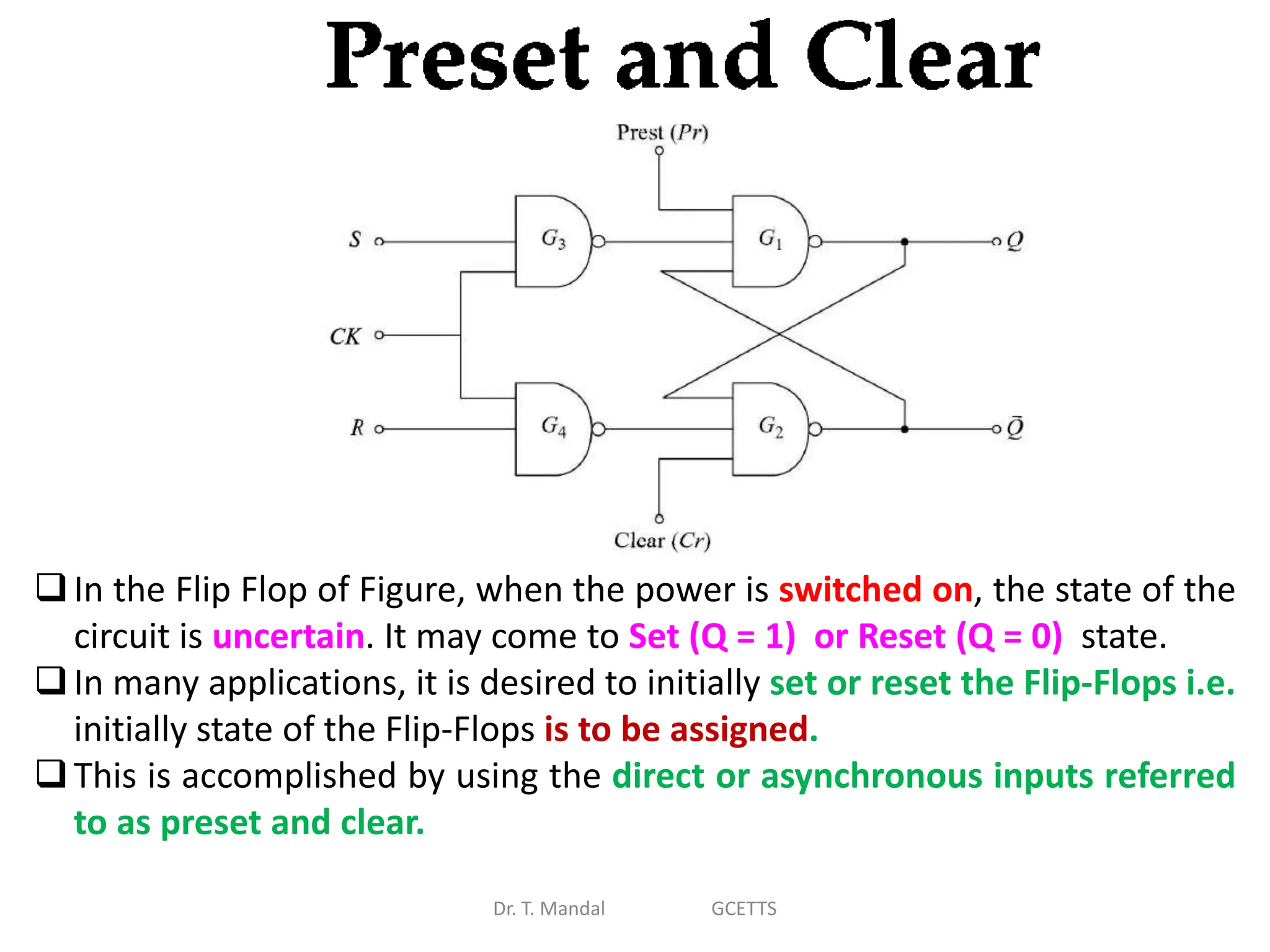
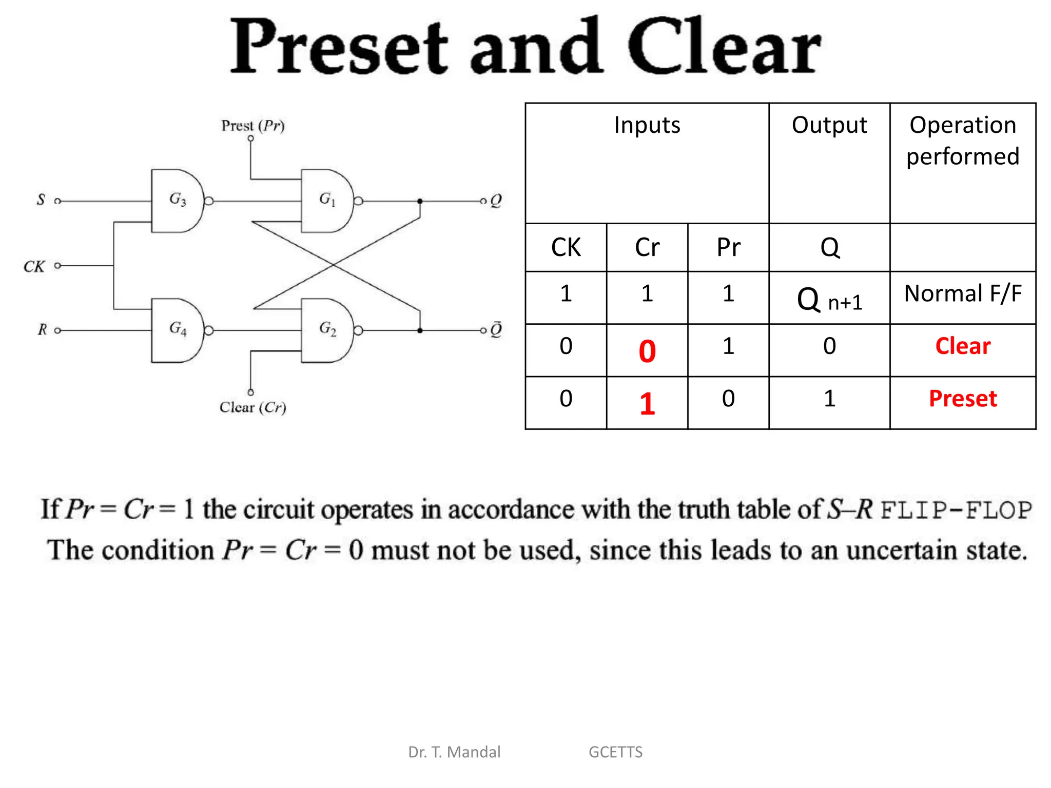
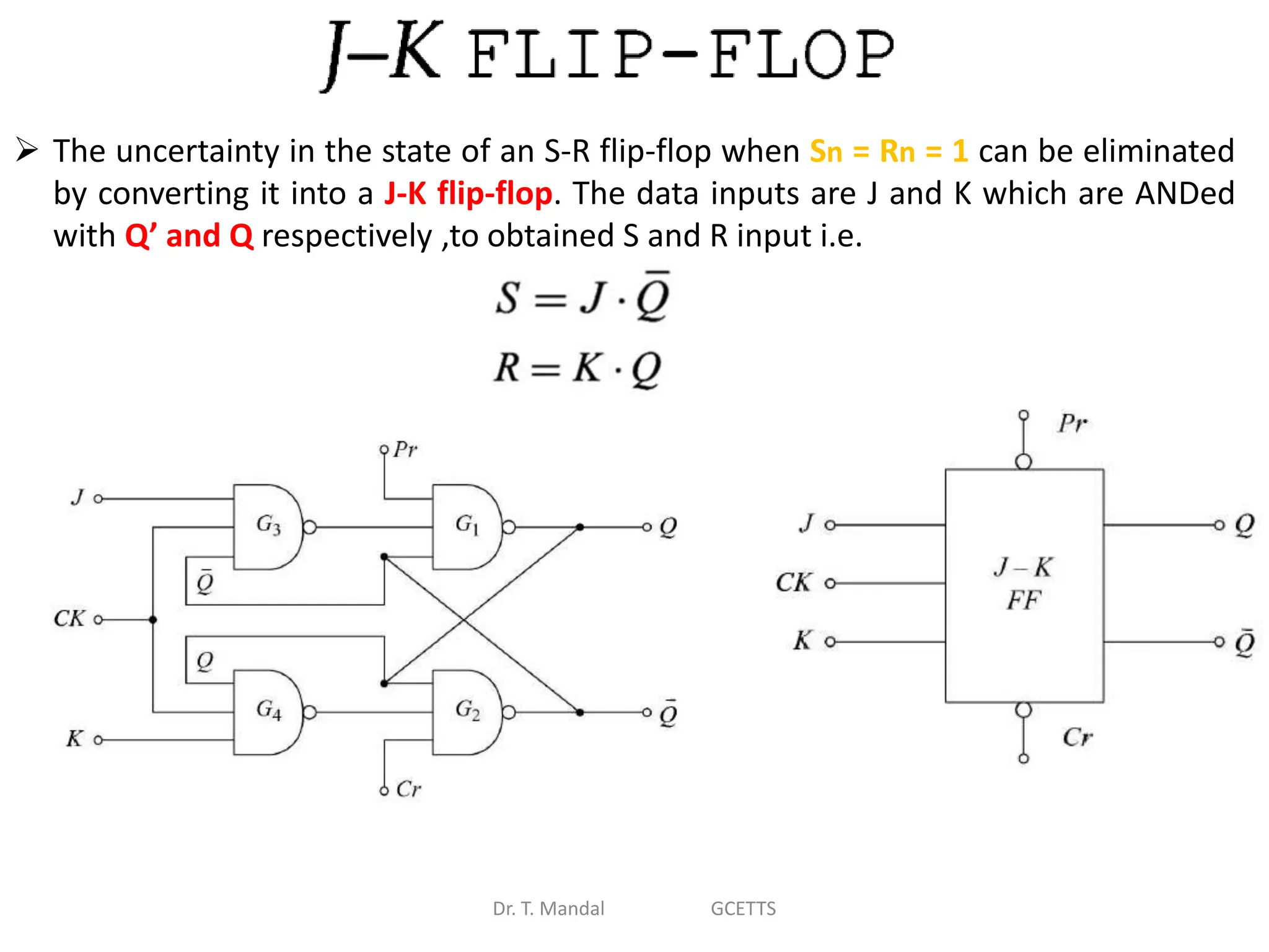
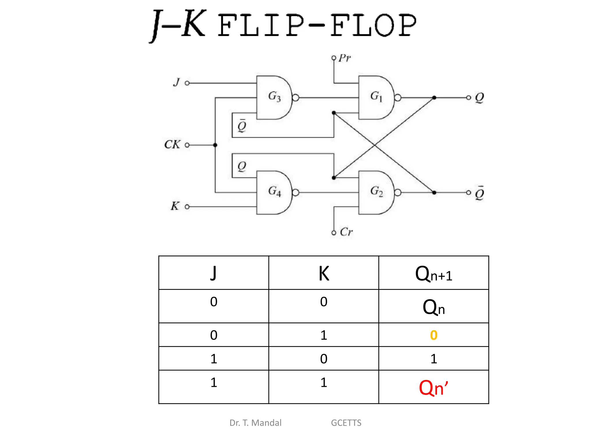
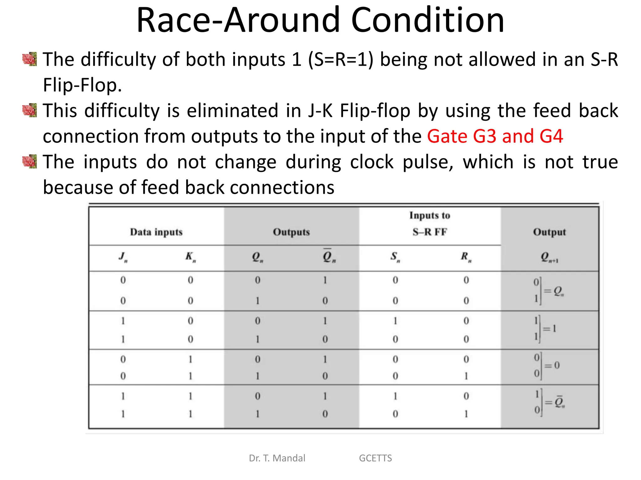
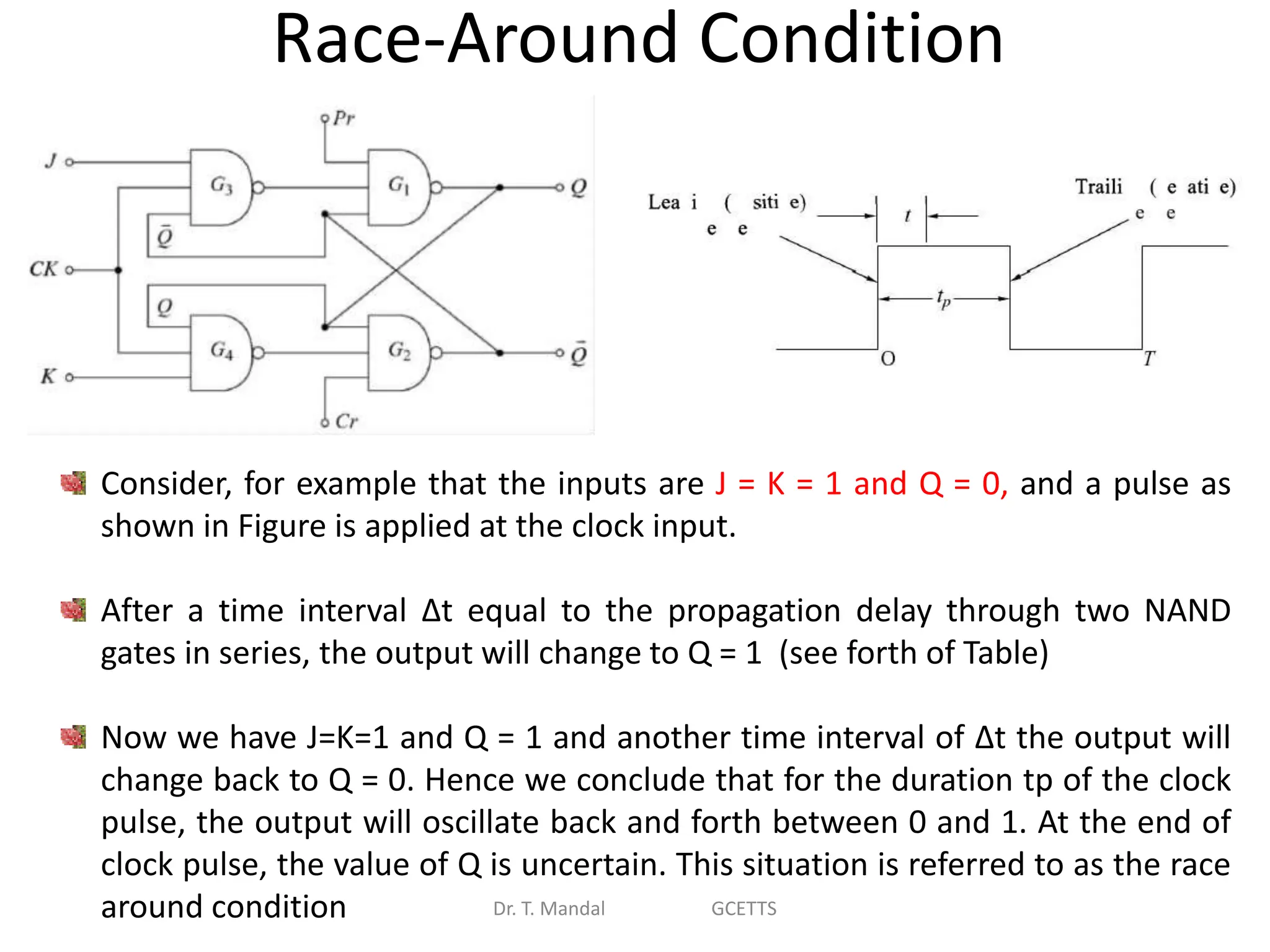
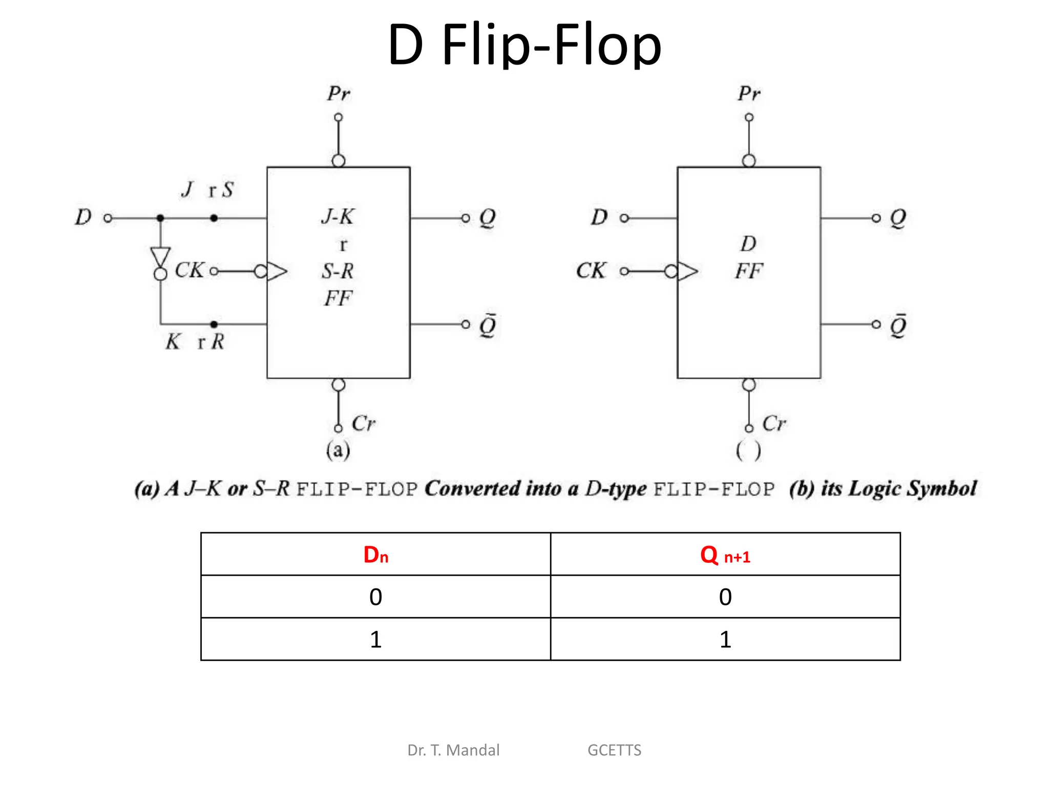
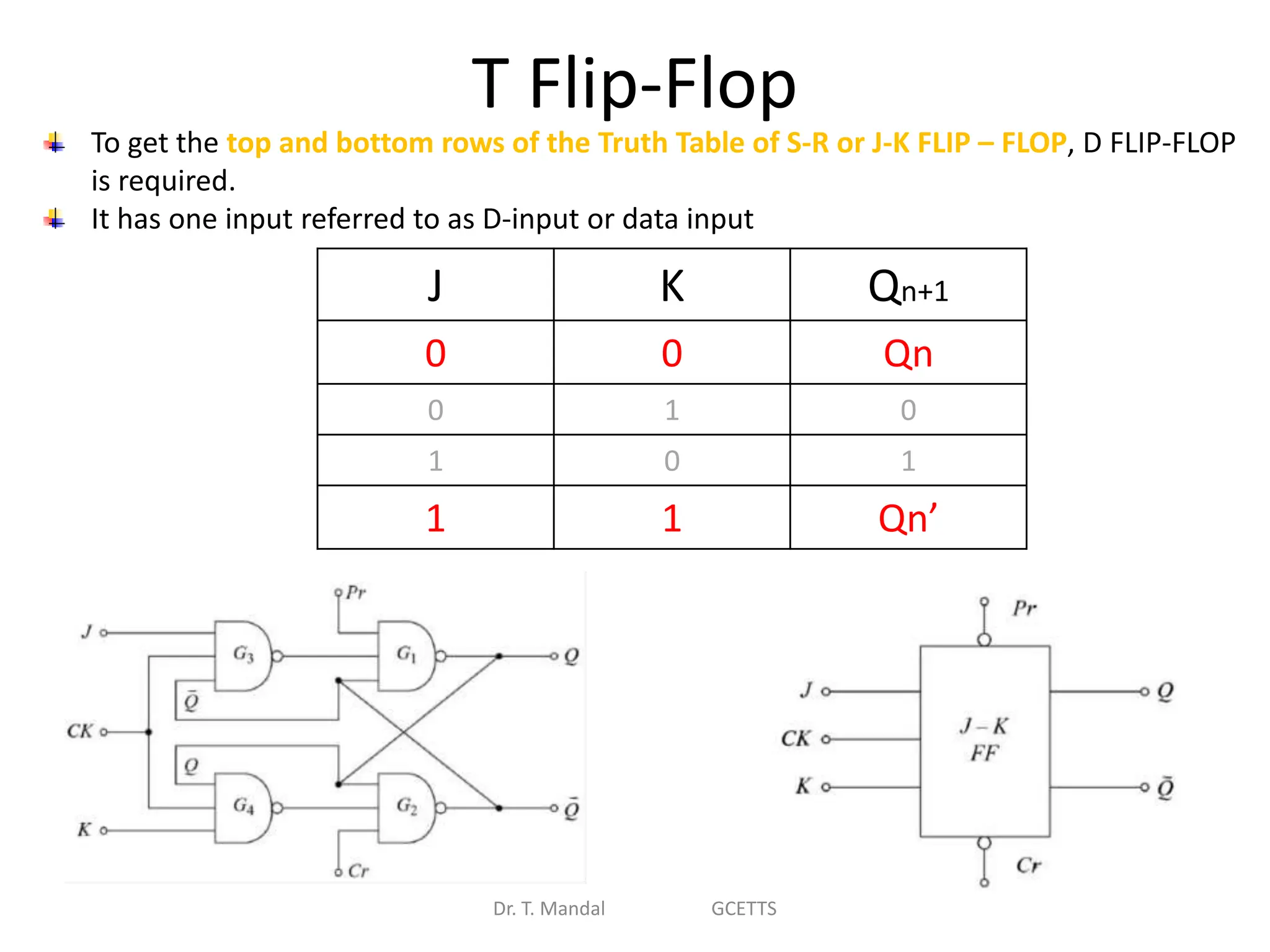
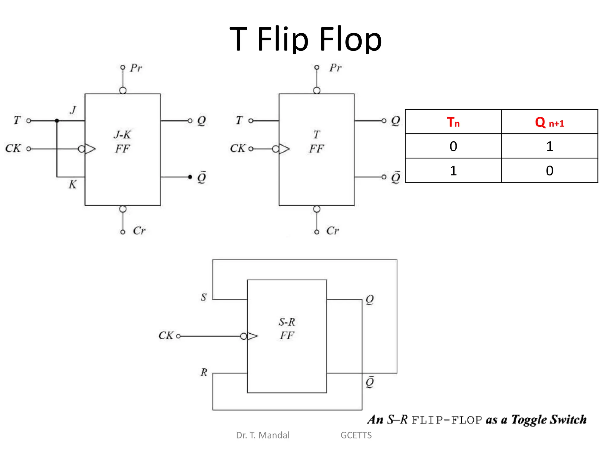
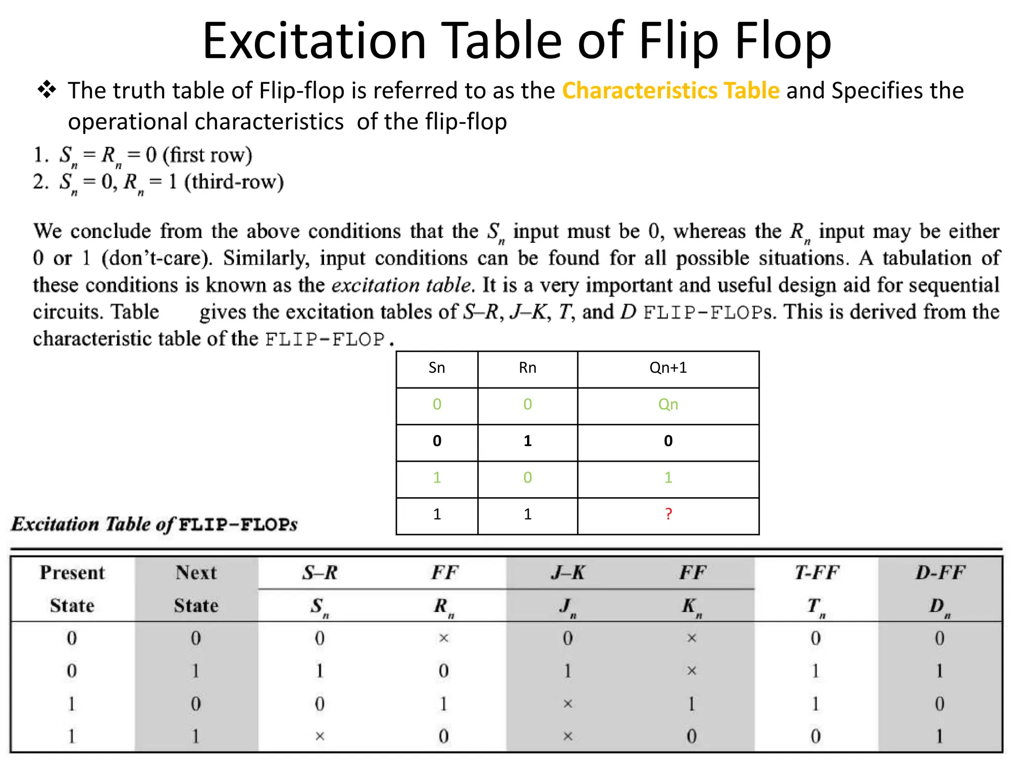
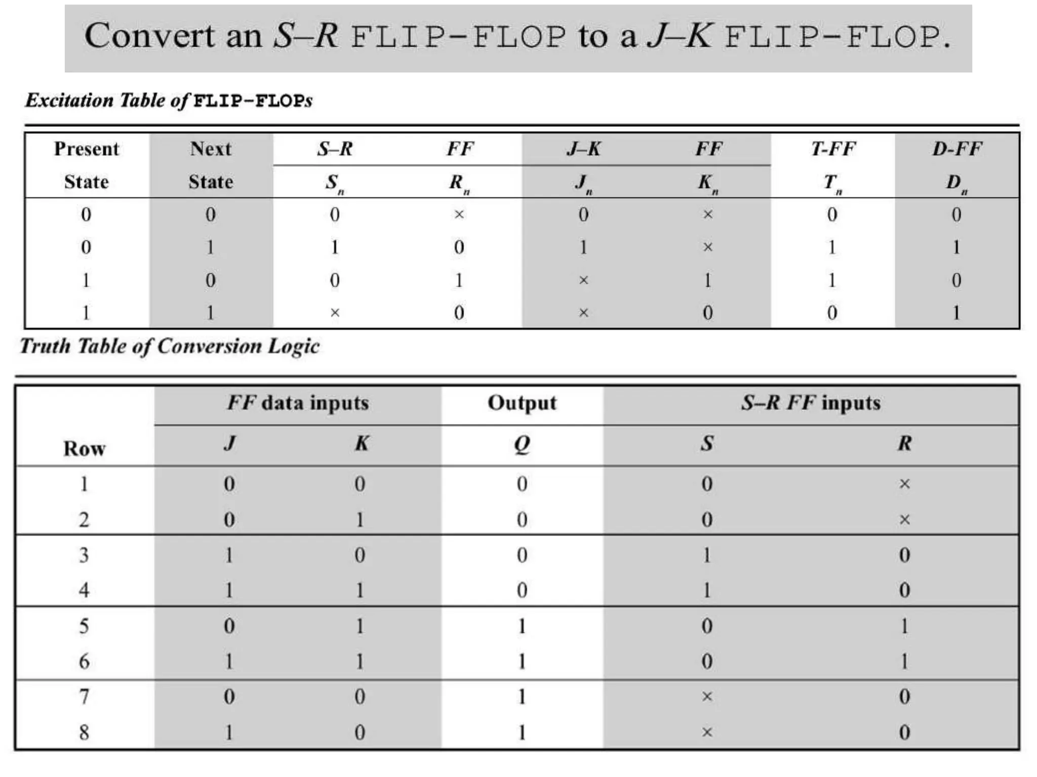
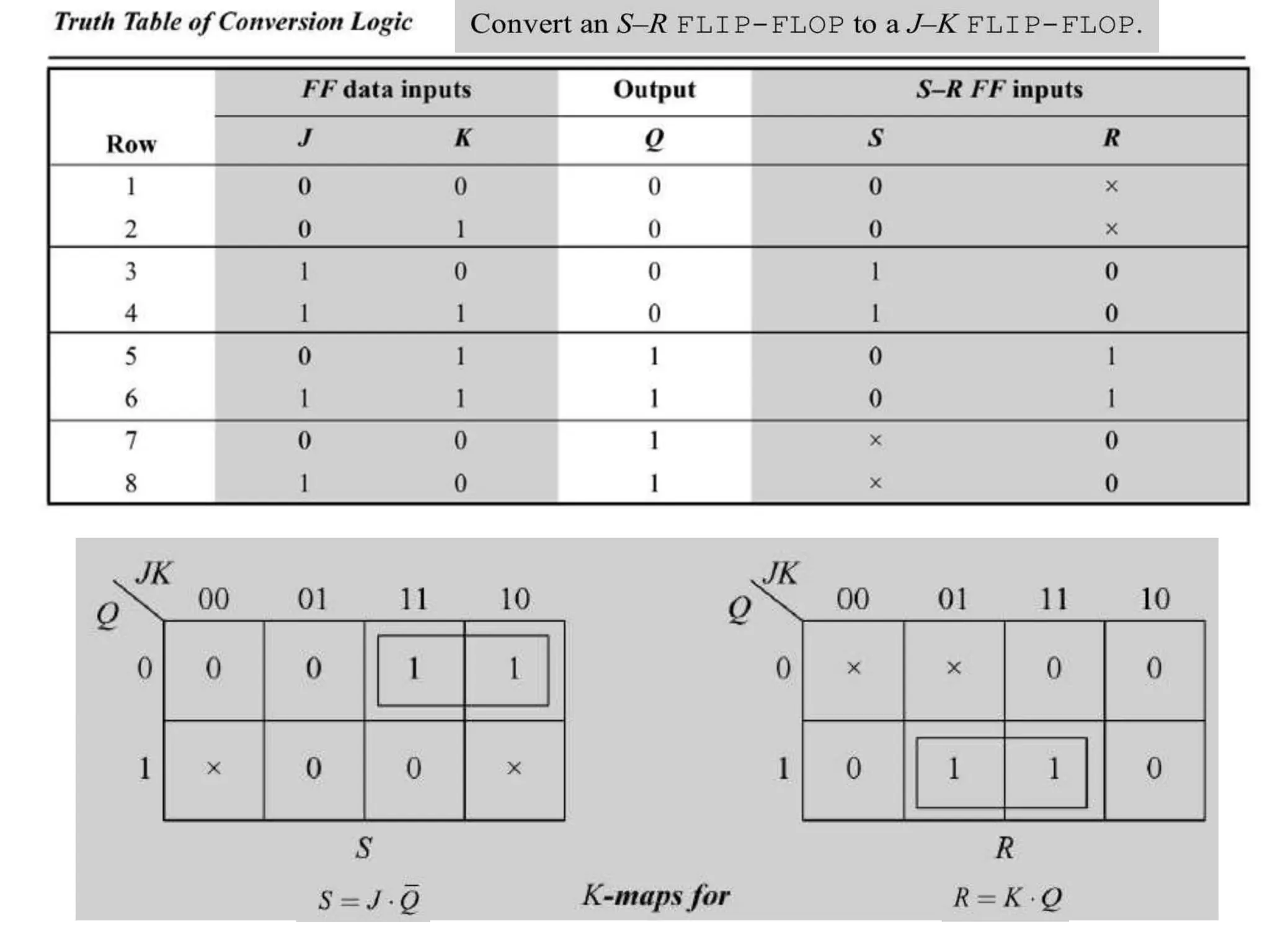
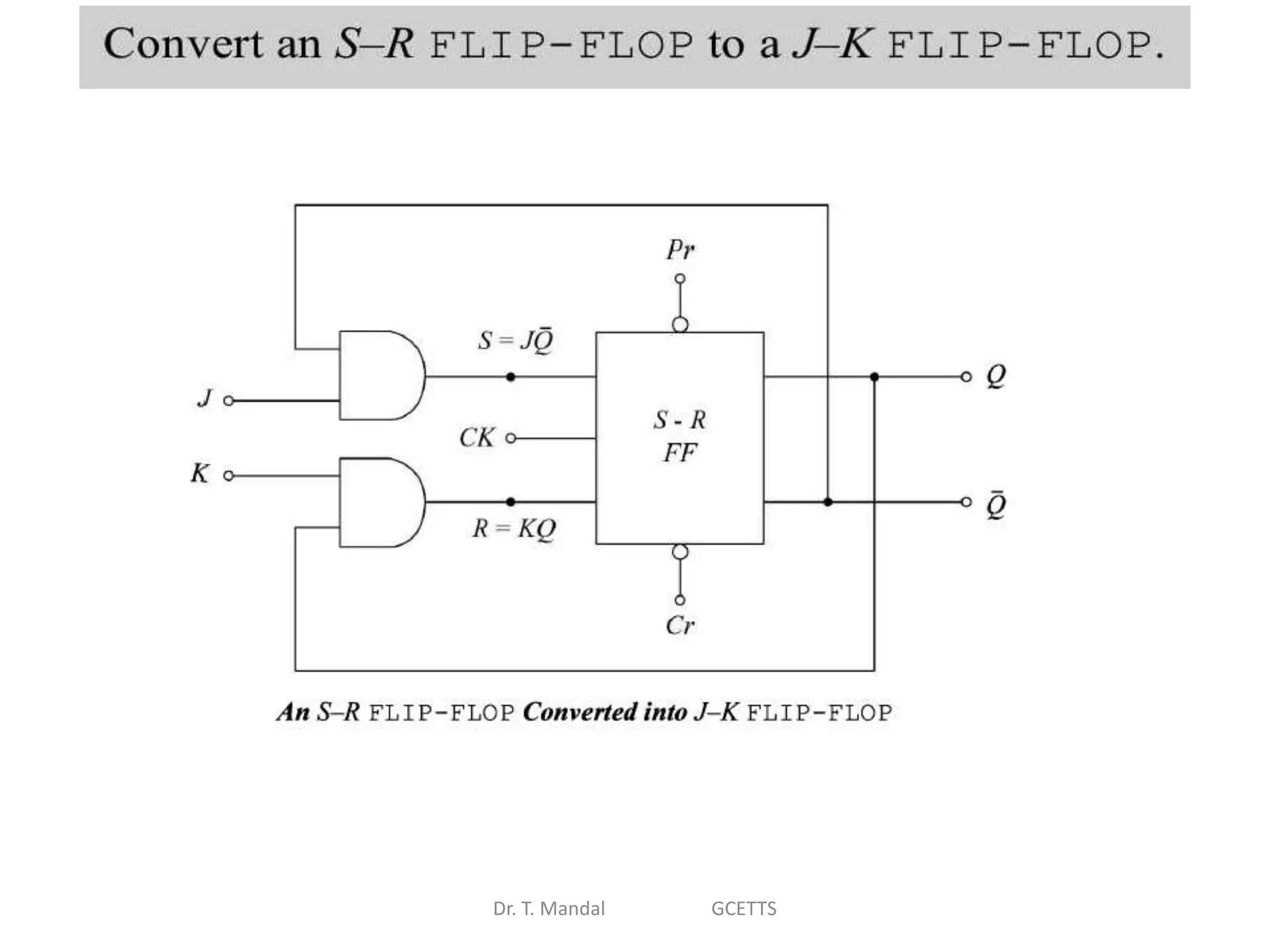
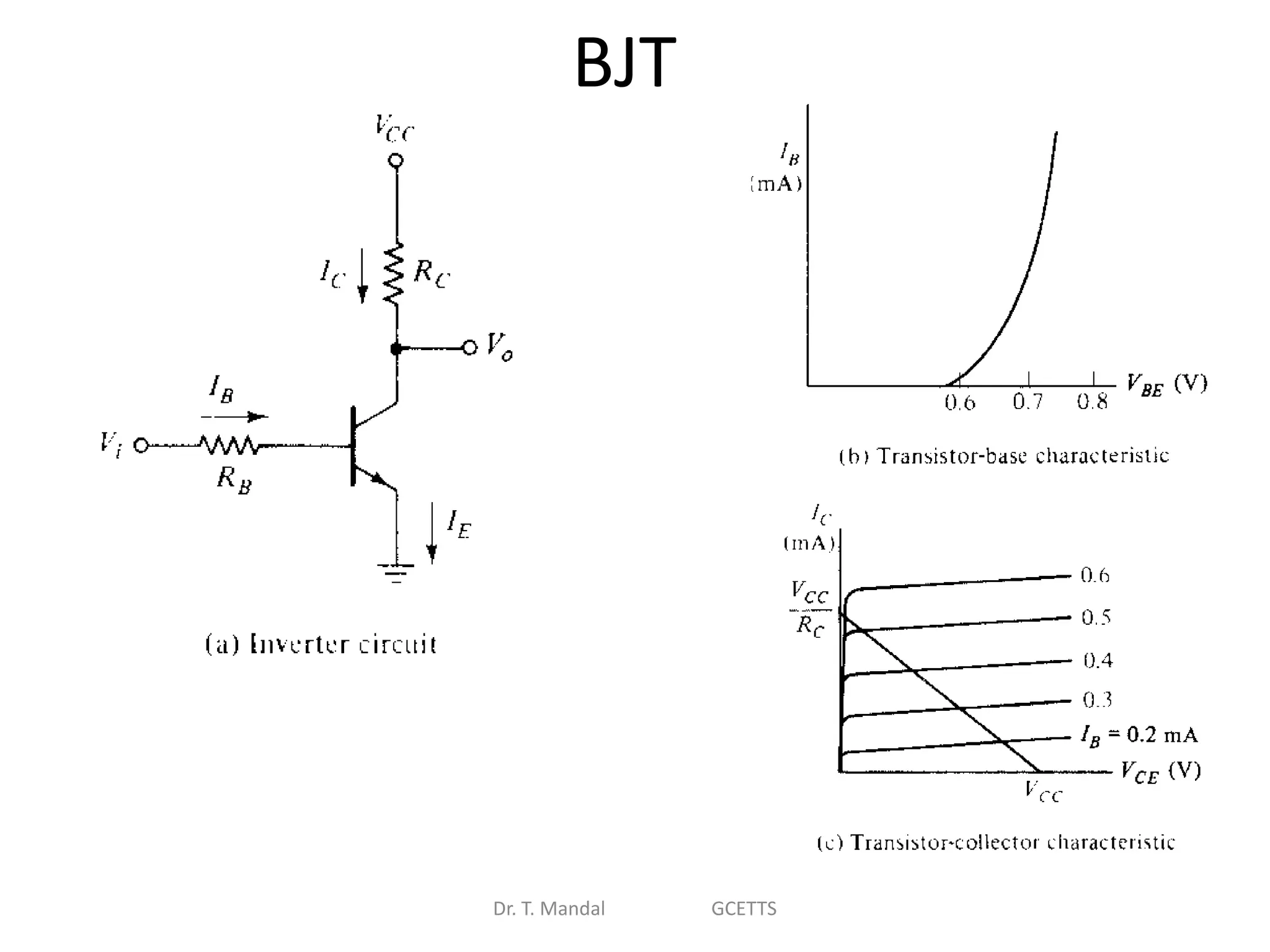
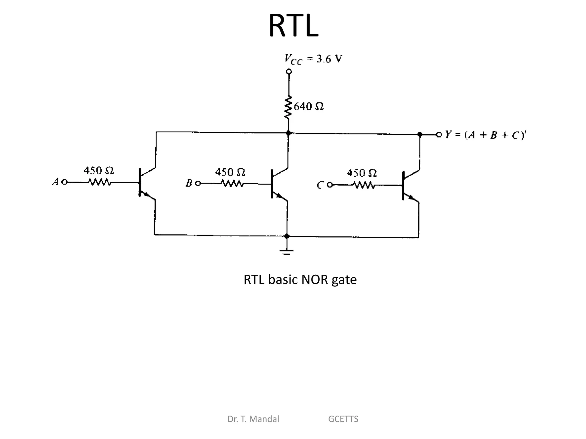
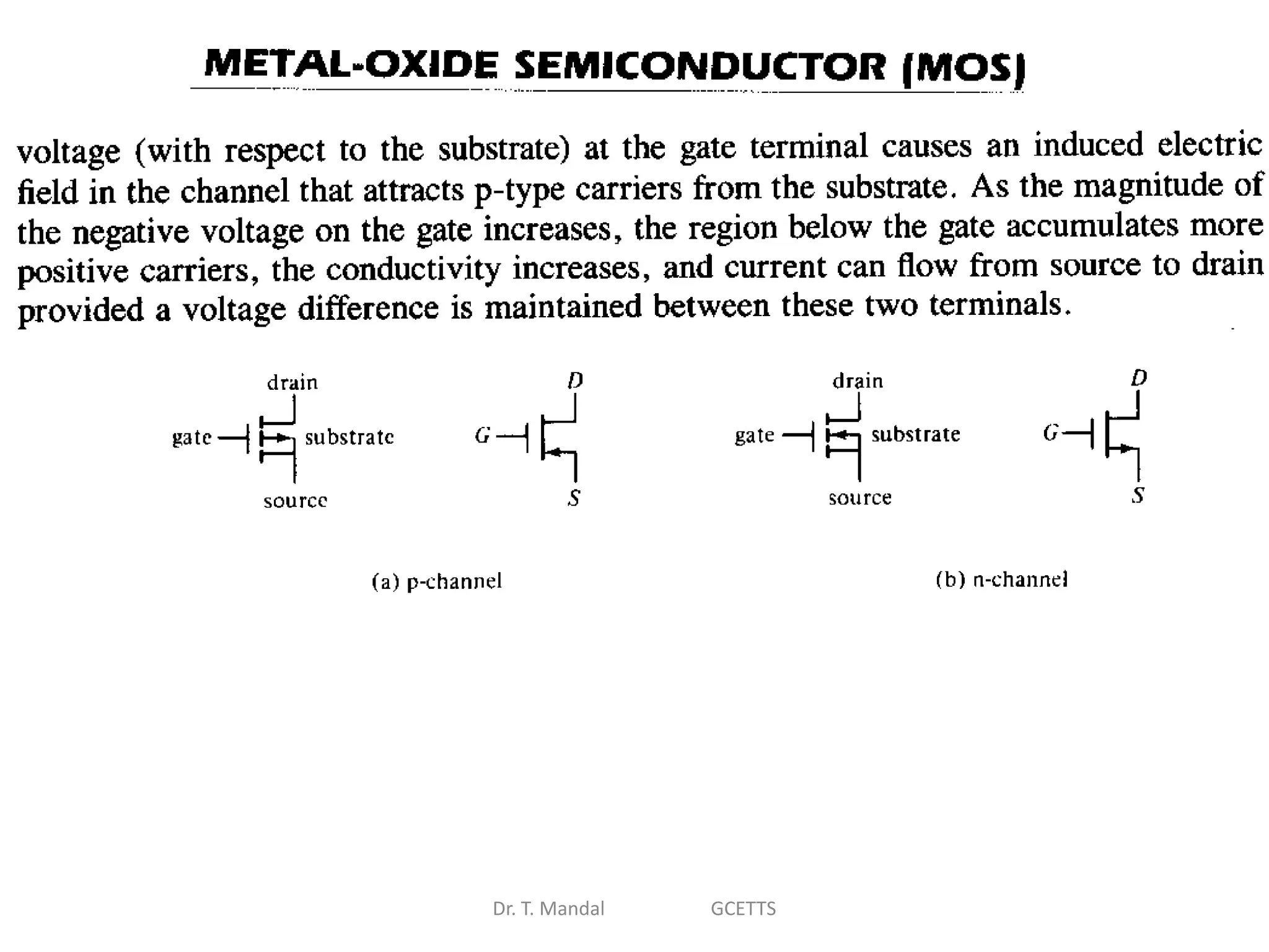
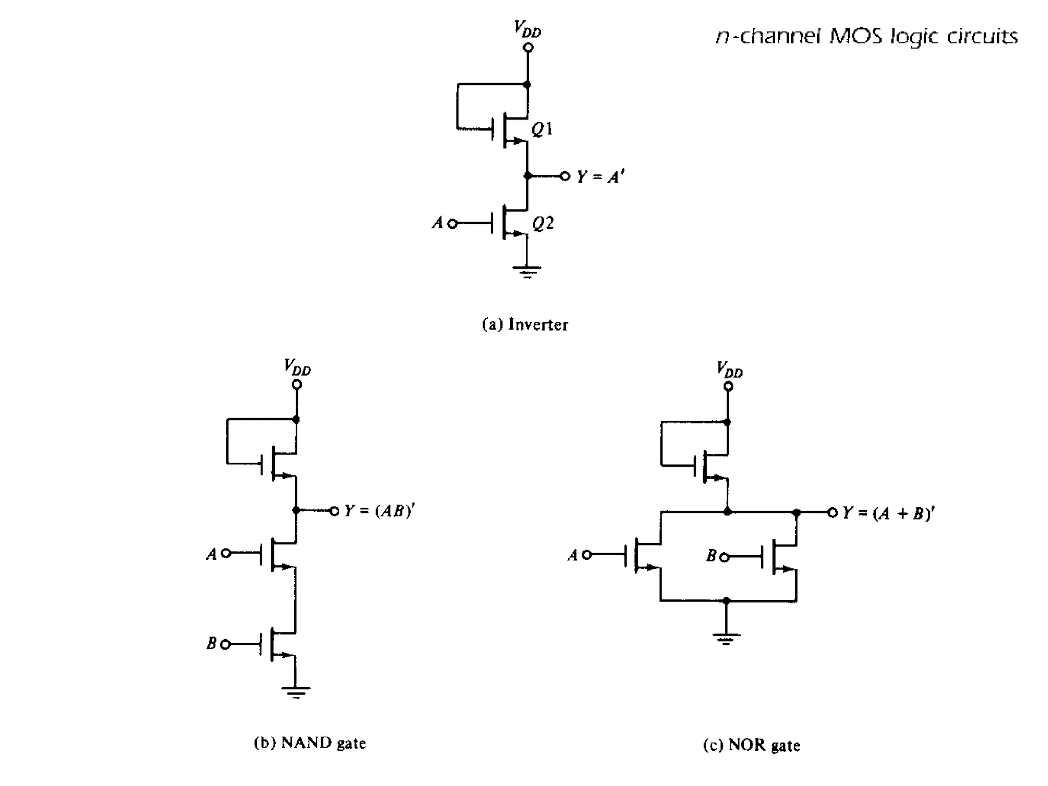
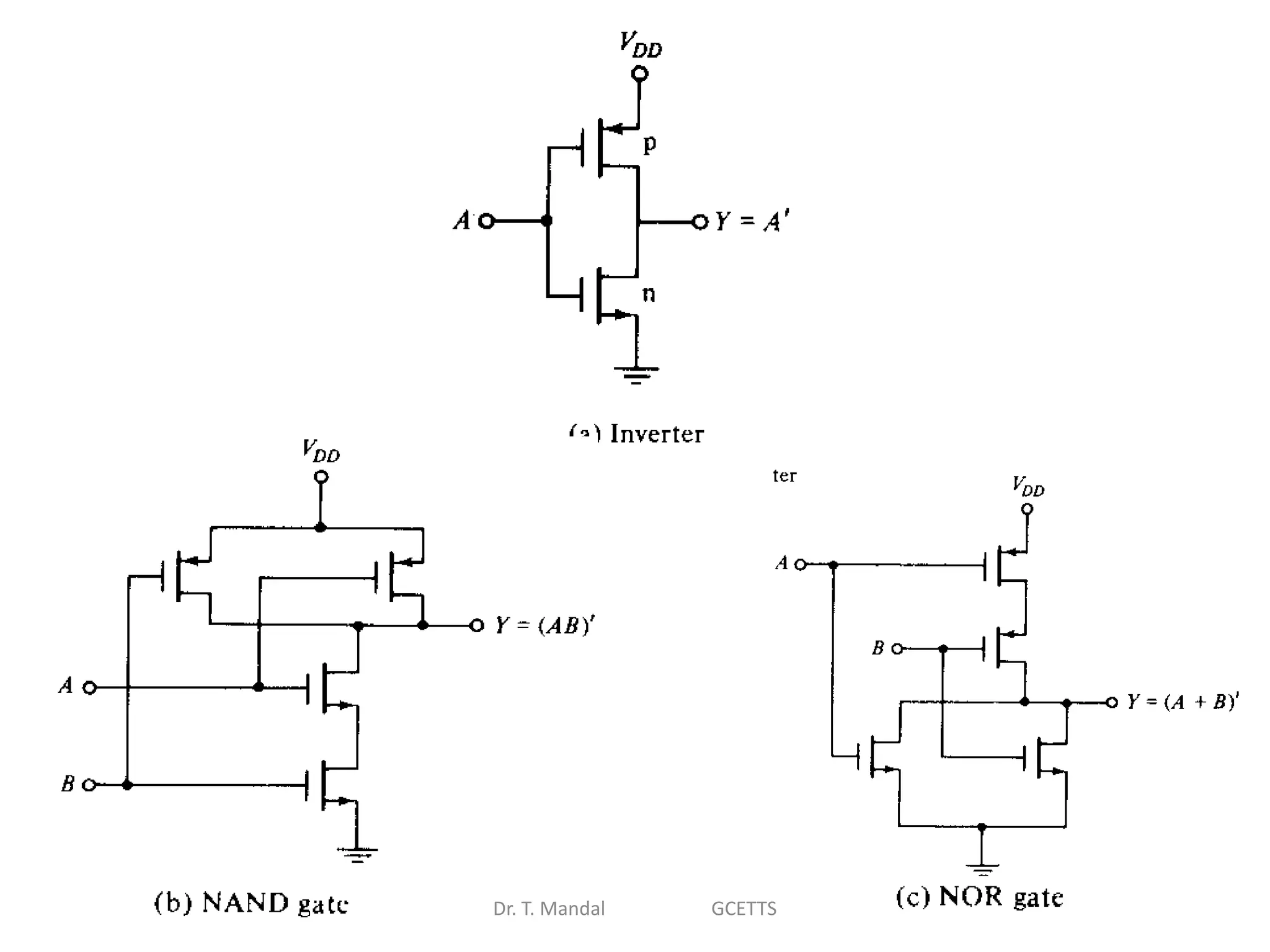
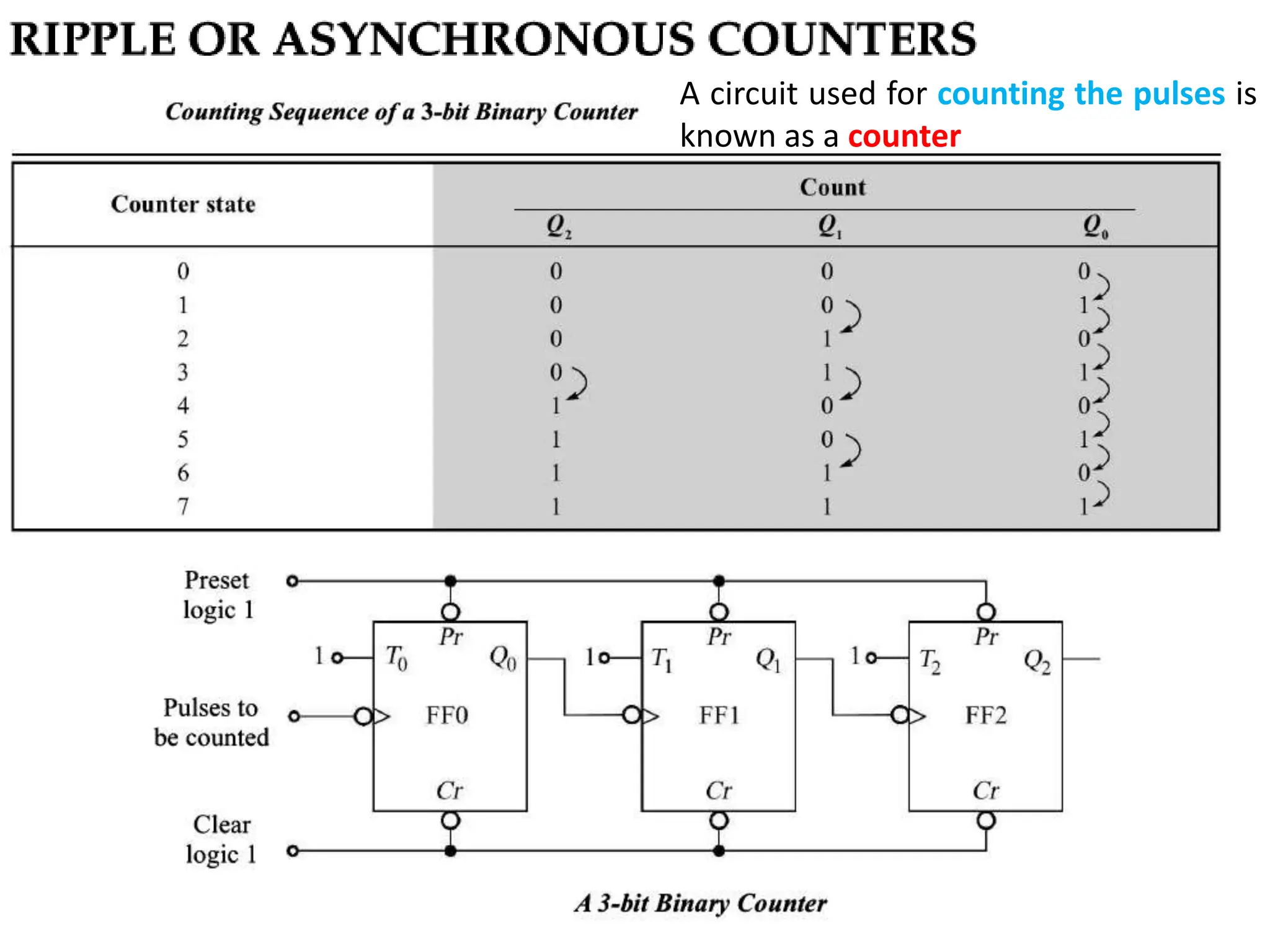
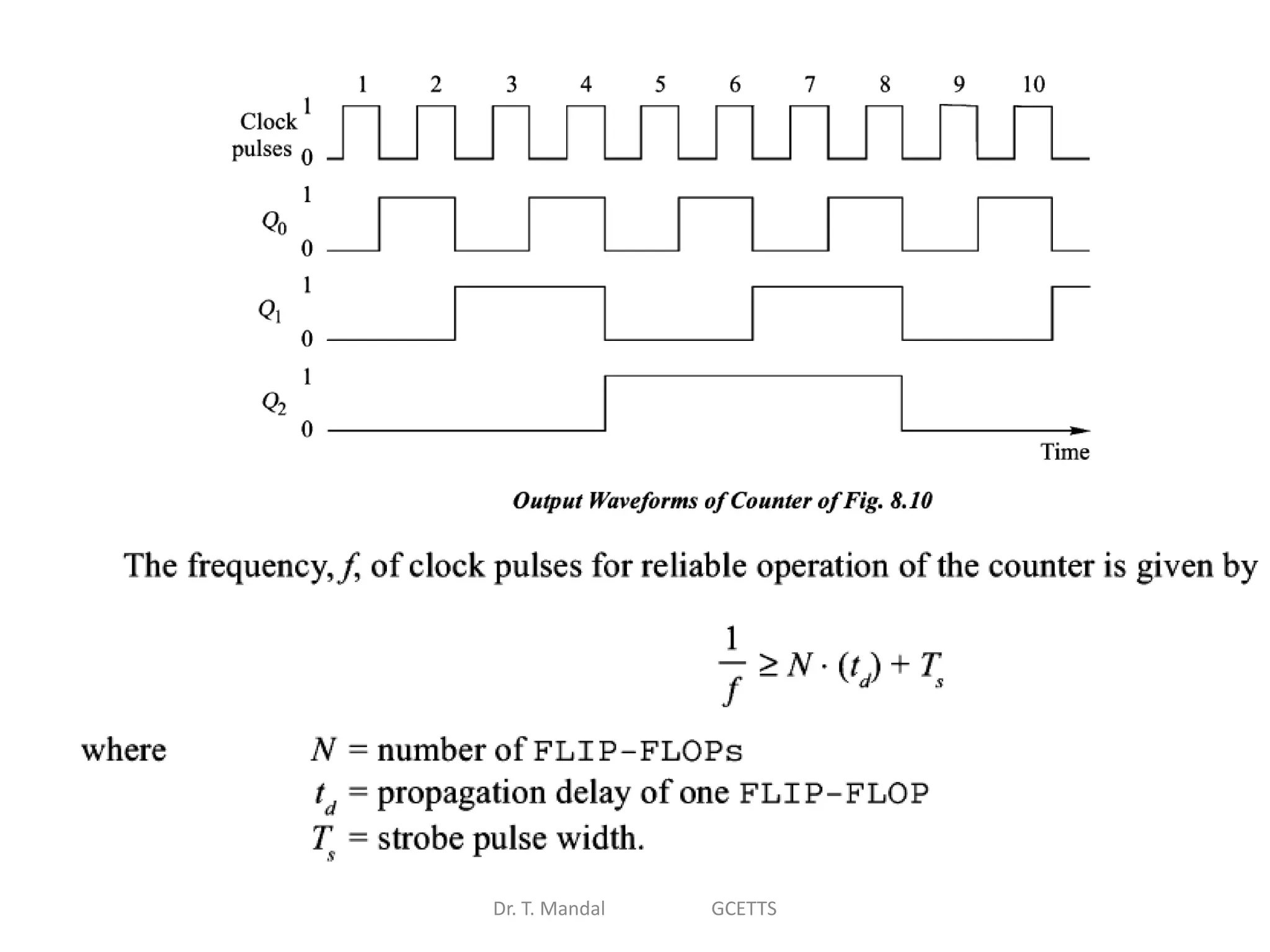
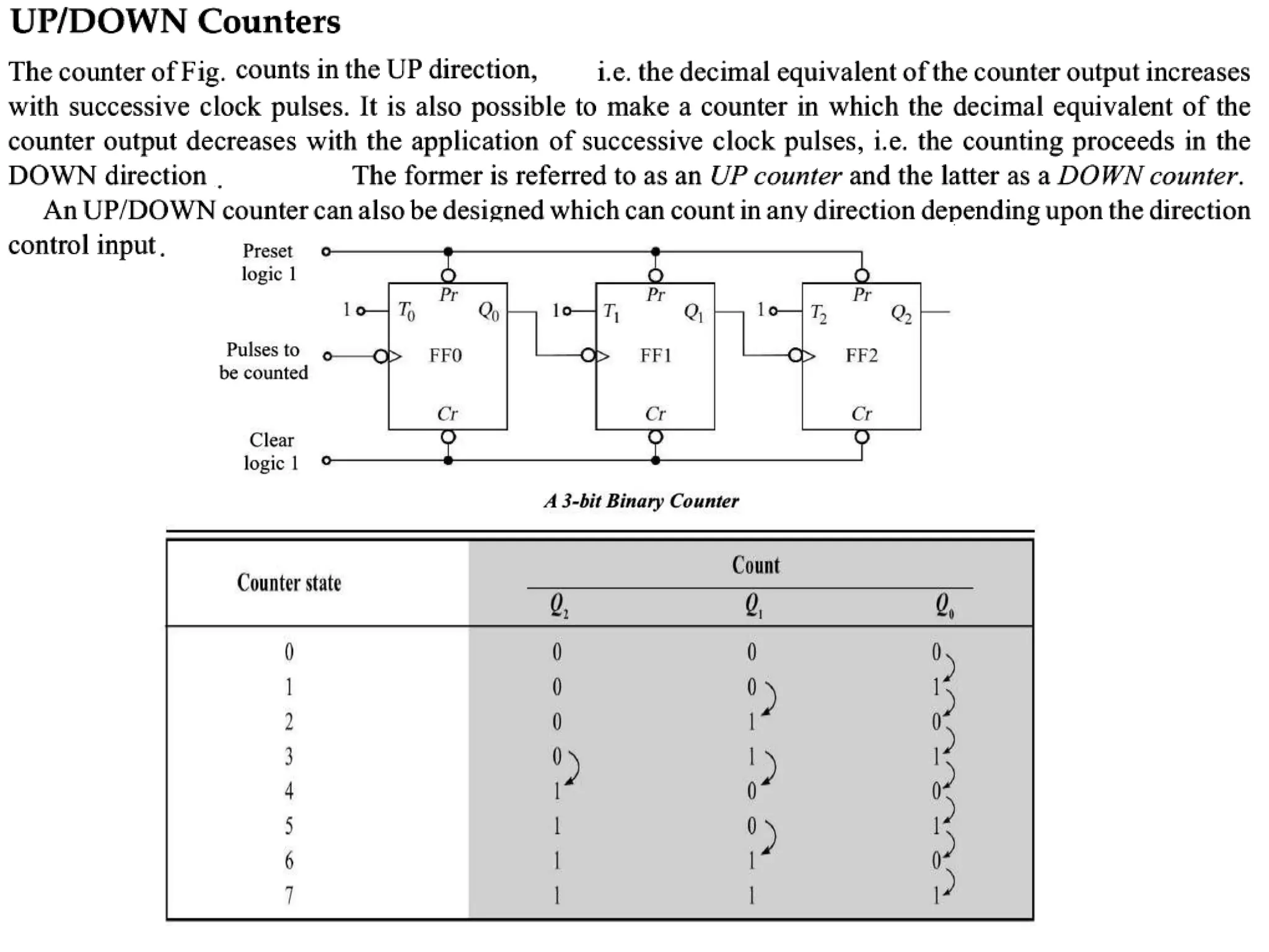
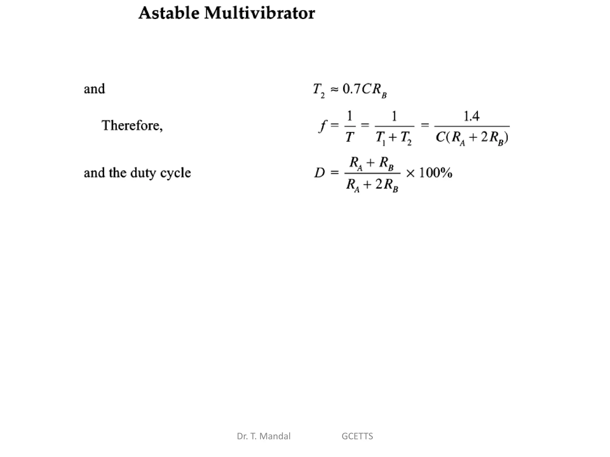
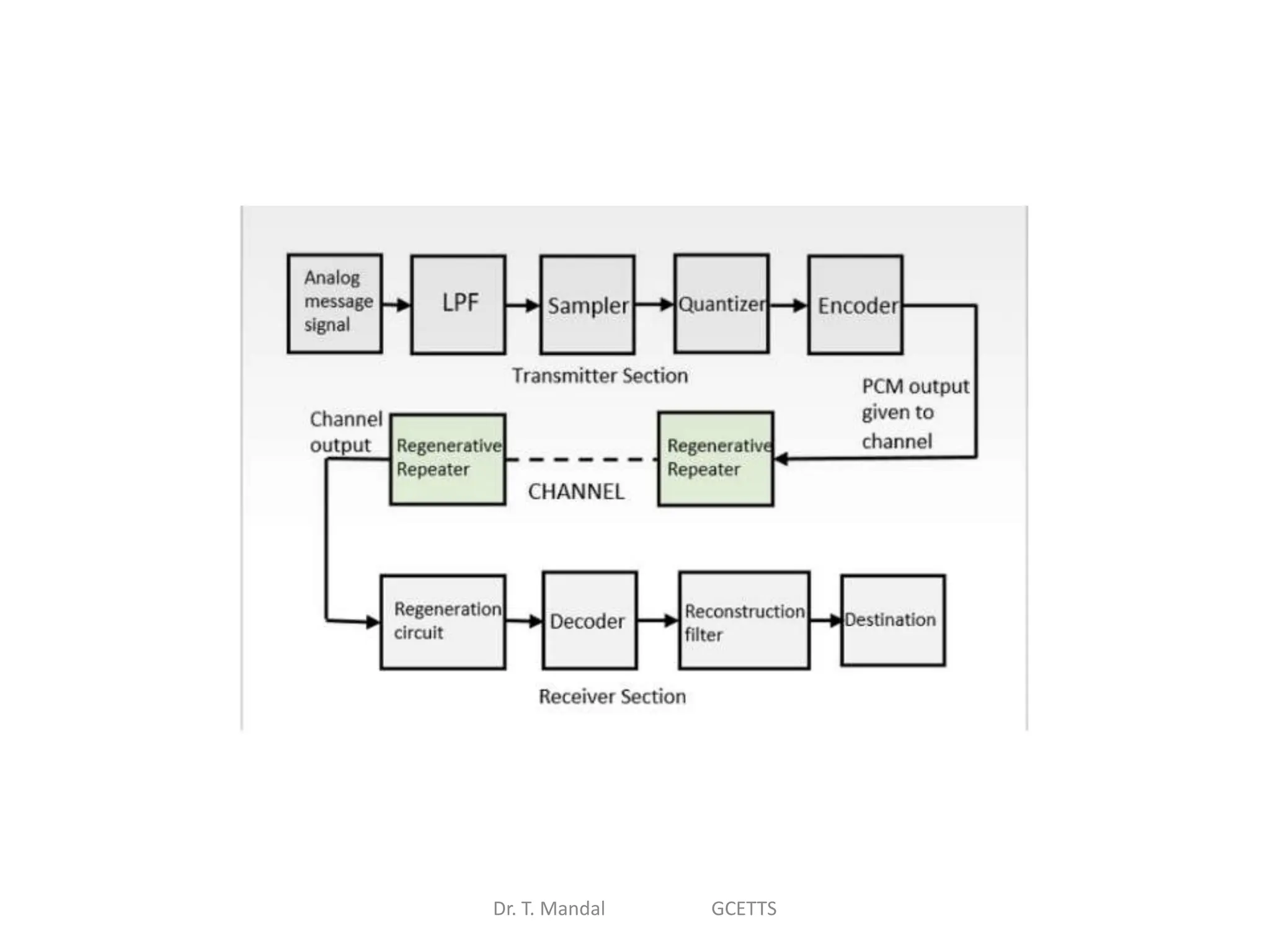
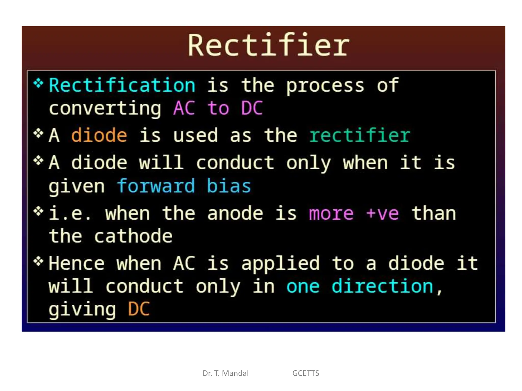
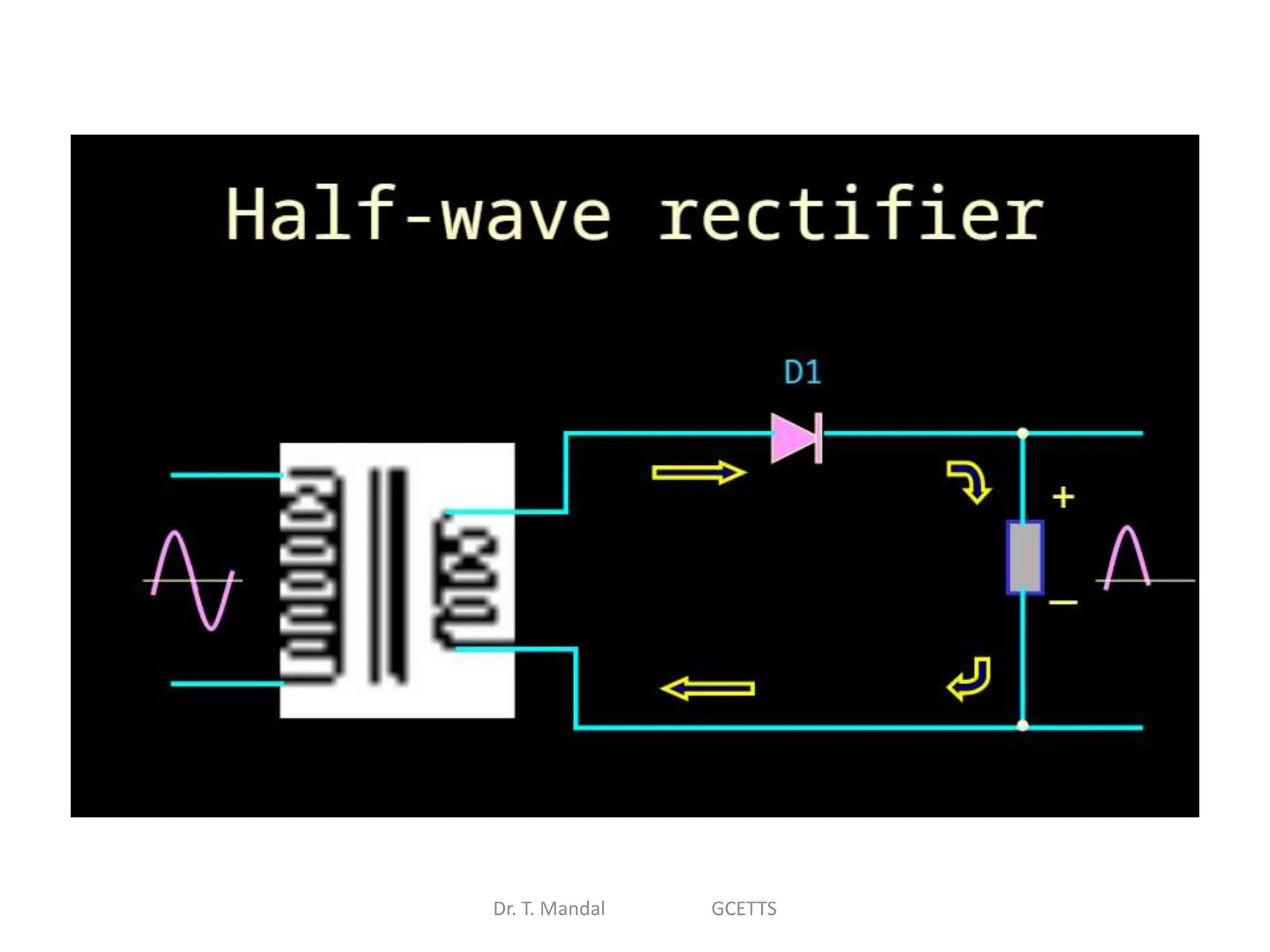
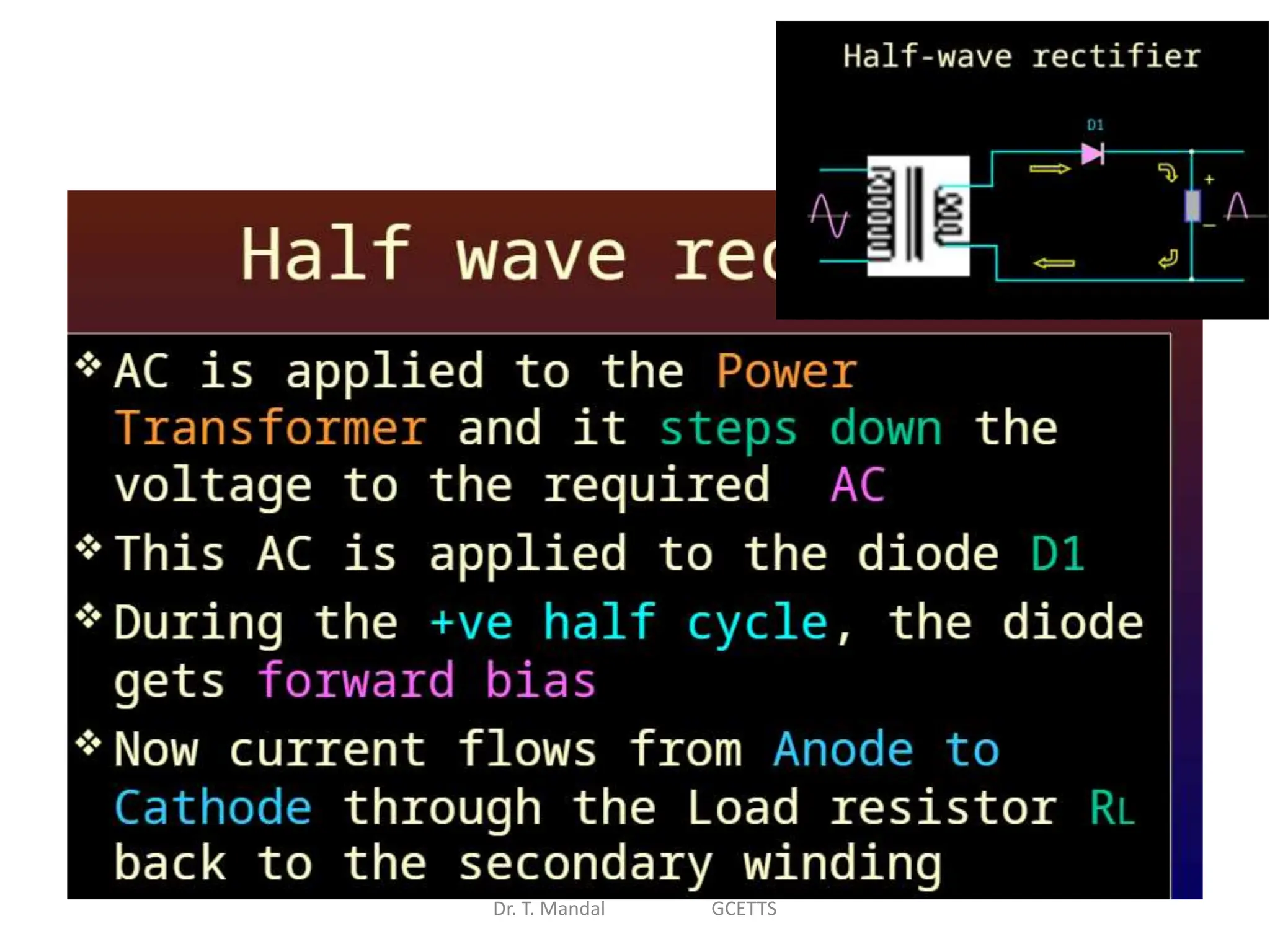
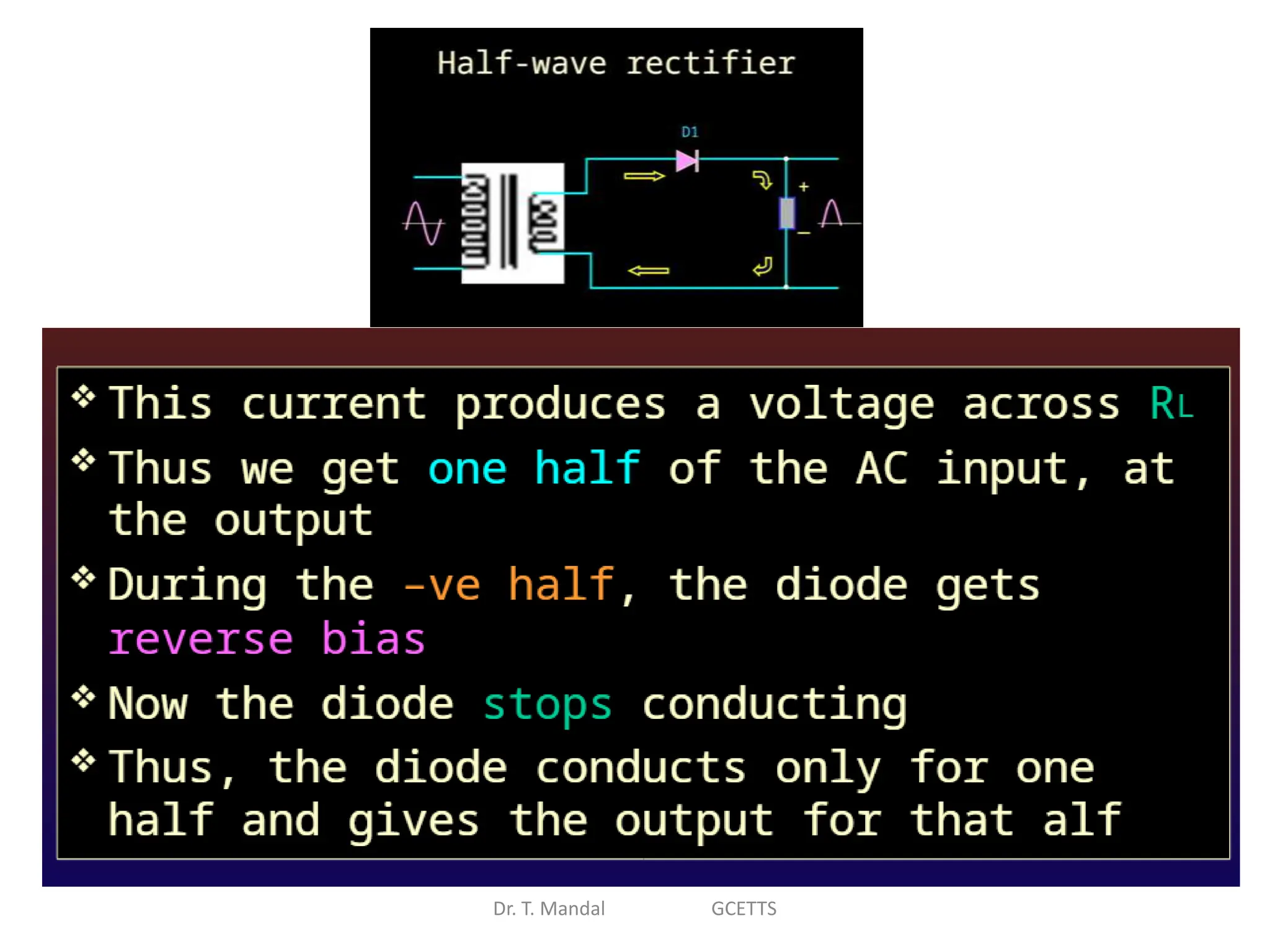
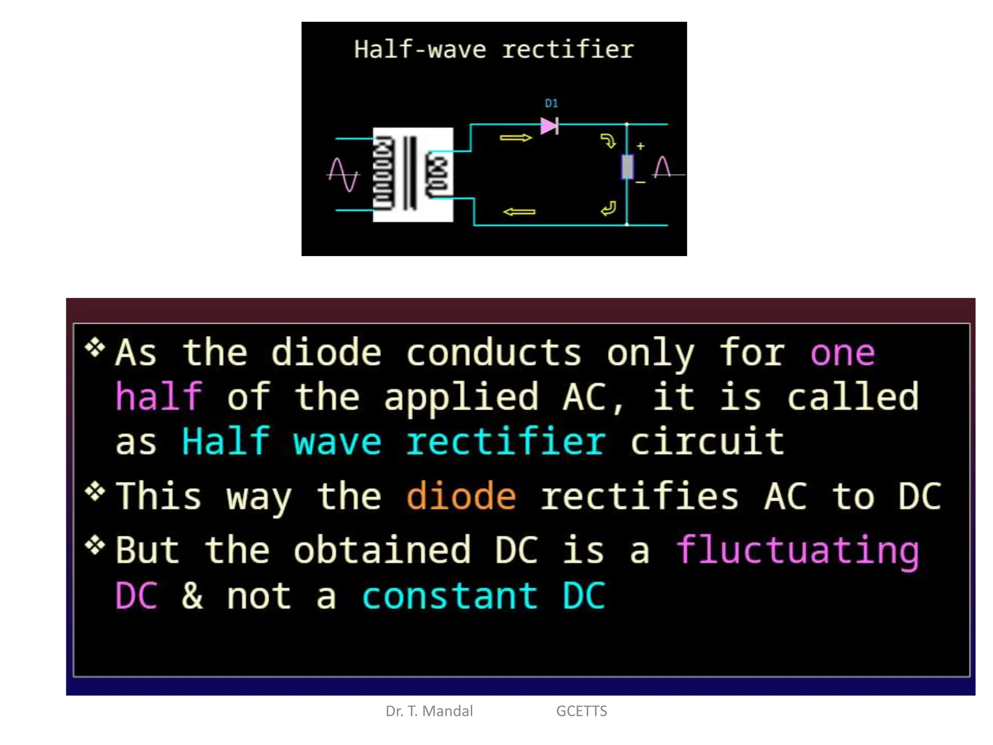
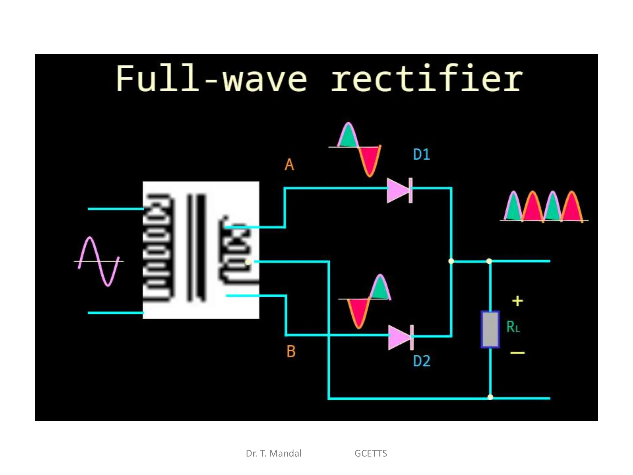
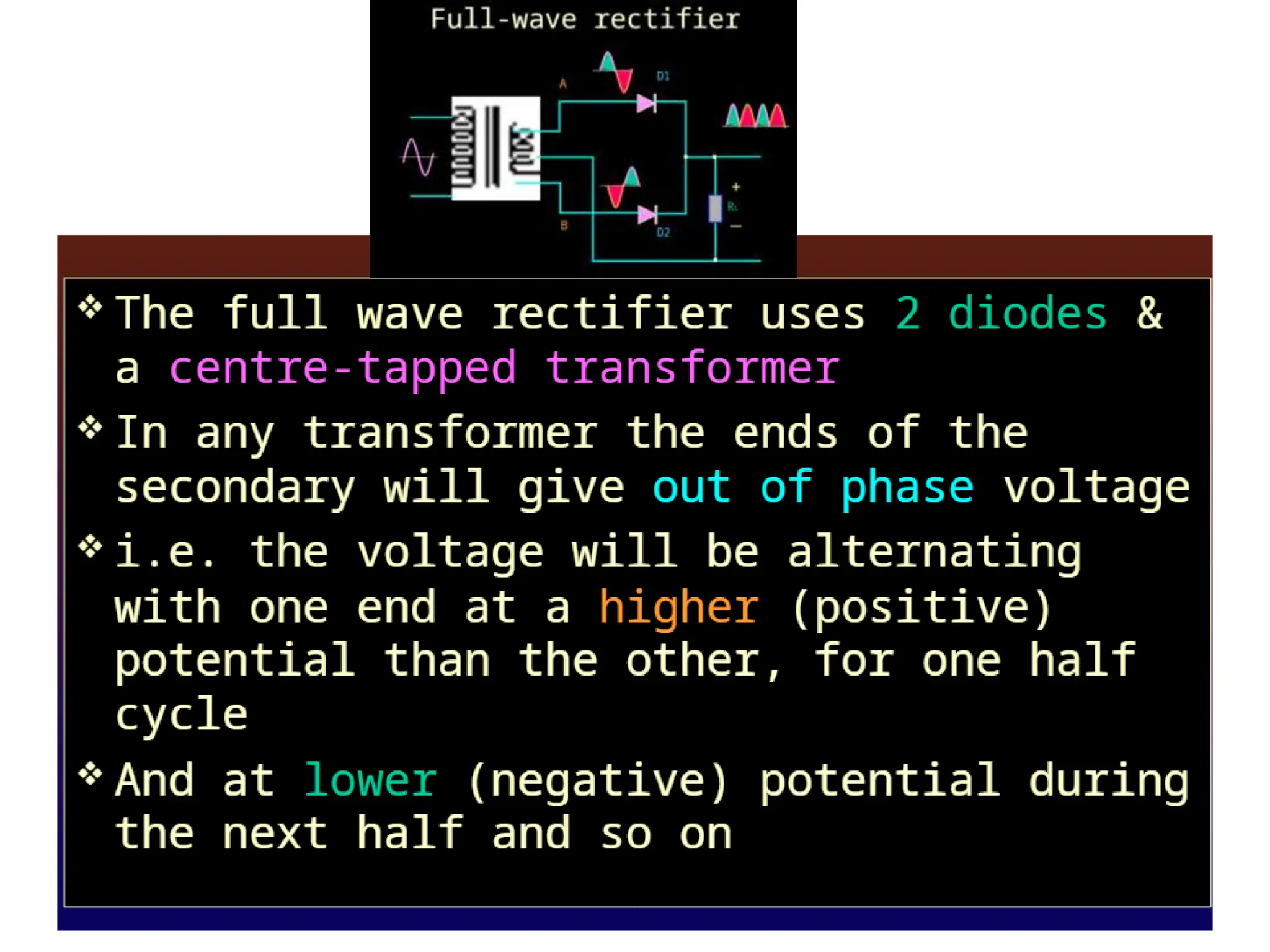
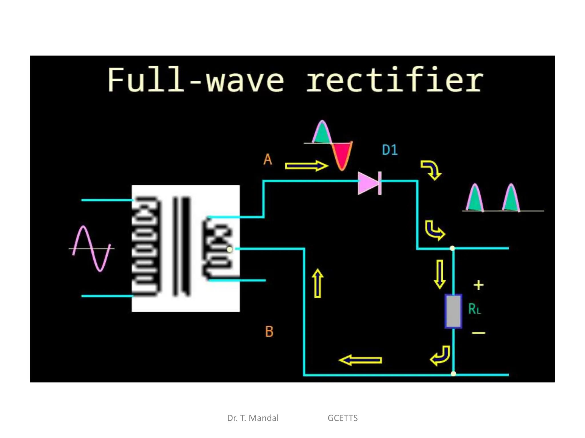
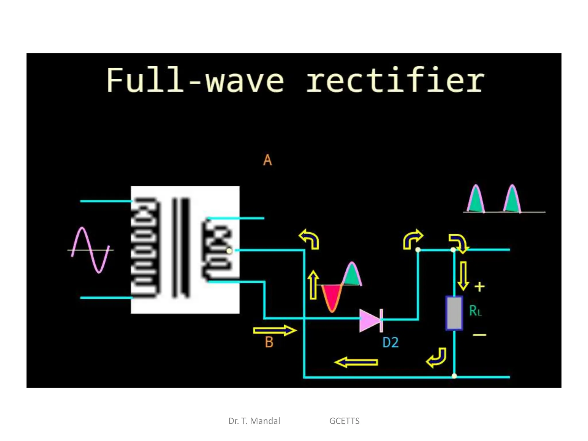
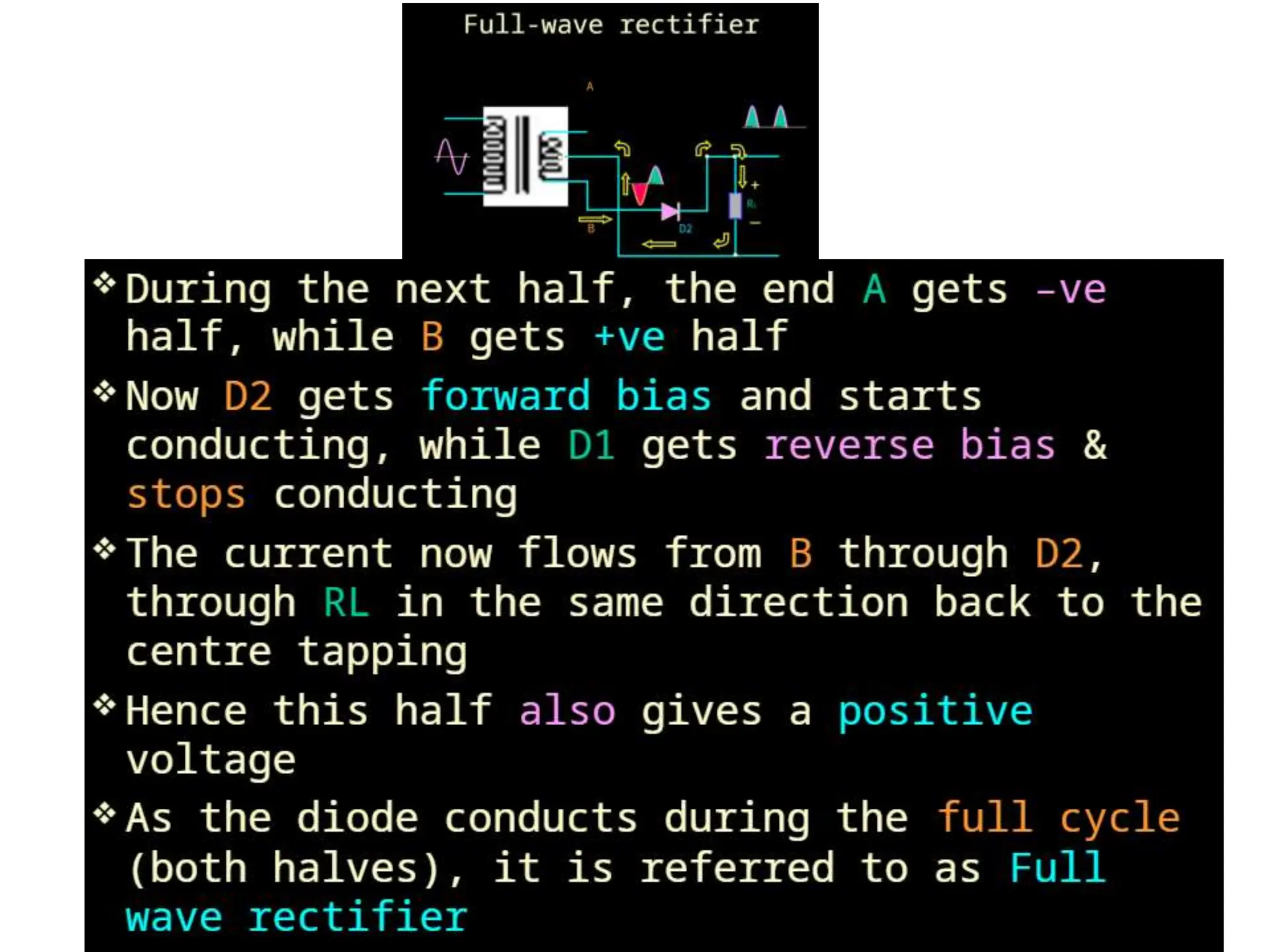
Jdjddjdjjfjrjrhhfbrhrjhjjfjrjfrifjhfjdirurfu8fi3hdudoickegdhejdofjrvdjozdkjieofiudjrhciyyfifjjvi9r7ugidof8cdukrkfj2keoekeRecombination in bacterial growth refers to the process by which bacteria exchange genetic material with each other, leading to the formation of new genetic combinations. This process can occur through several mechanisms, including transformation, conjugation, and transduction.
1. Transformation: In transformation, bacteria take up free DNA from their environment and incorporate it into their genome. This DNA may come from lysed bacterial cells or be released into the environment by other means. Once inside the cell, the foreign DNA can recombine with the bacterial chromosome, leading to genetic diversity.
2. Conjugation: Conjugation involves the direct transfer of genetic material from one bacterium to another through physical contact. This transfer typically occurs through a conjugative pilus, a structure that forms a bridge between the donor and recipient cells. During conjugation, a copy of the donor's DNA, often in the form of a plasmid, is transferred to the recipient cell, where it can integrate into the chromosome or exist as a separate genetic element.
3. Transduction: Transduction occurs when bacterial DNA is transferred from one bacterium to another by a bacteriophage (a virus that infects bacteria). During the lytic cycle of viral replication, some bacteriophages may accidentally package bacterial DNA instead of their own genome. When these phages infect other bacteria, they inject this bacterial DNA into the new host, where it can recombine with the recipient chromosome.
Recombination plays a crucial role in bacterial evolution and adaptation by facilitating the exchange of beneficial genetic traits, such as antibiotic resistance or metabolic capabilities. It contributes to the genetic diversity of bacterial populations and can influence their ability to survive and thrive in various environments.In enzymes, a domain refers to a distinct structural and functional unit that contributes to the overall activity of the enzyme. Domains are often modular components within the enzyme's overall structure, each with its own specific role or function. These functions may include substrate binding, catalysis, regulation, or interaction with other molecules. Domains can have specific shapes, surface properties, and active sites tailored to perform particular biochemical tasks within the enzyme's catalytic cycle. Additionally, enzymes can contain multiple domains, which may interact with each other to modulate enzyme activity or to confer versatility in substrate recognition and binding. The organization of domains within an enzyme contributes to its overall efficiency and specificity in catalyzing biochemical reactions.Superscalar architecture is a CPU design paradigm that enables the simultaneous execution of multiple instructions within a single clock cycle. This is achieved by having multiple execution units, allowing t
Cheap Rate ➥8448380779 ▻Call Girls In Iffco Chowk Gurgaon
Digital Logic.pptxghuuhhhhhhuu7ffghhhhhg
1. Digital Logic
Dr. T. Mandal GCETTS
+5
V
–5
Ti me
+5
V
–5
1 0 1
Time
Analog:
values vary over a broad range
continuously
Digital:
Only assumes discrete values
2. Dr. T. Mandal GCETTS
Closure
A set S is closed w.r.t a binary number operator if, for every pair
of elements of S, the binary operator specifies a rule for
obtaining a unique element of S
• For example, the set of natural number N={1,2,3,4,…….} is
closed w.r.t the binary operator plus (+) by the rule
arithmetic addition. Since for any a, b ∈ N by the operation
a + b = c.
• The set of natural number is not closed w.r.t the binary
operator minus (-) by the rule of arithmetic subtraction
because 2-3 = -1 and 2,3 ∈ N, while (-1) N
CommutativeLaw:
A binary operator * on a set S is said to be Commutative whenever
x*y=y*x for all x, y ∈ 𝑆
3. Dr. T. Mandal GCETTS
Identity element
A set S is said to have an identity element w.r.t a binary operator
*on S if there exists an element e ∈ S with the property
e*x = x*e = x for every x ∈ S
4. Dr. T. Mandal GCETTS
Inverse
A set S having the identity element e w.r.t a binary operator * is
said to have an inverse whenever, for every x ∈ S, there exists an
element y ∈ S such that
x*y = e
Example: In the set of integers I with e = 0, the inverse of an
element a is (-a) since a+(-a) = 0
8. Postulates and Theorem of Boolean Algebra
Postulate 1 (a) x + 0 = x (b) x . 1 = x
Postulate 5 (a) x + x’ = 1 (b) x . x’ = 0
Theorem 1 (a) x + x = x (b) x . x = x
Theorem2 (a) x+1 = 1 (b)x.0 = 0
Theorem3, Involution (a) (x’)’ = x (b)
Postulate 3, commutative (a) x + y = y + x (b) x y = yx
Theorem 4, associative (a) x+(y+z) = (x+y)+z (b) x(yz) =(xy)z
Postulate 4, distributed (a) x(y+z)=xy+xz (b)x+yz=(x+y)(x+z)
Theorem 5, Demorgan (a) (x+y)’ = x’y’ (b) (xy)’= x’+y’
Theorem 6, absorption (a) x+xy = x (b) x(x+y) = x
Dr. T. Mandal GCETTS
9. Example 1: Simplify the Boolean functions
to a minimum literals
1. X+X’Y = (X+Y)
2. X(X’+Y) = XY
3. X’Y’Z+X’YZ+XY’ = (X’Z+XY’)
4. XY+X’Z+YZ = (XY+X’Z)
5. (X+Y)(X’+Z)(Y+Z) = (X+Y)(X’+Z)
Dr. T. Mandal GCETTS
10. Solution of Example 1
1. X+X’Y =(X+X’)(X+Y) = 1.(X+Y) = X+Y
2. X(X’+Y) = XX’+XY = 0+XY
3. X’Y’Z+X’YZ+XY’= X’Z(Y’+Y)+XY’=X’Z+XY’
4. H.W
5. H.W Dr. T. Mandal GCETTS
11. Complement of Function
Dr. T. Mandal GCETTS
The complement of a function F is F’
The complement of function is obtained from an
interchange of 0’s for 1’s and 1’s for 0’s in the
value of F.
The complement of a function may be derived
algebraically through De Morgan’s theory.
The three – variable form of the first De Morgan’s
theory
14. Complement of Function
Dr. T. Mandal GCETTS
A simpler procedure for deriving the
complement of a function is to take the dual
of the function and complement each literal
This method follows from the generalized
De Morgan’s theorem
The dual of a function is obtained from
the interchange of AND and OR operators
and 1’s and 0’s
15. Complement of Function
Dr. T. Mandal GCETTS
Example: Find the complement of the functions F1 and F2 of
previous example
By taking their duals and complementing each literals
16. Canonical and Standard Forms
Dr. T. Mandal GCETTS
X’Y’
X’Y
XY’
XY
}
Two binary variables X and
Y combined with an OR
operation
Minterm
X+Y
X+Y’
X’+Y
X’+Y”
}
Maxterm
Two binary variables X and
Y combined with an AND
operation
Minterm or Maxterm determine by = 2^n for n variable
The binary numbers from 0 to 2^n – 1.
If n = 2, term = 4 & Binary numbers: 0 to 3
18. Dr. T. Mandal GCETTS
Canonical and Standard Forms
A Boolean function may be expressed algebraically
from a given truth table by forming a minterm for
each combination of the variables which produces
a 1 in the function.
Taking the OR of all those terms
20. Canonical and Standard Forms
Dr. T. Mandal GCETTS
A Boolean function may be expressed algebraically
from a given truth table by forming a maxterm for
each combination of the variables which produces
a O in the function.
Taking the AND of all those terms
21. Canonical and Standard Forms
Dr. T. Mandal GCETTS
Boolean function expressed as a sum of minterms or product of maxterm
are said to be in canonical form
22. Canonical and Standard Forms
Dr. T. Mandal GCETTS
Sum of Minterm
For n variable, Minterm = 2^n
Boolean function can be expressed as a sum of minterms
The minterm's whose sum defines the Boolean function
are those that give the 1’s of the function in a truth
table.
Example: Express the Boolen function F = A+B’C in a Sum of
Minterm
23. Canonical and Standard Forms
Dr. T. Mandal GCETTS
Boolen function F = A + B’C
(I) (II)
The function has three variables A, B, and C
The first term A is missing two variables;
𝐴 = 𝐴(𝐵 + 𝐵)= AB+A𝐵
This is still missing one variables:
25. Canonical and Standard Forms
Dr. T. Mandal GCETTS
An alternate procedure for deriving the minterms of a
Boolean function is to obtain the truth table of the
function directly from the algebraic expression and then
read the Minterms from the truth table.
Consider the Boolean function given in Previous Example
Boolen function F = A+B’C
The truth table shown in Table can be derived
directly from the algebraic expression by listing
the eight binary combinations under variable
A,B and C and inserting 1’S under F for those
combination where A = 1 and BC = 01
We can read the five minterm of the function
1,4,5,6,and 7
26. Canonical and Standard Forms
Product of Maxterm
Dr. T. Mandal GCETTS
Distributed law
= x+yz=(x+y)(x+z)
28. Canonical and Standard Forms
Dr. T. Mandal GCETTS
Conversion between canonical forms
The complement of a function expressed as the sum of minterms equals
the sum of minterms missing from the original function.
This is because the original function is expressed by those minterms that
make the function equal to 1, whereas its complement is a 1 for those
minterm that the function is a 0.
Example
29. Canonical and Standard Forms
Dr. T. Mandal GCETTS
Conversion between canonical forms
The conversion between the product of maxterms and sum of
minterm is similar.
To convert from one canonical form to another, interchange the
symbols 𝒂𝒏𝒅 𝒂𝒏𝒅 list those numbers missing from the
original form.
A product of maxterm form
𝐹(𝑥, 𝑦, 𝑧) = (0,2,4,5)
Its conversion to sum of minterms is:
𝐹(𝑥, 𝑦, 𝑧) = (1,3,6,7)
.
Note:
Find the missing terms
Total number of minterms or maxterms
30. Standard Forms
Dr. T. Mandal GCETTS
The two canonical forms of Boolean algebra are basic
forms that one obtains from reading a function the
Truth Table
There are two types of standard forms:
i. Sum of Products(SOP) ii. Products of Sum (POS)
Sum of Products (SOP) is a Boolean expression
contacting AND terms, called product terms of one or
more literals each. The sum denotes the ORing of these
terms
A function expressed in sum of products is:
𝐹1 = 𝑦 + 𝑥𝑦 + 𝑥 𝑦𝑧
The expression has three product terms of one, two and three
literals each respectively. The sum is in effect an OR operation.
31. Standard Forms
Dr. T. Mandal GCETTS
Product of Sum (POS) is a Boolean expression contacting
OR terms, called sum terms of one or more literals each.
The product denotes the ANDing of these terms
A function expressed in product of sums is:
𝐹2 = 𝑥 𝑦′ + 𝑧 (𝑥′ + 𝑦 + 𝑧′ + 𝑤)
The expression has three sum terms of one, two and three literals
each respectively. The products is in an AND operation.
The use of the words products and sum stems from the similarities
of the AND operation to the arithmetic product (multiplication) and
the similarities of the OR operation to the arithmetic sum
32. Non-standard Forms
Dr. T. Mandal GCETTS
A Boolean function may be expressed in a nonstandard form
The function is neither SOP nor in POS form
It can be changed to a standard form by using the distributive law
to remove the parentheses:
33. Boolean Algebra and Logical Operators
Algebra: variables, values, operations
In Boolean algebra, the values are the symbols 0and 1
If a logic statement is false, it has value 0
If a logic statement is true, it has value 1
Operations: AND, OR, NOT
Dr. T. Mandal GCETTS
38. Simplification of Boolean Functions
m0 m1
m2 m3
Dr. T. Mandal GCETTS
00/x’y’
m0
01/x’y
m1
10/xy’
m2
11/xy
m3
y
X
0 1
Y’ y
0 x’
1 x
Fig. Two variable map
• There are four minterms for two variables
• Map consists four squares, one for each minterm
X Y Minter
m
Design
-ation
0 0 X’Y’
m0
0 1 X’Y
m1
1 0 XY’
m2
1 1 XY
m3
39. Simplification of Boolean Functions
Dr. T. Mandal GCETTS
• There are eight minterms for three variables
• Map consists eight squares, one for each minterm
m0 m1 m3 m2
m4 m5 m7 m6
40. Simplification of Boolean Functions
Dr. T. Mandal GCETTS
Example
F(x,y,z)= 𝟐, 𝟑, 𝟒, 𝟓 = 𝒙′𝒚 + 𝒙𝒚′
x’y
xy’
m0 m1 m3
1
m2
1
m4
1
m5
1
m7 m6
41. Simplification of Boolean Functions
Dr. T. Mandal GCETTS
Example
yz
xz’
𝐹(𝑥, 𝑦, 𝑧) = 3,4,6,7 = 𝑦𝑧 + 𝑥𝑧′
42. Simplification of Boolean Functions
Dr. T. Mandal GCETTS
The number of adjacent squares that may be combined must
always represent a number that is power of two (2^n)such
as 1, 2, 4 and 8.
As larger number of adjacent squares are combined, we
obtain a product term with fewer literals
One square represents one minterm, giving a term of
three literals
Two adjacent square represent a term of two literals
Four adjacent square represent a term of one literals
Eight adjacent squares encompass the entire map and
produce a function that is always equal to 1
48. Dr. T. Mandal GCETTS
The procedure for combining squares in the map may be made
more systematic if we understand the meaning of the terms
referred to as prime implicant.
A prime implicate is a product term obtained by combining the
maximum possible number of adjacent squares in the map. If a
minterm in a square is covered by only one prime implicate, the
prime implicate is said to be essential.
The prime implicants of a function can be obtained from the map
by combining all possible maximum numbers of squares.
This means that a single 1 on a map represents a prime
implicant if it is not adjacent to any other 1’s.
Two adjacent 1’s form a prime implicant provided they are
not within a group of four adjacent squares.
Four adjacent 1’s form a prime implicant if they are not
within a group of eight adjacent squares, and so on.
50. Dr. T. Mandal GCETTS
The 1’s marked in the map represents all the minterms of the function.
The squares marked with 0’s represent the minterms not included in F, therefore
denote the complement of F or F’.
51. Dr. T. Mandal GCETTS
Combining the squares with 1’s gives the simplified function in sum of product.
1 1 1
1
1 1 1
55. Dr. T. Mandal GCETTS
Logic circuits for digital system may be
combination and sequential
A combinational circuit consists of logic gates whose
outputs at any time are determined directly from the
present combination of inputs without regard to previous
inputs.
56. ADDER
Dr. T. Mandal GCETTS
Digital computer perform a verity of information processing task .
Among the basic function are the various arithmetic operations.
The most basic arithmetic operation is addition of two binary digit
The simple addition consists of four possible elementary operation,
namely
0+0= 0; 0+1 = 1; 1+0 = 1; 1+1= 10
The first three operations produce a sum whose length is one
digit
When both augend and addend bits are equal to 1, the binary
sum consists of two digits
The higher significant bit of this result is called a carry
When the augend and addend numbers contain more significant
digits, the carry obtained from the addition of two bits is added
to the next higher – order pairs of significant bits.
57. Dr. T. Mandal GCETTS
ADDER
Half Adder Full Adder
A combinational circuit that perform the addition of two bits is
called a half adder.
Half adder circuits needs two binary input and two binary
output
The input variables designate the augend and addend bits; output
variable produce the sum(S) and carry (C)
We are ready to formulate a truth table to identify exactly the
function of the half adder.
x y Carry(C) Sum (S)
0 0 0 0
0 1 0 1
1 0 0 1
1 1 1 0
Carry output 0 unless both inputs
are 1.
The S output
represents the
least significant
bit of the sum
58. Dr. T. Mandal GCETTS
x y Carry(C) Sum (S)
0 0 0 0
0 1 0 1
1 0 0 1
1 1 1 0
ADDER
62. Subtractor
Dr. T. Mandal GCETTS
A subtractor is a combinational circuit that subtracts two bits and
produce their difference
Designate the minuend bit by x and the subtrahend bit by y.
To perform x-y
65. DECODERS
Dr. T. Mandal GCETTS
Decoders is a combination circuit that converts binary
information from n input lines to a maximum of
unique output lines
If the n-bit decoded information has unused or don’t
care combination, the decoder output will have fewer
than outputs
The decoders presented here are called n to m lines
decoders, where
2𝑛
2𝑛
n
2
m
If no.of i/p lines n = 2,
o/p lines : 2^n= 2^2 =4
0 0 D0
0 1 D1
1 0 D2
1 1 D3
68. Decoder
Dr. T. Mandal GCETTS
Example: Design a full adder circuit using decoder circuit
From the truth table of full adder circuit
We obtain the functions for this
combination circuit in sum of minterms
69. Dr. T. Mandal GCETTS
Example: Design a full adder circuit using decoder circuit
Implementation of full adder with a decoder
70. Demultiplexer
• A decoder with enable input can function as a demultiplexer.
• A demultiplexer is a circuit that receives information on single
lines and transmits this information on one of 2^n possible
output lines.
• The selection of a specific output lines is controlled by the bit
values of n selection lines.
• The decoder can function as a demultiplexer if the E line is
taken as data input line and lines A and B are taken as the
selection lines
Dr. T. Mandal GCETTS
71. Dr. T. Mandal GCETTS
Demultiplexer
A 2 to 4 line decoder with enable input constructed with NAND gates is shown.
All o/p are equal to 1 if enable input E is 1, regardless of the values of i/P A and B
When the enable i/p is 0, the circuit operates as a decoder with complemented
outputs
The truth table lists these conditions.
The X’s under A and B are don’t-care condition
72. Dr. T. Mandal GCETTS
Demultiplexer
The decoder can function as a demultiplexer if the E line is taken as data input
line and lines A and B are taken as the selection lines
74. ENCODERS
Dr. T. Mandal GCETTS
An encoder is a digital circuit that performs the inverse operation of
a decoders.
An encoders has 2^n input lines and n output lines. The output lines
generate the binary code corresponding to the input value.
78. Dr. T. Mandal GCETTS
Selection lines S1 and S0 are decoded to select a
particular AND gate.
Each of the four input lines I0 to I3, is applied to one
input of an AND Gate
The function table list the input – output paths for
each possible combination of the selection lines.
80. Dr. T. Mandal GCETTS
In the previous section that a decoder can be used to implement a Boolean
function by employing an external OR gate.
The multiplexer reveals that it is essentially a decoder with OR gate already
available.
The minterms out of the decoder to be chosen can be controlled with the input
lines.
The minterms to be included with the function being implemented are chosen
by making their corresponding input lines equal to 1; those minterms not
included in the function are disabled by making their input lines equal to 0.
This gives a method for implementing any boolean function of n variables with a
2^n to 1 multiplexer.
81. Example
Dr. T. Mandal GCETTS
Consider the function of three variables
When BC = 00, output F = 0 since I0 = 0, therefore
The variable is in the
highest order position
in the sequence of
variables, it will be
complemented in the
minterms
0 to 1
2
2n
00 01 10 11
0
1
84. Dr. T. Mandal GCETTS
Multiplexer and Decoders may be used in the implementation of
combinational circuits,
it must be realized that decoders are mostly used for decoding
binary information and
multiplexers are mostly used to form a selected path between
multiple sources and a single destination.
85. ROM
Dr. T. Mandal GCETTS
A decoder generates the 2^n minterms of the n input
variables.
By inserting OR gates to sum the minterms of Boolean
function, we were able to generate any desired combinational
circuits.
A read only memory (ROM) is a device that includes both the
Decoder and the OR Gates within IC package.
The ROM is used to implement complex combinational circuits
within IC package or as permanent storage for binary
information
A ROM is essentially a memory (or storage) device in which
permanent binary information is stored. The binary information
must be specified by the designer and is then embedded in the
unit to form the required interconnection pattern.
86. ROM
Dr. T. Mandal GCETTS
A block diagram is shown in Figure.
It consists of n input lines and m output lines
Each bit combination of the input variables is
called address
Each bit combination that comes out of the
output lines is called word. The number of bits
per word is equal to the number of output
lines, m.
An address is essentially a binary number that
denotes one of the minterms of n variables
The number of the distinct addresses possible with n input
variables is 2^n. An output word can be selected by a unique
address and since there are 2^n distinct address in a ROM
The number of words 2^n and the number of bits per word m.
87. Dr. T. Mandal GCETTS
00000
………..
………..
11111
2^n words
Address
90. Diagram of a Sequential Circuit
Dr. T. Mandal GCETTS
91. Dr. T. Mandal GCETTS
Cross coupled inverters as a memory element
The basic digital memory element
circuit is known as FLIP-FLOP.
It has two stable states which are
known as the 1 state and 0 state
It can be obtained NAND or NOR gate
It consists of two inverters G1 and G2.
The o/p of G1 is connected to the i/p of
G2 and o/p of G2 is connected to the
i/p G1
Let us assume the output of G1 to be Q = 1, which is also the input G2
(A2 = 1). Therefore, the output of G2 will be Q’ = 0 which makes A1 = 0
and complementary Q = 1 which confirms our assumption.
In a similar manner, it can be demonstrated that if Q = 0, then Q’ = 1 and
this is also consistent with the circuit connections.
92. Dr. T. Mandal GCETTS
The O/p Q and Q’ are always
complementary
The circuit has two stable states: in
one of the state Q = 1 which is
referred to as the 1-state (or set
state) whereas in the other stable
state Q = 0 which is referred to as the
0-state (or reset state)
If the circuit is in 1-state, it continues to remain in this state
and similarly if it is in 0-state, it continues remain in this state.
This property of the circuit is referred to as memory i.e. it can
store 1 –bit of digital information.
93. Dr. T. Mandal GCETTS
If the circuit is in 1-state, it
continues to remain in this state
and similarly if it is in 0-state, it
continues remain in tis state.
This information locked or latched
in this circuit
There is no way of entering the
desire digital information to be
stored in it.
94. Dr. T. Mandal GCETTS
Sn Rn Qn+1
0 0
Qn
0 1 0
1 0 1
1 1
?
The Memory Cell with Provisions for Entering Data
OR
O/p remains
unaltered
Two input terminals are
designated as set (S) and
Reset (R) because S = 1 brings
the circuit in set state and R =
1 brings it to reset or clear
state
95. Clocked S-R flip flop
Dr. T. Mandal GCETTS
If CK is present (CK = 1), its operation exactly the same as earlier circuit.
If CK = 0, Gate G3 and G4 are inhibited, i.e. their output are 1 irrespective
of the value S and R. In other words, the circuit responds to the inputs S
and R only when the clock is present.
96. Clocked S-R flip flop
Dr. T. Mandal GCETTS
If S=R=1,
When clock pulse is present the output of gates G3 and G4 are
both 0, making one of the inputs of G1 and G2 NAND gates 0.
Consequently, Q and Q’ both will attain logic 1 which is
inconsistent with our assumption of complementary outputs.
97. Dr. T. Mandal GCETTS
In the Flip Flop of Figure, when the power is switched on, the state of the
circuit is uncertain. It may come to Set (Q = 1) or Reset (Q = 0) state.
In many applications, it is desired to initially set or reset the Flip-Flops i.e.
initially state of the Flip-Flops is to be assigned.
This is accomplished by using the direct or asynchronous inputs referred
to as preset and clear.
98. Dr. T. Mandal GCETTS
Inputs Output Operation
performed
CK Cr Pr Q
1 1 1 Q n+1 Normal F/F
0 0 1 0 Clear
0 1 0 1 Preset
99. Dr. T. Mandal GCETTS
The uncertainty in the state of an S-R flip-flop when Sn = Rn = 1 can be eliminated
by converting it into a J-K flip-flop. The data inputs are J and K which are ANDed
with Q’ and Q respectively ,to obtained S and R input i.e.
100. Dr. T. Mandal GCETTS
J K Qn+1
0 0
Qn
0 1 0
1 0 1
1 1
Qn’
101. Race-Around Condition
Dr. T. Mandal GCETTS
The difficulty of both inputs 1 (S=R=1) being not allowed in an S-R
Flip-Flop.
This difficulty is eliminated in J-K Flip-flop by using the feed back
connection from outputs to the input of the Gate G3 and G4
The inputs do not change during clock pulse, which is not true
because of feed back connections
102. Race-Around Condition
Dr. T. Mandal GCETTS
Consider, for example that the inputs are J = K = 1 and Q = 0, and a pulse as
shown in Figure is applied at the clock input.
After a time interval ∆t equal to the propagation delay through two NAND
gates in series, the output will change to Q = 1 (see forth of Table)
Now we have J=K=1 and Q = 1 and another time interval of ∆t the output will
change back to Q = 0. Hence we conclude that for the duration tp of the clock
pulse, the output will oscillate back and forth between 0 and 1. At the end of
clock pulse, the value of Q is uncertain. This situation is referred to as the race
around condition
103. Race-Around Condition
Dr. T. Mandal GCETTS
The race-around condition can be avoided if tp< ∆t <T. However, it may be
difficult to satisfy this inequality because of small propagation delay in ICs.
A more practical method for over coming this difficulty is the use of the
The Maste-slave J-K Flip Flop
∆t
105. D Flip Flop
Dr. T. Mandal GCETTS
To get the two middle rows of the Truth Table of S-R or J-K FLIP – FLOP, D FLIP-FLOP is
required.
It has one input referred to as D-input or data input.
J K Qn+1
0 0
Qn
0 1 0
1 0 1
1 1
Qn’
107. T Flip-Flop
Dr. T. Mandal GCETTS
To get the top and bottom rows of the Truth Table of S-R or J-K FLIP – FLOP, D FLIP-FLOP
is required.
It has one input referred to as D-input or data input
J K Qn+1
0 0 Qn
0 1 0
1 0 1
1 1 Qn’
109. Excitation Table of Flip Flop
Dr. T. Mandal GCETTS
The truth table of Flip-flop is referred to as the Characteristics Table and Specifies the
operational characteristics of the flip-flop
Sn Rn Qn+1
0 0 Qn
0 1 0
1 0 1
1 1 ?
115. Register
Dr. T. Mandal GCETTS
A register is composed of group of Flip-flops to store a group of bits (words)
For Storing an N-bit word, the number flip flops required is N (one flip flop for
each bit)
A 3 –bit register using 7474 positive edge triggered is shown in Fig.
116. Counters
Dr. T. Mandal GCETTS
Digital counters are often needed to counts the events.
The counters are composed of Flip-Flop
The bit counter consisting of three flip flops as shown in Figure.
A circuit with n flip-flop has 2^n possible states.
Therefore 3-bit counter can count from decimal 0 to 7
117. Digital Integrated Circuit
Dr. T. Mandal GCETTS
Fan-Out:
Fan Out specifies the number of standard loads that output of the gate can drive
without impairment of its normal operation. A standards load is defined as the current
flowing in the input of a gate in the same IC family.
Power Dissipation:
Power dissipation is the power consumed by the gate which must be available from
the power supply.
Propagation Delay:
Propagation delay is the average transition delay time for the signal to propagate from
input to output when signal change in value.
Noise Margin
Noise Margin is the limit of noise voltage which may be present without impairing the
proper operation of the circuit.
130. Dr. T. Mandal GCETTS
IC 555 Timer is one of the most popular and
versatile sequential logic devices which can be
used in monostable and astable modes.
Its input and output are directly compatible
with both TTL and CMOS logic circuits.
The functional block
diagram of 555 timer is
shown in Fig.
131. Dr. T. Mandal GCETTS
It has two comparators which
receive their reference voltage by
a set of three resistance connected
between the supply voltage and
ground.
The reference voltage for
comparator 1 is 2Vcc/3 and for
comparator 2 is Vcc/3
These reference voltages have
control over the timing which can
be varied electronically.
On a negative going excursion of the trigger input, when the trigger input passes through the
reference voltage Vcc/3, the output of the comparator 2 goes high and set the Flip flop (Q =
1)
On a positive going excursion of the threshold input, the output of the comparator 1 goes
HIGH when the threshold voltage passes through the reference voltage 2Vcc/3. This reset the
Flip-Flop (Q’ = 1)