Computing At The Edge New Challenges For Service Provision Georgios Karakonstantis
Computing At The Edge New Challenges For Service Provision Georgios Karakonstantis
Computing At The Edge New Challenges For Service Provision Georgios Karakonstantis
Computing At The Edge New Challenges For Service Provision Georgios Karakonstantis
Computing At The Edge New Challenges For Service Provision Georgios Karakonstantis
1.
Computing At TheEdge New Challenges For Service
Provision Georgios Karakonstantis download
https://ebookbell.com/product/computing-at-the-edge-new-
challenges-for-service-provision-georgios-karakonstantis-46197552
Explore and download more ebooks at ebookbell.com
2.
Here are somerecommended products that we believe you will be
interested in. You can click the link to download.
Fog Computing In The Internet Of Things Intelligence At The Edge
Jantsch
https://ebookbell.com/product/fog-computing-in-the-internet-of-things-
intelligence-at-the-edge-jantsch-6751746
Multiaccess Edge Computing Software Development At The Network Edge
Textbooks In Telecommunication Engineering 1st Ed 2021 Dario Sabella
https://ebookbell.com/product/multiaccess-edge-computing-software-
development-at-the-network-edge-textbooks-in-telecommunication-
engineering-1st-ed-2021-dario-sabella-34116470
Granular Computing At The Junction Of Rough Sets And Fuzzy Sets 1st
Edition Rafael Bello
https://ebookbell.com/product/granular-computing-at-the-junction-of-
rough-sets-and-fuzzy-sets-1st-edition-rafael-bello-2516098
Catalyzing Inquiry At The Interface Of Computing And Biology 1st
Edition Committee On Frontiers At The Interface Of Computing And
Biology
https://ebookbell.com/product/catalyzing-inquiry-at-the-interface-of-
computing-and-biology-1st-edition-committee-on-frontiers-at-the-
interface-of-computing-and-biology-1200958
3.
Computing Bodies GenderCodes And Anthropomorphic Design At The
Humancomputer Interface 1st Edition Claude Draude Auth
https://ebookbell.com/product/computing-bodies-gender-codes-and-
anthropomorphic-design-at-the-humancomputer-interface-1st-edition-
claude-draude-auth-5885870
New Trends In Computational Vision And Bioinspired Computing Selected
Works Presented At The Iccvbic 2018 Coimbatore India S Smys Abdullah M
Iliyasu Robert Bestak Fuqian Shi
https://ebookbell.com/product/new-trends-in-computational-vision-and-
bioinspired-computing-selected-works-presented-at-the-
iccvbic-2018-coimbatore-india-s-smys-abdullah-m-iliyasu-robert-bestak-
fuqian-shi-22155630
Quantum Computing In Practice With Qiskit And Ibm Quantum Experience
Practical Recipes For Quantum Computer Coding At The Gate And
Algorithm Level With Python 1st Edition Hassi Norlen
https://ebookbell.com/product/quantum-computing-in-practice-with-
qiskit-and-ibm-quantum-experience-practical-recipes-for-quantum-
computer-coding-at-the-gate-and-algorithm-level-with-python-1st-
edition-hassi-norlen-22282066
Entertainment Computing Icec 2018 17th Ifip Tc 14 International
Conference Held At The 24th Ifip World Computer Congress Wcc 2018
Poznan Poland September 1720 2018 Proceedings 1st Ed Esteban Clua
https://ebookbell.com/product/entertainment-computing-icec-2018-17th-
ifip-tc-14-international-conference-held-at-the-24th-ifip-world-
computer-congress-wcc-2018-poznan-poland-
september-1720-2018-proceedings-1st-ed-esteban-clua-7325546
Histories Of Computing In Eastern Europe Ifip Wg 97 International
Workshop On The History Of Computing Hc 2018 Held At The 24th Ifip
World Computer Congress Wcc 2018 Pozna Poland September 1921 2018
Revised Selected Papers 1st Ed 2019 Christopher Leslie
https://ebookbell.com/product/histories-of-computing-in-eastern-
europe-ifip-wg-97-international-workshop-on-the-history-of-computing-
hc-2018-held-at-the-24th-ifip-world-computer-congress-wcc-2018-pozna-
poland-september-1921-2018-revised-selected-papers-1st-
ed-2019-christopher-leslie-10799832
v
Preface
It is widelyaccepted that innovation in the field of information technology moves at
a rapid pace, perhaps even more rapidly than in any other academic discipline. Edge
computing is one such example of an area that is still a relatively new field of tech-
nology, with the roots of the field arguably lying in the content delivery networks of
the 1990s. The generally accepted definition of edge computing today is that it is
those computations taking place at the edge of the cloud and in particular computing
for applications where the processing of the data takes place in near real time. Stated
this way, edge computing is strongly linked to the emergence of the Internet of
Things (IoT). The existence globally of many funded research projects, leading to
many publications in academic journals, bears witness to the fact that we are still in
the early days of the field of edge computing.
In the final days (late September 2019) of the UniServer project, which received
funding from the European Commission under its Horizon 2020 Programme for
research and technical development, we came up with the idea of creating a book
aimed at summarizing the state of the art. Our aim is to reflect the output from
3 years of UniServer research and its position in the wider research field at the time.
The individual book chapters are the output of many different members of the
UniServer project, and we have undertaken the task to organize and edit these into
a coherent book. It is our hope that the style of presentation in the book makes the
material accessible, on the one hand, to early stage academic researchers including
PhD students while, on the other hand, being useful to managers in businesses that
are deploying, or considering deployment of, their solutions in an edge computing
environment for the first time. Various parts of the book will appeal more to one or
other of these different audiences.
We are grateful to the publication team at Springer for bearing with us during the
familiar delays in the writing process.
Belfast, Northern Ireland, UK Georgios Karakonstantis
Charles J. Gillan
January 2021
10.
vii
Contents
Introduction������������������������������������������������������������������������������������������������������ 1
Charles J.Gillan and George Karakonstantis
Challenges on Unveiling Voltage Margins from the Node
to the Datacentre Level������������������������������������������������������������������������������������ 13
George Papadimitriou and Dimitris Gizopoulos
Harnessing Voltage margins for Balanced Energy and Performance�������� 51
George Papadimitriou and Dimitris Gizopoulos
Exploiting Reduced Voltage Margins: From Node- to the Datacenter-
level�������������������������������������������������������������������������������������������������������������������� 91
Panos Koutsovasilis, Christos Kalogirou, Konstantinos Parasyris,
Christos D. Antonopoulos, Nikolaos Bellas, and Spyros Lalis
Improving DRAM Energy-efficiency������������������������������������������������������������ 123
Lev Mukhanov and Georgios Karakonstantis
Total Cost of Ownership Perspective of Cloud vs Edge Deployments
of IoT Applications������������������������������������������������������������������������������������������ 141
Panagiota Nikolaou, Yiannakis Sazeides, Alejandro Lampropulos,
Denis Guilhot, Andrea Bartoli, George Papadimitriou,
Athanasios Chatzidimitriou, Dimitris Gizopoulos,
Konstantinos Tovletoglou, Lev Mukhanov, Georgios Karakonstantis,
Marios Kleanthous, and Arnau Prat
Software Engineering for Edge Computing�������������������������������������������������� 163
Dionysis Athanasopoulos
Overcoming Wifi Jamming and other security challenges at the Edge������ 183
Charles J. Gillan and Denis Guilhot
Index������������������������������������������������������������������������������������������������������������������ 213
2
significant competitive advantages.Analysis of the market by the company
McKinsey suggests that the field of IoT has the potential to create economic impact
up to $6 trillion annually by 2025 with some of the most promising uses arising in
the field of health care, infrastructure, and public-sector services [6]. For example,
in the healthcare field, McKinsey points out that IoT can assist health care by the
creation of a 10–20% cost reduction by 2025 in the management of chronic diseases.
This is made possible, in part, by enabling significantly more remote monitoring of
patient state. Patients may therefore remain in their home rather than needing
hospital visits and admissions.
Given the relative geographical remoteness of the traditional cloud data centre in
the IoT environment, the seemingly obvious first step is to try to move the comput-
ing closer to the data source in order to overcome issues of latency. This is known
as edge computing, meaning that significant amounts of processing, but not neces-
sarily all of it, take place close to where the data is collected. Edge computing is in
essence a model or a concept. There are potentially many ways to implement this
concept in practice. Fog computing is an architectural model for the implementation
of edge computing with its roots in the work of Bar-Magen et al. [7–9]. Cisco was
one of the early pioneers of fog computing [10] and the field has gained significant
traction in the market since the creation of the OpenFog consortium in 2015 [29]
with leading members including Cisco, ARM, Dell, Intel, Microsoft and Princeton
University.
Mouradian and co-workers [11] surveyed the diverse research literature for the
period 2013–2017 finding sixty-eight papers (excluding papers of security issues)
addressing the field of fog computing. Other reviewers have reviewed the literature
for security-related publications for different time periods [12–14]. Following [13,
15] we can define the characteristics of fog computing system as including the
properties that it:
• is located at the edge of network with rich and heterogeneous end-user support;
• provides support to one from a broad range of industrial applications due to
instant response capability;
• has its own local computing, storage, and networking services; [28]
• operates on data gathered locally;
• is a virtualized platform offering relatively inexpensive, flexible and portable
deployment in terms of both hardware and software.
There are competing architectures for edge computing distinct from fog comput-
ing. These include Mobile Cloud Computing (MCC) [16], Mobile Edge Computing
(MEC) [12, 30] and Multi-access Edge Computing [13, 31]. The cloudlet concept
[17] was proposed a few years before fog computing was first discussed; however,
the two concepts overlap significantly. A cloudlet has the properties of a cloud but
has limited capacity to scale resources.
Mist Computing is an approach that goes beyond fog computing embedding sig-
nificant amounts of computing in the sensor devices at the very edge of the network
[18]. While this reduces data transfer latency significantly, it places a load on these
C. J. Gillan and G. Karakonstantis
13.
3
small and resource-constraineddevices although it also decouples the devices more
from each other. In this model, the self-awareness of every device is critical. By
definition, centralized management would mitigate against this distribution of work,
a consequence if that network interaction between devices needs to be managed by
the devices themselves.
All of the architectures for computing at the edge are dependent on improving
the performance of servers that run Internet/cloud-based services, while reducing
their design and implementation cost as well as power consumption. This is very
important for reducing the running costs in a server farm that supports data centres
and cloud providers, while at the same time it enables the placement of servers
co-located with the origin of the data (e.g., sensors, cameras) where electrical power
is generally limited. In addition, all these new efficient servers need to be able to
support useful attributes of software stacks in common use by cloud service
providers that facilitate migration and programmability. What is more, there is a
need to re-think continually the architecture model of Internet in terms of
sustainability and security. This book presents some of the latest work in these fields.
A key advantage of edge computing is that it makes it possible to run a service
close to the data sources that it processes. It follows that this presents an oppor-
tunity to improve energy efficiency by significantly reducing the latency to com-
municate through the public network to a cloud located in a remote data centre.
By exploiting this attribute, one can run a compute service either using signifi-
cantly less energy or alternatively for the same energy spend could offer more
functionality within the same power envelope. Typical figures today show that
the overall latency targeted for interactive cloud services ranges up to several
hundred milliseconds. On paper then, some IoT service with a target end-to-end
latency of 200ms, for a roundtrip to the cloud, might expect to spend half of its
energy budget in the network. Using edge computing to remove most of the com-
munication latency can permit the execution of the server edge CPU at 50% of
the peak frequency with 30% less voltage. This means that the energy cost can be
reduced by up to 50%.
2
Challenges for the Operation at the Edge of the Cloud
The previous section has discussed some of the generic challenges facing operation
at the edge of the cloud today. In this section, we look at the technical challenges at
each edge node. Many of the chapters in this book are based on research carried out
in the UniServer project funded by the European Commission under its research and
technical development programme known as Horizon 2020. The UniServer
approach overlaps with the strategy followed by other research groups around the
world and we base our discussion on the UniServer approach here.
The project adopted a cross-layer approach, shown in Fig. 1, where the layers
rang from the hardware levels up to the system software layers. Optimizations
Introduction
14.
4
Hardware (Cores, Memory,Buses)
Hardware
Characterization
Hypervisor–Guest OS
OpenStack and Resource Management
Applications
Exploitation of Cloud
and Fog/Edge
Processing
Utilization of Design
and Intrinsic
Heterogeneity
Error Resilient KVM
Dynamic Health
Diagnostics and
Characterization
(HealthLog, StressLog)
HW Characterization
Software
Characterization
(V, F)
(V, F, Er)
(R, En, P)
Resilience
Energy
Performance
Firmware
low-level Error
Handlers
OS Error
Handlers Re-configure
(V, F)
Task assignment
Tasks
Error Handling
Errors
Fig. 1 A layered view of the operation of an edge server. The boxes on the right-hand side show
the different types of work that needs to be undertaken to research the optimization of the system.
These are explored in later chapters of the book
were performed at the circuit, micro-architecture and architecture layers of the
system architecture by automatically revealing the worst possible operating
points, for example, voltage and frequency, of each hardware component. The
operating point chosen can help to boost performance or energy efficiency at
levels closer to the Pareto front maximizing the returns from technology scaling.
UniServer achieved this at the firmware layer using low-level software handlers
to monitor and control the operating status of the underlying hardware compo-
nents. Expanding on the detail in Fig. 1 the interaction of one of the key handlers,
named HealthLog, with other components in the system is shown in Fig. 2. To
enable additional functionality, the UniServer team ported state-of-the-art soft-
ware packages for virtualization (i.e., KVM) and resource management (i.e.,
OpenStack) onto the micro-server further strengthening its advantages with min-
imum intrusion and easy adoption.
C. J. Gillan and G. Karakonstantis
15.
5
Fig. 2 Theinteraction of the HealthLog component with other parts of the system
Fig. 3 A block diagram view of the physical architecture of the XGene2 server
The initially chosen hardware platform for the edge server used by UniServer
was one of the first ARM 64-bit Server-on-a-Chip solutions (X-Gene2). This
includes eight ARMv8 cores. Later in the project the X-Gene 3 CPU became avail-
able, a platform which has a 32-core ARMv8 chip. The CPU features hardware
virtualization acceleration, MMU virtualization, advanced SIMD instructions and a
floating-point unit. In addition, the platform comes equipped with network interface
accelerators and high-speed communicators to support node-to-node communica-
tion required within server racks but also from the cloud edge to the cloud data
centre (Fig. 3).
Any semiconductor vendor that ships designs in scaled technologies has to cope
with process variations by performing extensive statistical analysis at the design
phase of their products. Note that the vendor of the XGene product changed from
Applied Micro to Ampere. The objective of the vendor is to try to limit as much as
possible the pessimistic design margins in timing and voltage and the resulting
power and performance penalties.
Introduction
16.
6
2.1
Challenges for theoperation of CPUs at the Edge
of the Cloud
Rather than trying to predict the operational margins at design time, an alternative
approach is to reveal these and to them effectively at the run-time on the actual
boards shipped to users. Figure 4 illustrates that this method takes account of
different types of operational changes inherent in CPU chips. The graph on the left-
hand side of the figure illustrates the distribution of operational frequency of chips
at the fabrication stage. Typically, the vendor will discard chips to the left or right of
the blue peak. The variation arises during chip fabrication due to small variances in
transistor dimensions (length, width, oxide thickness). These in turn have a direct
impact on the threshold voltage for the device. Other variations exist, some of which
can be attributed to ageing when deployed. The right-hand side of the figure shows
that using technologies mentioned above and described in later chapters of this
book, the CPU chips labelled red and green can be deployed in products.
2.1.1
Stagnant Power Scaling.
For over four decades Mooreʼs law, coupled with Dennard scaling [19], ensured the
exponential performance increase in every process generation through device,
circuit, and architectural advances. Up to 2005, Dennard scaling meant increased
transistor density with constant power density. If Dennard scaling would have
continued, according to Kumey [20], by the year 2020 we would have approximately
40 times increase in energy efficiency compared to 2013. Unfortunately, Dennard
scaling has ended because of the slowdown of voltage scaling due to slower scaling
of leakage current as compared to area scaling. The scale of the issue is depicted in
Fig. 5, based on collected data [21, 22].
Fig. 4 Schematic illustration of the variation in operational parameters of the CPU chips
C. J. Gillan and G. Karakonstantis
17.
7
Fig. 5 Comparisonof energy efficiency relation to 2013 (y-axis) for three cases. The grey line is
Dennard Scaling, the blue line is from the ITRS roadmap and the organ line is a conservative
estimate
The increasing gap between the energy efficiency gains that could be achieved
according to the ideal Dennard scaling is what actually achieved based on the ITRS
roadmap [22] and the actual conservative voltage scaling. The end of Dennard
scaling has changed the semiconductor industry dramatically. To continue the
proportional scaling of performance and exploit Mooreʼs law scaling, processor
designers have focused on building multicore systems and servicing multiple tasks
in parallel instead of building faster single cores. Even so, limited voltage scaling
increasingly results in having a larger fraction of a chip unusable, commonly
referred to as Dark Silicon [21]. Some industrial technologists have previously
warned in a number of talks that meeting very tight power budgets may bring the
limitation of activating only nine percent of available transistors at any point in
time [21].
2.1.2
Variations and Pessimistic Margins
The variability in device and circuit parameters whether on a processor core within
a system on chip (SoC) or on a CPU in an enterprise-level server adversely impacts
both energy efficiency and the performance of the system. Voltage values will vary
in time during the microprocessor operation because of workload changes on the
system and furthermore due to changes in the environment whether the system is
located. Voltage safety margins are added therefore to ensure correct operation.
Introduction
18.
8
Table 1 summarizessome of the main causes for safety margins and provides their
relative contribution to the up-scaling of the supply voltage Vdd.
The added safety voltage margins increase energy consumption and force opera-
tion at a higher voltage or lower frequency. They may also result in lower yield or
field returns if a part operates at higher power than its specification allows. The
voltage margins are becoming more prominent with area scaling and the use of
more cores per chip large voltage droops [23, 24] reliability issues at low voltages
(Vmin) [25], and core to core variations [26]. The scale of pessimism is also
observed on recently measured ARM processors revealing more than 30% timing
and voltage margins in 28nm [24, 27]. Note that these margins are only due to the
characterized voltage droops and have not considered the joint effect of other
variability sources.
Combined leakage and variations have elevated power as a prime design param-
eter. If we need to go faster, we need to find ways to become more power efficient.
All other things being equal, if one design uses less power than another, then it has
headroom to improve performance by using more resources or operating at a higher
frequency. Simply put, the more energy efficient a chip is, the more functionality
with higher utilization occurs and, naturally, it will service more tasks.
3
Summary of Chapters in the Book
Each subsection below presents a short summary of the information presented in
each chapter of the book.
3.1 Introduction
This, the present chapter, introduces the general ideas presented in more detail in
each chapter that follows.
Table 1 Reasons for addition
of safety margins
Reasons for margins Vdd Up-scaling
Voltage droops ~20%
Vmin ~15%
Core-to-core variations ~5%
C. J. Gillan and G. Karakonstantis
19.
9
3.2
Challenges on UnveilingPessimistic Voltage Margins
at the System Level
This chapter starts by briefly reviewing the currently established techniques, which
contribute to either unveil the pessimistic voltage margins or propose mitigation
techniques to make the microprocessors more tolerant to low-voltage conditions.
Following that, the chapter discusses the challenges faced in characterizing
microprocessor chips and present comprehensive solutions that overcome these
challenges and can reveal the pessimistic voltage margins to unlock the full potential
energy savings.
3.3
Harnessing Voltage Margins for Balanced Energy
and Performance
Understanding the behaviour in non-nominal conditions is very important for mak-
ing software and hardware design decisions for improved energy efficiency while at
the same time preserving the correctness of operation. The chapter discusses how
characterization modelling supports design and system software decisions to har-
ness voltage margins and thus improve energy efficiency while preserving operation
correctness.
3.4
Exploiting Reduced Voltage Margins
Dynamic hardware configuration in non-nominal conditions is a challenging under-
taking, as it requires real-time characterization of hardware-software interaction.
This chapter discusses mechanisms to achieve dynamic operation at reduced CPU
voltage margins. It then evaluates the trade-off between improved energy efficiency,
on the one hand, and the cost of software protection and potential SLA penalties in
large-scale cloud deployments, on the other hand.
3.5 Improving DRAM Energy-efficiency
The organization of a DRAM device and the operating parameters that are set for
the device can have a strong impact on the energy efficiency of the memory. This
chapter demonstrates a machine learning approach that enables relaxation of operat-
ing parameters without compromising the reliability of the memory.
Introduction
20.
10
3.6
Adoption of NewBusiness Models: Total Cost
of Ownership Analysis
Dynamic adaption to operational hardware parameters lays the foundation for pur-
pose-built cloud and enterprise server deployments specifically focusing on
increased density and field serviceability resulting in a lower total cost of ownership
(TCO). End-to-end TCO in edge computing, which is a new concept, aims to
estimate the entire eco-system lifetime capital and operating expenses including the
costs of data source nodes (i.e. IoT nodes). There is, therefore, an opportunity to
develop a new business model of owning your own server to establish a private fog.
Chapter 5 is dedicated to analysis and modelling of end-to-end TCO model to
identify the benefits of a private fog versus a mix fog/cloud model. It studies two
applications with distinctly different characteristics. One is a financial application
and the other is a social customer relationship management application. The chapter
shows that by making edge and cloud computing more power efficient, one can
achieve in many situations considerable gains in the TCO metric, an attribute that
can lead to enhanced profitability of the business providing the service.
3.7
The Role of Software Engineering
The description in the previous paragraphs highlights the interaction between the
hardware and the system software. Clearly, it is therefore critical to consider the
relevant software engineering principles. Chapter 6 considers these objectives. It
starts by specifying the core concepts of the general-purpose software-engineering
processbeforeproceedingtopresentthemulti-tierarchitectureofedgeinfrastructure,
and how software applications are deployed to such an infrastructure. The chapter
concludes with a description of the view and the role of a software-engineering
process for edge computing, along with research challenges in this process.
3.8 Security at the Edge
The extensive use of WiFi links at the edge of the cloud, for example, to connect to
sensors, implies that particular attention needs to be paid to the security of the WiFI
infrastructure. The chapter looks at the role of jamming attacks at the edge and
proposed solutions to defend against these. Of course, such attacks be targeted
against any WiFi network and are not limited to edge networks.
If an attacker manages to join the WiFi network and access an edge system, they
gain an enhanced ability to tamper with the system. There are new many attack
vectors, generally called side-channel attacks, which become possible because the
system is operating outside normal margins. Chapter 7 explains both jamming and
side-channel attacks, and presents viable counter measures that may be deployed to
defend against these.
C. J. Gillan and G. Karakonstantis
21.
11
4 Conclusion
The editors ofthe book, and the authors of each chapter, trust that you will find this
book interesting and relevant. In addition to reporting research results by the authors,
each chapter references other relevant work.
We hope that the material will be well suited to early-stage PhDs entering the
field but also that the material on the total cost of ownership modelling will be
relevant to business and operational managers in the IT field considering deployment
of edge solutions.
References
1. A. Yousefpour, C. Fung, T. Nguyen, K. Kadiyala, F. Jalali, A. Niakanlahiji, J. Kong, J.P. Jue,
J. Syst. Archit. 98, 289–330 (2019)
2. D. Evans, The Internet of Things: how the next evolution of the Internet is changing every-
thing, CISCO white paper 1 (2011) (2011) 1–11. Available on the web at.: https://www.cisco.
com/c/dam/en_us/about/ac79/docs/innov/IoT_IBSG_0411FINAL.pdf
3. A. McAfee, E. Brynjolfsson, T.H. Davenport, D. Patil, D. Barton, Big data: the management
revolution. Harv. Bus. Rev. 90(10), 60–68 (2012)
4. A. Yassinea, S. Singh, M.S. Hossain, G. Muhammad, IoT big data analytics for smart homes
with fog and cloud computing. Futur. Gener. Comput. Syst. 91, 563–573 (2019). https://doi.
org/10.1016/j.future.2018.08.040
5. P. Mell, T. Grance, The NIST definition of cloud computing, US National Institute of Standards
and Technology (NIST) Special Publication 800-145, 2011, available on the web at: https://
nvlpubs.nist.gov/nistpubs/Legacy/SP/nistspecialpublication800-145.pdf
6. J. Manyika, M. Chui, J. Bughin, R. Dobbs, P. Bisson, A. Marrs, Disruptive technologies:
advances that will transform life, business, and the global economy, McKinsey Global
Institute, May 2013, available on the web at: https://www.mckinsey.com/~/media/McKinsey/
Business%20Functions/McKinsey%20Digital/Our%20Insights/Disruptive%20technologies/
MGI_Disruptive_technologies_Full_report_May2013
7. J. Bar-Magen,A. Garcia-Cabot, E. Garcia, L. de-Marcos, J.A. Gutierrez de Mesa, Collaborative
network development for an embedded framework, in 7th international conference on knowl-
edge management in organizations: service and cloud computing, ed. by L. Uden, F. Herrera,
J. B. Pérez, J. M. Corchado Rodríguez, (Springer, Berlin/Heidelberg, 2013), pp. 443–453
8. J. Bar-Magen, Fog computing- introduction to a new cloud evolution, in Escrituras Silenciadas:
El paisaje como Historiografia, ed. by F. Jose, F. Casals, P. Numhauser, 1st edn., (UAH, Alcala
de Henares, 2013), pp. 111–126
9. J.B.-M. Numhauser, J.A.G. de Mesa, XMPP distributed topology as a potential solution
for fog computing, in MESH 2013 the sixth international conference on advances in mesh
networks, ed. by E. Borcoci, S. S. Compte, (Pub: IARIA, Barcelona), pp. 26–32. ISBN
978-1-61208-299-8
10. M.S.V.Janakiram,Isfogcomputingthenextbigthingintheinternetofthings.ForbesMagazine.
18April2016.Availableonthewebat:https://www.forbes.com/sites/janakirammsv/2016/04/18/
is-fog-computing-the-next-big-thing-in-internet-of-things/#1d77ebcc608d
11. C. Mouradian, D. Naboulsi, S. Yangui, R.H. Glitho, M.J. Morrow, P.A. Polakos, A comprehen-
sive survey on fog computing: state-of-the-art and research challenges. IEEE Commun. Surv.
Tutor. 20(1), 416–464 (2018)
Introduction
22.
12
12. A. Al-Fuqaha,M. Guizani, M. Mohammadi, M. Aledhari, M. Ayyash, Internet of things: a sur-
vey on enabling technologies, protocols, and applications. IEEE Commun. Surv. Tuts 17(4),
2347–2376., 4th Quart (2015)
13. S. Khan, S. Parkinson, Y. Qin, Fog computing security: a review of current applications and
security solutions. J. Cloud. Comp. 6, 19 (2017). https://doi.org/10.1186/s13677-017-0090-3
14. J. Yakubu, S.M. Abdulhamid, H.A. Christopher, et al., Security challenges in fog-computing
environment: a systematic appraisal of current developments. J. Reliab. Intell. Environ. 5,
209–233 (2019). https://doi.org/10.1007/s40860-019-00081-2
15. F. Bonomi, R. Milito, J Zhu, S Addepalli, Fog computing and its role in the internet of things,
in Proceedings of the first edition of the MCC workshop on Mobile Cloud Computing (ACM,
2012), pp. 13–16
16. H.T. Dinh, C. Lee, D. Niyato, P. Wang, A survey of mobile cloud computing: Architecture,
applications, and approaches. Wireless Commun. Mobile Comput. 13(18), 1587–1611 (2013)
17. M. Satyanarayanan, P. Bahl, R. Caceres, N. Davies, The case forVM-based cloudlets in mobile
computing. IEEE Pervasive Comput. 8(4), 14–23 (2009)
18. S. Jürgo, K.T. Preden, A. Jantsch, M. Leier, A. Riid, E. Calis, The benefits of self-awareness
and attention in fog and mist computing. Computer 48(7), 37–45 (Jul 2015)
19. G.E. Moore, Cramming more components onto integrated circuits. Proc IEEE 86(1), 78 (1998)
20. J. Koomey, S. Berard, M. Sanchez, H. Wong, Implications of historical trends in the elec-
trical efficiency of computing. IEEE Ann. Hist. Comput. 33(3), 46–54 (2011). https://doi.
org/10.1109/MAHC.2010.28
21. H. Esmaeilzadeh, E. Blem, R.S. Amant, K. Sankaralingam, D. Burger, Dark silicon and the end
of multicore scaling, in 2011 38th annual International Symposium on Computer Architecture
(ISCA), San Jose, CA, 2011, pp. 365-376.
22. The International Technology Roadmap for Semiconductors (ITRS), 2013 tables available on-
line at ITRS http://www.itrs.net//2013ITRS/2013TableSummaries
23. Y. Kim et al., AUDIT: stress testing the automatic way, in 2012 45th annual IEEE/ACM inter-
national symposium on microarchitecture, Vancouver, BC (2012), pp. 212–223, https://doi.
org/10.1109/MICRO.2012.28.
24. P.N. Whatmough, S. Das, Z. Hadjilambrou, D.M. Bull, An all-digital power-delivery monitor
for analysis of a 28nm dual-core ARM Cortex-A57 cluster, 2015 IEEE International Solid-
State Circuits Conference – (ISSCC) Digest of Technical Papers, San Francisco, CA, 2015,
pp. 1-3, https://doi.org/10.1109/ISSCC.2015.7063026
25. V.J. Reddi et al., Voltage smoothing: characterizing and mitigating voltage noise in produc-
tion processors via software-guided thread scheduling, in 2010 43rd annual IEEE/ACM
International Symposium on Microarchitecture, Atlanta, GA, 2010, pp. 77-88, https://doi.
org/10.1109/MICRO.2010.35.
26. A. Bacha, R. Teodorescu, Dynamic reduction of voltage margins by leveraging on-chip ECC
in Itanium II processors, in Proc. of International Symposium on Computer Architecture
(ISCA), June 2013, pp. 297–307 https://doi.org/10.1145/2485922.2485948
27. K.A. Bowman et al., A 45 nm resilient microprocessor core for dynamic variation toler-
ance. IEEE J. Solid-State Circuits 46(1), 194–208 (Jan. 2011). https://doi.org/10.1109/
JSSC.2010.2089657
28. A.C. Baktir , A. Ozgovde , C. Ersoy, How can edge computing benefit from software-defined
networking: a survey, use cases, and future directions, IEEE Commun. Surv. Tutor. 19 (4)
(2017) 2359–2391.
29. OpenFogConsortium, Openfog reference architecture for fog computing, 2017. Available on
line: https://www.openfogconsortium.org/ra/, February 2017
30. EuropeanTelecommunicationsStandardsInstitute,MobileEdgeComputing(MEC)Terminology.
Available on-line. http://www.etsi.org/deliver/etsi_gs/MEC/001_099/001/01.01.01_60/gs_
MEC001v010101p.pdf
31. European Telecommunications Standards Institute. Multi-Access Edge Computing. Accessed
on May 2017. Available on-line: http://www.etsi.org/technologies-clusters/technologies/
multi-accessedge-computing
C. J. Gillan and G. Karakonstantis
14
E P T
=∗ (2)
where P is power, E is energy, T is a specific time interval, and W is the total work
performed in that interval. Energy is measured in joules, while power is measured
in watts [1].
The relation of the power and energy of a microprocessor can be described by a
simple example: by halving the rate of the input clock, the power consumed by a
microprocessor can be reduced. If the microprocessor, however, takes twice as long
to run the same programs, the total energy consumed is the same. Whether power or
energy should be reduced depends on the context. Reducing energy is often more
critical in data centers because they occupy an area of a few football fields, contain
tens of thousands of servers, consume electricity of small cities, and utilize expen-
sive cooling mechanisms.
There are two forms of power consumption: dynamic power consumption and
static power consumption. Dynamic power consumption is caused by circuit activ-
ity such as input changes in an adder or values in a register. As the following equa-
tion shows, the dynamic power (Pdynamic) depends on four parameters namely, supply
voltage (Vdd), clock frequency (f), physical capacitance (C), and an activity factor
(a) that relate to how many transitions occur in a chip:
P aCV f
dynamic = 2
(3)
Both static and dynamic variations lead microprocessor architects to apply con-
servative guardbands (operating voltage and frequency settings) to avoid timing
failures and guarantee correct operation, even in the worst-case conditions excited
by unknown workloads or the operating environment. Revealing and harnessing
the pessimistic design-time voltage margins offers a significant opportunity for
energy-
efficient computing in multicore CPUs. The full energy savings potential
can be exposed only when accurate core-to-core, chip-to-chip, and workload-to-
workload voltage scaling variation is measured. When all these levels of variation
are identified, system software can effectively allocate hardware resources to soft-
ware tasks matching the capabilities of the former (undervolting potential of the
CPU cores) and the requirements of the latter (for reduced energy or increased
performance).
In this chapter, we begin by briefly reviewing the currently established tech-
niques, which contribute to either unveil the pessimistic voltage margins or pro-
pose mitigation techniques to make the microprocessors more tolerant to
low-voltage conditions. Later, we describe the challenges in characterizing micro-
processor chips and present comprehensive solutions that overcome these chal-
lenges and can reveal the pessimistic voltage margins to unlock the full potential
energy savings.
G. Papadimitriou and D. Gizopoulos
25.
15
2
Supply Voltage Scaling:Challenges
and Established Techniques
2.1 Established Techniques
During the last years, the goal for improving microprocessors’ energy efficiency,
while reducing their power supply voltage, is a major concern of many scientific
studies that investigate the chips’ operation limits in nominal and off-nominal con-
ditions [2, 3]. In this section, we briefly summarize the existing studies and findings
concerning low-voltage operation and characterization studies.
Wilkerson et al. [4] go through the physical effects of low-voltage supply on
SRAM cells and the types of failures that may occur. After describing how each cell
has a minimum operating voltage, they demonstrate how typical error protection
solutions start failing far earlier than a low-voltage target (set to 500 mV) and pro-
pose two architectural schemes for cache memories that allow operation below
500 mV. The word-disable and bit-fix schemes sacrifice cache capacity to tolerate
the high failure rates of low voltage operation. While both schemes use the entire
cache on high voltage, they sacrifice 50% and 25% accordingly in 500 mV. Compared
to existing techniques, the two schemes allow a 40% voltage reduction with power
savings of 85%.
Chishti et al. [5] propose an adaptive technique to increase the reliability of cache
memories, allowing high tolerance on multi-bit failures that appear on the low-
voltage operation. The technique sacrifices memory capacity to increase the error-
correction capabilities, but unlike previously proposed techniques, it also offers soft
and non-persistent error tolerance. Additionally, it does not require self-testing to
identify erratic cells in order to isolate them. The MS-ECC design can achieve a
30% supply voltage reduction with 71% power savings and allows configurable
ECC capacity by the operating system based on the desired reliability level.
Bacha et al. [6] present a new mechanism for the dynamic reduction of voltage
margins without reducing the operating frequency. The proposed mechanism does
not require additional hardware as it uses existing error correction mechanisms on the
chip. By reading their error correction reports, it manages to reduce the operating
voltage while keeping the system in safe operation conditions. It covers both core-to-
core and dynamic variability caused by the running workload. The proposed solution
was prototyped on an Intel Itanium 9560 processor and was tested using SPECjbb2005
and SPEC CPU2000-based workloads. The results report promising power savings
that range between 18% and 23%, with marginal performance overheads.
Bacha et al. [7] again rely on error correction mechanisms to reduce operating
voltage. Based on the observation that low-voltage errors are deterministic, the
paper proposes a hardware mechanism that continuously probes weak cache lines to
fine-tune the system’s supply voltage. Following an initial calibration test that
reveals the weak lines, the mechanism generates simple write-read requests to trig-
ger error correction and is capable to adapt to voltage noise as well. The proposed
mechanism was implemented as a proof-of-concept using dedicated firmware that
Challenges on Unveiling Voltage Margins from the Node to the Datacentre Level
26.
16
resembles the hardwareoperation on an Itanium-based server. The solution reports
an average of 18% supply voltage reduction and an average of 33% power con-
sumption savings, using a mixed set of applications.
Bacha et al. [8] exploit the observation of deterministic error distribution to pro-
vide physically unclonable functions (PUF) to support security applications. They
use the error distribution of the lowest save voltage supply as an unclonable finger-
print, without the typical requirement of additional dedicated hardware for this pur-
pose. The proposed PUF design offers a low-cost solution for existing processors.
The design is reported to be highly tolerant to environmental noise (up to 142%)
while maintaining very small misidentification rates (below 1 ppm). The design was
tested on a real system using an Itanium processor as well as on simulations. While
this study serves a different domain, it highlights the deterministic error behavior on
SRAM cells.
Duwe et al. [9] propose an error-pattern transformation scheme that re-arranges
erratic bit cells that correspond to uncorrectable error patterns (e.g., beyond the cor-
rectable capacity) to correctable error patterns. The proposed method is low-latency
and allows the supply voltage to be scaled further than it was previously possible.
The adaptive rearranging is guided using the fault patterns detected by the self-test.
The proposed methodology can reduce the power consumption up to 25.7%, based
on simulated modeling that relies on literature SRAM failure probabilities.
There are several papers that explore methods to eliminate the effects of voltage
noise. Voltage noise can significantly increase the pessimistic voltage margins of the
microprocessor. Gupta et al. [10] and Reddi et al. [11] focus on the prediction of
critical parts of benchmarks, in which large voltage noise glitches are likely to
occur, leading to malfunctions. In the same context, several studies were presented
to mitigate the effects of voltage noise [12–14] [15, 16] or to recover from them
after their occurrence [17]. For example, in [18–20] the authors propose methods to
maximize voltage droops in single-core and multicore chips in order to investigate
their worst-case behavior due to the generated voltage noise effects.
Similarly, authors in [21, 22] proposed a novel methodology for generating di/dt
viruses that is based on maximizing the CPU emitted electromagnetic (EM) emana-
tions. Particularly, they have shown that a genetic algorithm (GA) optimization
search for instruction sequences that maximize EM emanations and generates a di/
dt virus that maximizes voltage noise. They have also successfully applied this
approach on 3 different CPUs: two ARM-based mobile CPUs and one AMD
Desktop CPU [23, 24].
Lefurgy et al. [25] propose the adaptive guardbanding in IBM Power 7 CPU. It
relies on the critical path monitor (CPM) to detect the timing margin. It uses a fast
CPM-DPLL (digital phase lock loop) control loop to avoid possible timing failures:
when the detected margin is low, the fast loop quickly stretches the clock. To miti-
gate the possible frequency loss, adaptive guardbanding also uses a slow loop to
boost the voltage when the averaged clock frequency is below the target. Leng et al.
[26] study the voltage guardband on the real GPU and show the majority of GPU
voltage margin protects against voltage noise. To fulfill the energy saving in the
guardband, the authors propose to manage the GPU voltage margin at the kernel
G. Papadimitriou and D. Gizopoulos
27.
17
granularity. They studythe feasibility of using a kernel’s performance counters to
predict the Vmin, which enables a simpler predictive guardbanding design for GPU-
like co-processors.
Aggressive voltage underscaling has been recently applied in part to FPGAs, as
well. Ahmed et al. [27] extend a previously proposed offline calibration-based DVS
approach to enable DVS for FPGAs with BRAMs using a testing circuitry to ensure
that all used BRAM cells operate safely while scaling the supply voltage. L. Shen
et al. [28] propose a DVS technique for FPGAs with Fmax; however, voltage under-
scaling below the safe level is not thoroughly investigated. Ahmed et al. [29] evalu-
ate and compare the voltage behavior of different FPGA components such as LUTs
and routing resources and design FPGA circuitry that is better suited for voltage
scaling. Salamat et al. [30] evaluate at simulation level a couple of FPGA-based
DNN accelerators with low-voltage operations.
As we can see, several microarchitectural techniques have been proposed that
eliminate a subset of these guardbands for efficiency gains over and above what is
dictated by the design conservative guardbands. However, all of these techniques
are associated with significant design, test, and measurement overheads that limit its
application in the general case. Another example is the Razor technique [31], sup-
port for timing-error detection and correction has to be explicitly designed into the
processor microarchitecture which comes with significant verification overheads
and circuit costs. Similarly, in adaptive-clocking approaches [32], extensive test and
verification effort is required until the microprocessor is released to the market.
Ensuring the eventual success of these techniques requires a deep understanding of
dynamic margins and their manifestation during normal code execution.
2.2 Supply Voltage Scaling
Reducing supply voltage is one of the most efficient techniques to reduce the
dynamic power consumption of the microprocessor, because dynamic power is qua-
dratic in voltage (as Eq. 3 shows). However, supply voltage scaling increases sub-
threshold leakage currents, increases leakage power, and also poses numerous
circuit design challenges. Process variations and temperature parameters (dynamic
variations), caused by different workload interactions, are also major factors that
affect microprocessor’s energy efficiency. Furthermore, during microprocessor chip
fabrication, process variations can affect transistor dimensions (length, width, oxide
thickness, etc. [33]) which have direct impact on the threshold voltage of a MOS
device [34].
As technology scales further down, the percentage of these variations compared
to the overall transistor size increases and raises major concerns for designers, who
aim to improve energy efficiency. This variation is classified as static variation and
remains constant after fabrication. Both static and dynamic variations lead micro-
processor architects to apply conservative guardbands (operating voltage and fre-
quency settings), as shown in Fig. 1a to avoid timing failures and guarantee correct
Challenges on Unveiling Voltage Margins from the Node to the Datacentre Level
28.
18
operation, even inthe worst-case conditions excited by unknown workloads, envi-
ronmental conditions, and aging [35, 36]. The guardband results in faster circuit
operation under typical workloads than required at the target frequency, resulting in
additional cycle time, as shown in Fig. 1b. In case of a timing emergency caused by
voltage droops, the extra margin prevents timing violations and failures by tolerat-
ing circuit slowdown. While static guardbanding ensures robust execution, it tends
to be severely overestimated as timing emergencies rarely occur, making it less
energy-efficient [32]. These pessimistic guardbands impede power consumption
and performance, and block the savings that can be derived by reducing the supply
voltage (Fig. 1c) and increasing the operation frequency, respectively, when condi-
tions permit.
2.3
System-Level Characterization Challenges
To bridge the gap between energy efficiency and performance improvements, sev-
eral hardware and software techniques have been proposed, such as Dynamic
Voltage and Frequency Scaling (DVFS) [37]. The premise of DVFS is that a micro-
processor’s workloads as well as the cores’ activity vary, so when one or more cores
have less or no work to perform, the frequency, and thus, the voltage can be slowed
down without affecting performance adversely. However, to further reduce the
power consumption by keeping the frequency high when it is necessary, recent stud-
ies aim to uncover the conservative operational limits, by performing an extensive
system-level voltage scaling characterization of commercial microprocessors’ oper-
ation beyond nominal conditions [38] [39] [40–42]. These studies leverage the
Reliability, Accessibility, and Serviceability (RAS) features, provided by the hard-
ware (such as ECC), in order to expose reduced but safe operating margins.
A major challenge, however, in voltage scaling characterization at the system
level is the time-consuming large population of experiments due to: (i) different
voltage and frequency levels, (ii) different characterization setups (e.g., for a
Cycle Time
Timing Margin
Nominal
Voltage
Guardband
Actual
Needed
Voltage
Nominal
Static
Margin
Reduced
Voltage
Margin
(a) Guardband (b) Static Margin (c) Reduced Voltage Margin
Fig. 1 Voltage guardband ensures reliability by inserting an extra timing margin. Reduced voltage
margins improve total system efficiency without affecting the reliability of the microprocessor
G. Papadimitriou and D. Gizopoulos
29.
19
multicore chip boththe cases of running a benchmark in each individual core and
simultaneously in all cores should be examined), and (iii) diverse-behavior work-
loads. In addition, due to the non-deterministic behavior of the experiments, caused
by different microarchitectural events that occur in a system-level characterization
and to ensure the statistical significance of the observations, the same experiments
should be repeated multiple times at the same voltage level, which further increases
the characterization time. Moreover, when the system operates in voltage levels that
are significantly lower than its nominal value, system crashes are frequent and
unavoidable and the recovery from these cases constitutes a significant portion of
the overall experiment time.
To this end, there are numerous challenges that arise for a comprehensive voltage
scaling characterization at the system level. Below, we discuss several challenges
that must be taken into consideration.
Safe Data Collection During the characterization, given that a system operating
beyond nominal conditions often has unexpected behaviors (e.g., file system driver
failures), there is the need to correctly identify and store all the essential informa-
tion in log files (to be subsequently parsed and analyzed). Characterization process
should be performed in such a way to collect and store safely all the necessary
information about the experiments in order to be able to provide correct results.
Failure Recognition Another challenge is to recognize and distinguish the system
and program crashes or hangs. During underscaled voltage conditions, the running
application and/or the whole system can be crashed. Therefore, characterization
process should take this into account in order to be able to easily identify and clas-
sify the final results in a correct way, with the most possible distinct information
concerning the characterization.
Microprocessor Cores Isolation Another major challenge is that the characteriza-
tion of a system is performed primarily by using properly chosen programs in order
to provide diverse behaviors and expose all the potential deviations from nominal
conditions. For characterization of each individual microprocessor core, it is impor-
tant to run the selected benchmarks in the desired cores by isolating the other avail-
able ones. This means that the core(s), where the benchmark runs, must be isolated
and unaffected from the other active processes of the kernel in order to capture only
the effects of the desired benchmark.
Iterative Execution Since the characterization process is performed on real micro-
processor chips, it is guaranteed that the microprocessor’s behavior during under-
scaled voltage conditions will be non-deterministic. The non-deterministic behavior
of the characterization results due to several microarchitectural features makes it
necessary to repeat the same experiments multiple times with the same configura-
tions to increase the statistical significance of the results.
For all these reasons, manually controlled voltage scaling characterization is
infeasible; a generic and automated experimental framework that can be easily rep-
licated in different machines is required. Furthermore, such a framework has to
Challenges on Unveiling Voltage Margins from the Node to the Datacentre Level
30.
20
ensure the credibilityof the delivered results because when a system operates
beyond nominal conditions it can fall into unstable states. In the next section, we
describe a fully automated characterization framework [43, 44], which can over-
come the above challenges and result in correct and reliable findings, which may be
used as a basis for any further energy-efficient technique.
3
Automated Characterization Framework
The primary goals of the described framework are: (1) to identify the target system’s
limits when it operates at underscaled voltage and frequency conditions, and (2) to
record/log the effects of a program’s execution under these conditions. The frame-
work should provide at least the following features:
• Comparing the outcome of the program with the correct output of the program
when the system operates in nominal conditions to record Silent Data
Corruptions (SDCs).
• Monitoring the exposed corrected and uncorrected errors from the hardware plat-
form’s error reporting mechanisms.
• Recognizing when the system is unresponsive to restore it automatically.
• Monitoring system failures (crash reports, kernel hangs, etc.).
• Determining the safe, unsafe, and non-operating voltage regions for each appli-
cation for all available clock frequencies.
• Performing massive repeated executions of the same configuration.
The automated framework (outlined in Fig. 2) is easily configurable by the user,
can be embedded to any Linux-based system, with similar voltage and frequency
regulation capabilities, and can be used for any voltage and frequency scaling char-
acterization study.
To completely automate the characterization process, and due to the frequent and
unavoidable system crashes that occur when the system operates in reduced voltage
levels, a Raspberry Pi board is connected externally to the system board, which
behaves as a watchdog. The Raspberry is physically connected to both the Serial
Port and the Power and Reset buttons of the system board to enable physical access
to the system.
3.1 Initialization Phase
During the initialization phase, a user can define a list of benchmarks with any input
dataset to run in any desirable characterization setup. The characterization setup
includes the voltage and frequency (V/F) values under which the experiment will
take place and the cores where the benchmark will be run; this can be an individual
core, a pair of cores, or all of the available eight cores in the microprocessor. The
G. Papadimitriou and D. Gizopoulos
31.
21
Results
Voltage /
Frequency
Regulation
Serial
Network
Results
Parsing
Execution Loop
ResetSwitch
Power Switch
Watchdog
Monitor
Raw Data
Final csv/json Results
Initialization
Nominal
Voltage
Benchmarks Configuration
Initialization Phase
Execution Phase
Parsing Phase
Fig. 2 Margins characterization framework layout
characterization setup depends on the power domains supported by the chip, but the
framework is easily extensible to support the power domain features of different
CPU chips.
This phase is in charge of setting the voltage and frequency ranges, the initial
voltage and frequency values, with which the characterization begins, and to pre-
pare the benchmarks: their required files, inputs, outputs, as well as the directory
tree where the necessary logs will be stored. This phase is performed at the begin-
ning of the characterization and each time the system is restored by the Raspberry
or other external means (e.g., after a system crash) in order to proceed to the next
run until the entire Execution Phase finishes. Each time the system is restored, this
phase restores the initial user’s desired setup and recognizes where and when the
characterization has been previously stopped. This step is essential for the charac-
terization to proceed sequentially according to the user’s choice, and to complete
the whole Execution Phase.
This phase is also responsible to overcome the challenge of cores’ isolation
which is important to ensure the correctness and integrity of the characterization
results. The benchmark must run in an “as bare as possible” system without the
interference of any other running process. Therefore, cores isolation setup is
Challenges on Unveiling Voltage Margins from the Node to the Datacentre Level
32.
22
twofold: first, itrecognizes these cores or group of cores that are not currently under
characterization, and migrates all currently running processes (except for the bench-
mark) to a completely different core. The migration of system processes is required
to isolate the execution of the desired benchmark from all other active processes.
Second, given that more than one cores in the majority of current microproces-
sors are in the same power domain, they always have the same voltage value (in case
this does not hold in a different microarchitecture the described framework can be
adapted). This means that even though there are several processes run on different
cores (not in the core(s) under characterization), they have the same probability to
affect an unreliable operation while reducing the voltage. On the other hand, each
individual core (or pair of cores) can have a different clock frequency, so we lever-
age the combination of V/F states in order to set the core under characterization to
the desired frequency, and all other cores to the minimum available frequency in
order to ensure that an unreliable operation is due to the benchmark’s execution
only. When for example the characterization takes place in the cores 0 and 1, they
set to the pre-defined by the user frequency (e.g., the maximum frequency), and all
the other available cores are set to the minimum available frequency. Thus, all the
running processes, except for the benchmark, are executed isolated.
3.2 Execution Phase
After the characterization setup is defined, the automated Execution Phase begins.
The Execution Phase consists of multiple runs of the same benchmark, each one
representing the execution of the benchmark with a pre-defined characterization
setup. The set of all the characterization runs running the same benchmark with dif-
ferent characterization setups represents a campaign. After the initialization phase,
the framework enters the Execution Phase, in which all runs take place. The runs are
executed according to the user’s configuration, while the framework reduces the
voltage with a step defined by the user in the initialization phase. For each run, the
framework collects and stores the necessary logs at a safe place externally to the
system under characterization, which will be then used by the parsing phase.
The logged information includes: the output of the benchmark at each execution,
the corrected and uncorrected errors (if any) collected by the Linux EDAC Driver
[45], as well as the errors’ localization (L1, L2, L3 cache, DRAM, etc.), and several
failures, such as benchmark crash, kernel hangs, and system unresponsiveness. The
framework can distinguish these types of failures and keep logging about them to be
parsed later by the parsing phase. Benchmark crashes can be distinguished by moni-
toring the benchmark’s exit status. On the other hand, to identify the kernel hangs
and system unresponsiveness, during this phase the framework notifies the Raspberry
when the execution is about to start and also when the execution finishes.
In the meantime, the Raspberry starts pinging the system to check its responsive-
ness. If the Raspberry does not receive a completion notification (hang) in the given
time (we defined as timeout condition 2 times the normal execution time of the
G. Papadimitriou and D. Gizopoulos
33.
23
benchmark) or thesystem turns completely unresponsive (ping is not responding),
the Raspberry sends a signal to the Power Off button on the board, and the system
resets. After that, the Raspberry is also responsible to check when the system is up
again, and sends a signal to restart the experiments. These decisions contribute to
the Failure Recognition challenge.
During the experiments, some Linux tasks or the kernel may hang. To identify
these cases, we use an inherent feature of the Linux kernel to periodically detect
these tasks by enabling the flag “hung_task_panic” [45]. Therefore, if the kernel
itself recognizes a process hang, it will immediately reset the system, so there is no
need for the Raspberry to wait until the timeout. In this way, we also contribute to
the Failure Recognition challenge and accelerate the reset procedure and the entire
characterization.
Note that, in order to isolate the framework’s execution from the core(s) under
characterization, the operations of the framework are also performed in isolation (as
described previously). However, when there are operations of the framework, such
as the organization of log files during the benchmark’s execution that is an integral
part of the framework, and thus, they must run in the core(s) under characterization,
these operations are performed after the benchmark’s execution in the nominal con-
ditions. This is the way to ensure that any logging information will be stored cor-
rectly and no information will be lost or changed due to the unstable system
conditions, and thus, to overcome the Safe Data Collection challenge.
3.3 Parsing Phase
In the last step of the framework, all the log files that are stored during the Execution
Phase are parsed in order to provide a fine-grained classification of the effects
observed for each characterization run. Note that, each run is correlated to a specific
benchmark and characterization setup. The categories that are used for our classifi-
cation are summarized in Table 1, but the parser can be easily extended according to
the user’s needs. For instance, the parser can also report the exact location that the
correctable errors occurred (e.g., the cache level, the memory, etc.) using the log-
ging information provided by the Execution Phase.
Note that each characterization run can manifest multiple effects. For instance,
in a run both SDC and CE can be observed; thus, both of them should be reported
by the parser for this run. Furthermore, the parser can report all the information col-
lected during multiple campaigns of the same benchmark. The characterization runs
with the same configuration setup of different campaigns may also have different
effects with different severity. For instance, let us assume two runs with the same
characterization setup of two different campaigns. After the parsing, the first run
finally revealed some CEs, and the second run was classified as SDC. At the end of
the parsing step, all the collected results concerning the characterization (according
to Table 1) are reported in .csv and .json files.
Challenges on Unveiling Voltage Margins from the Node to the Datacentre Level
34.
24
Table 1 Experimentaleffect categorization
Effect Description
ΝΟ
(Normal Operation)
The benchmark was successfully completed without any
indications of failure.
SDC
(Silent Data Corruption)
The benchmark was successfully completed, but a mismatch
between the program output and the correct output was observed.
CE
(Corrected Error)
Errors were detected and corrected by the hardware.
UE
(Uncorrected Error)
Errors were detected, but not corrected by the hardware.
AC
(Application Crash)
The application process was not terminated normally (the exit
value of the process was different than zero).
TO
(Application Timeout)
The application process cannot finish and exceeds its normal
execution time (e.g., infinite loop).
SC
(System Crash)
The system was unresponsive; meaning that the X-Gene 2 is not
responding to pings or the timeout limit was reached.
4
Fast System-Level Voltage Margins Characterization
Apart from the automated characterizing framework, which overcomes the previ-
ously described challenges, there is also one more important challenge when char-
acterizing the pessimistic voltage margins. The characterization procedure to
identify these margins becomes more and more difficult and time-consuming in
modern multicore microprocessor chips, as the systems become more complex and
non-deterministic and the number of cores is rapidly increasing [46–54]. In a mul-
ticore CPU design, there are significant opportunities for energy savings, because
the variability of the safe margins is large among the cores of a chip, among the
different workloads that can be executed on different cores of the same chip and
among the chips of the same type.
The accurate identification of these limits in a real multicore system requires
massive execution of a large number of real workloads (as we have seen in the pre-
vious sections) in all the cores of the chip (and all different chips of a system), for
different voltage and frequency values. The excessively long time that SPEC-
based
or similar characterization takes forces manufacturers to introduce the same pessi-
mistic guardband for all the cores of the same multicore chips. Clearly, if shorter
benchmarks are able to reveal the Vmin of each core of a multicore chip (or the Vmin
of different chips) faster than exhaustive campaigns, finer-grained exploitation of
the operational limits of the chips and their cores can be effectively employed for
energy-efficient execution of the workloads.
In this section, we introduce the development of dedicated programs (diagnostic
micro-viruses), which are presented in [55]. Micro-viruses aim to stress the funda-
mental hardware components of a microprocessor and unveil the pessimistic volt-
age margins significantly faster rather than running extensive campaigns using
long-time and diverse benchmarks.
G. Papadimitriou and D. Gizopoulos
35.
25
With diagnostic micro-viruses,one can effectively stress (individually or simul-
taneously) all the main components of the microprocessor chip:
(a) The caches (the L1 data and instruction caches, the unified L2 caches, and the
last level L3 cache of the chips).
(b) The two main functional components of the pipeline (the ALU and the FPU).
These diagnostic micro-viruses are executed in a very short time (~3 days for the
entire massive characterization campaign for each individual core for each one
microprocessor chip) compared to normal benchmarks such as those of the SPEC
CPU2006 suite which need 2 months as Fig. 3a shows.
The micro-viruses’ purpose is to reveal the variation of the safe voltage margins
across cores of the multicore chip and also to contribute to diagnosis by exposing
and classifying the abnormal behavior of each CPU unit (silent data corruptions,
bit-cell errors, and timing failures).
There have been many efforts toward writing power viruses and stress bench-
marks. For example, SYMPO [56], an automatic system-level max power virus gen-
eration framework, which maximizes the power consumption of the CPU and the
memory system, MAMPO [57], as well as the MPrime [58] and stress-ng [59] are
the most popular benchmarks, which aim to increase the power consumption of the
microprocessor by torturing it; they have been used for testing the stability of the
microprocessor during overclocking. However, power viruses are not capable to
reveal pessimistic voltage margins.
Figure 3b shows that the power consumption of a workload is not correlated to
the safe Vmin (and thus to voltage guardbands) of a core. As we can see, libquantum
is the most power-hungry benchmark among the 12 SPEC CPU2006 benchmarks
we used. However, libquantum’s safe Vmin is significantly lower (20 mV) than the
namd benchmark, which has lower power consumption.
The purpose of the micro-viruses is to stress individually the fundamental micro-
processor units (caches, ALU, FPU) that define the voltage margins variability of
the microprocessor. Micro-viruses do not aim to reveal the absolute Vmin (which can
be identified by worst-case voltage noise stress programs). However, we provide
37.6
20.7
1.5 1.9
0
10
20
30
40
50
60
70
1T 8T
Days
(a)
SPEC Micro-Viruses
870
880
890
900
910
920
0
4
8
12
16
libquantum namd Viruses
Vmin
(mV)
Power
(Watt)
(b)
Power Vmin
Fig. 3 (a) Time needed for a complete system-level characterization to reveal the pessimistic
margins for one chip. Programs are executed on individual cores (1 T) and on all 8 cores concur-
rently (8 T). (b) Safe Vmin values and their independence on power consumption
Challenges on Unveiling Voltage Margins from the Node to the Datacentre Level
36.
26
strong evidence (IPCand power measurements) that the micro-viruses stress the
chips more intensively than the SPEC CPU2006 benchmarks.
4.1 System Architecture
For the study described in this chapter, we use Applied Micro’s (APM – now
Ampere Computing) X-Gene 2 microprocessor for all of our experiments and
results. The X-Gene 2 microprocessor chip consists of eight 64-bit ARMv8 cores. It
also includes the Power Management processor (PMpro) and Scalable Lightweight
Intelligent Management processor (SLIMpro) to enable breakthrough flexibility in
power management, resiliency, and end-to-end security for a wide range of applica-
tions. The PMpro, a 32-bit dedicated processor, provides advanced power manage-
ment capabilities such as multiple power planes and clock gating, thermal protection
circuits, Advanced Configuration Power Interface (ACPI) power management
states, and external power throttling support. The SLIMpro, 32-bit dedicated pro-
cessor, monitors system sensors, configures system attributes (e.g., regulate supply
voltage, change DRAM refresh rate, etc.), and accesses all error reporting infra-
structure, using an integrated I2C controller as the instrumentation interface between
the X-Gene 2 cores and this dedicated processor. SLIMpro can be accessed by the
system’s running Linux Kernel.
X-Gene 2 has three independently regulated power domains (as shown in Fig. 4):
PMD (Processor Module) – Red Hashed Line Each PMD contains two ARMv8
cores. Each of the two cores has separate instruction and data caches, while they
share a unified L2 cache. The operating voltage of all four PMDs together can
change with a granularity of 5 mV beginning from 980 mV. While PMDs operate at
the same voltage, each PMD can operate in a different frequency. The frequency can
range from 300 MHz up to 2.4GHz at 300 MHz steps.
PCP (Processor Complex)/SoC – Green Hashed Line It contains the L3 cache,
the DRAM controllers, the central switch, and the I/O bridge. The PMDs do not
belong to the PCP/SoC power domain. The voltage of the PCP/SoC domain can be
independently scaled downwards with a granularity of 5 mV beginning from 950 mV.
Standby Power Domain – Golden Hashed Line This includes the SLIMpro and
PMpro microcontrollers and interfaces for I2C buses.
Table 2 summarizes the most important architectural and microarchitectural
parameters of the APM X-Gene 2 micro-server that is used in our study.
G. Papadimitriou and D. Gizopoulos
37.
27
PMD
L1I
ARMv8
Core
L2 Cache
256KB
L1D
L1I
ARMv8
Core
L1D
L1I
ARMv8
Core
L2 Cache
256KB
L1D
L1I
ARMv8
Core
L1D
L1I
ARMv8
Core
L2Cache
256KB
L1D
L1I
ARMv8
Core
L1D
L1I
ARMv8
Core
L2 Cache
256KB
L1D
L1I
ARMv8
Core
L1D
Shared 8MB L3 Cache
DDR3 DDR3 DDR3 DDR3
8 x ARMv8 Cores @ 2.4GHz
4 x DDR3 @ 1866MHz
PCP
Central Switch (CSW)
PMpro SLIMpro
Standby
Power
Domain
Fig. 4 X-Gene 2 micro-server power domains block diagram. The outlines with dashed lines pres-
ent the independent power domains of the chip
Table 2 Basic characteristics of X-Gene 2
Parameter Configuration
ISA ARMv8 (AArch64, AArch32, Thumb)
Pipeline 64-bit OoO (4-issue)
CPU 8 Cores, 2.4GHz
L1 Instruction Cache 32 KB per core (Parity Protected)
L1 Data Cache 32 KB per core (Parity Protected)
L2 Cache 256 KB per PMD (SECDED Protected)
L3 Cache 8 MB (SECDED Protected)
4.2 Micro-viruses Description
For the construction of the diagnostic micro-viruses we followed two different prin-
ciples for the tests that target the caches and the pipeline, respectively. All micro-
viruses are small self-checking pieces of code. This means that the micro-viruses
Challenges on Unveiling Voltage Margins from the Node to the Datacentre Level
38.
28
Table 3 TheX-Gene 2 cache specifications
L1I L1D L2 L3
Size 32 KB 32 KB 256 KB 8 MB
# of Ways 8 8 32 32
Block Size 64 B 64 B 64 B 64 B
# of Blocks 512 512 4096 131,072
# of Sets 64 64 128 4096
Write Policy – Write-through Write-Back –
Write Miss
Policy
No-write allocate No-write allocate Write allocate –
Organization Physically
Indexed
Physically Tagged
(PIPT)
Physically
Indexed
Physically Tagged
(PIPT)
Physically
Indexed
Physically Tagged
(PIPT)
Physically
Indexed
Physically Tagged
(PIPT)
Prefetcher YES YES YES NO
Scope Per Core Per Core Per PMD Shared
Protection Parity Protected Parity Protected ECC Protected ECC Protected
check if a read value is the expected one or not. There are previous studies (e.g., [60,
61]) for the construction of such tests, but they focus only on error detection (mainly
for permanent errors), and to our knowledge this is the first study that is performed
on actual microprocessor chips; not in simulators or RTL level, which have no inter-
ference with the operating system and the corresponding challenges.
In this section, we first present the details of the caches of the X-Gene 2 in
Table 3 (the rest of important X-Gene 2’s specifications were discussed previously)
and then a brief overview of the challenges for the development of such system-
level micro-viruses in a real hardware and the decisions we made in order to develop
accurate self-checking tests for the caches and the pipeline.
Caches For all levels of caches the first goal of the developed micro-viruses is to
flip all the bits of each cache block from zero to one and vice versa. When the cache
array is completely filled with the desired data, the micro-virus reads iteratively all
the cache blocks while the chip operates in reduced voltage conditions and identifies
any corruptions of the written values, which cannot be detected by dedicated hard-
ware mechanisms of the cache, such as the parity protection that can detect only odd
number of flips.
All caches in X-Gene 2 have pseudo-LRU replacement policy. All our micro-
viruses focusing on any cache level need to “warm-up” the cache before the test
begins, by iteratively accessing the desired data in order to ensure that all the ways
of the cache are completely filled and accessed with the micro-viruses’ desired pat-
terns. We experimentally observed through the performance monitoring counters
that the safe number of iterations that “warm-up” the cache with the desired data,
before the checking phase begins, is log2(number of ways) to guarantee that the
cache is filled only with the data of the diagnostic micro-virus.
G. Papadimitriou and D. Gizopoulos
39.
29
In order tovalidate the operation of the entire cache array, it is important to per-
form write/read operations in all bit cells. For every cache level, we allocate a mem-
ory chunk equal to the targeted cache size. As the storing of data is performed in
cache block granularity, we need to make sure that our data storage is block-aligned,
otherwise we will encounter undesirable block replacements that will break the
requirement for complete utilization of the cache array.
Assume for example that the first word of the physical frame will be placed at
the middle of the cache block. This means that when the micro-virus fills the
cache, practically, there will be half-block size words that will replace a desired
previously fetched block in the cache. Thus, if the cache blocks are N, the number
of blocks that will be written in the cache will be N +1 (which means that one
cache block will get replaced), and thus, the self-checking property may be jeop-
ardized. To this end, for all cache-related micro-viruses we perform a check at the
beginning of the test to guarantee that the allocated array is cache aligned (to be
block aligned afterward).
Another factor that has to be considered in order to achieve full coverage of the
cache array is the cache coloring [62]. Unless the memory is a fully associative one
(which is not the case of the ARMv8 microprocessors), every store operation is
indexed at one cache block depending on its address. For physically indexed memo-
ries, the physical address of the datum or instruction is used. However, because the
physical addresses are not known or accessible from the software layer, special
precautions need to be taken in order to avoid unnecessary replacements. To address
this issue, we exploit a technique that is used to improve cache performance, known
as cache coloring [62]. If the indexing range of the memory is larger than the virtual
page, two addresses with the same offset on different virtual pages are likely to
conflict on the same cache block (due to the 32 KB size of the L1 caches the bits that
index the cache occur in page offset, and thus, there is no conflict; this is the case for
L2 and L3 caches in our system). To avoid this situation, the indexing range is sepa-
rated in regions equal to the page size, known as colors. It is then enough to use an
equal number of pages in each color to avoid conflicts. The easiest way to achieve
this is to allocate contiguous physical address range, which is possible at the kernel
level using the kmalloc() call. The contiguous physical range will guarantee that all
the data will be placed and fully occupy the cache, without replacements or unoc-
cupied blocks.
Another challenge that the micro-viruses need to take into consideration is the
interference of the branch predictors and the cache prefetchers. In our micro-viruses,
the branch prediction mechanism (in particular the branch mispredictions that can
flush the entire pipeline) may ruin the self-checking property of the micro-virus, by
replacing or invalidating the necessary data or instruction patterns. Moreover,
prefetching requests can modify the pre-defined access patterns of the micro-virus
execution.
To eliminate these effects, the memory access patterns of the micro-viruses are
modeled using the stride-based model for each of the static loads and stores of the
Challenges on Unveiling Voltage Margins from the Node to the Datacentre Level
40.
30
micro-virus. Each ofthe static loads and stores in the workload walk a bounded
array of memory references with a constant stride, larger than the X-Gene 2’s
prefetcher stride. In that way, the cache-related micro-viruses are executed without
the interference of the branch predictor or the prefetcher. We validate this by lever-
aging the performance counters that measure the prefetch requests for the L1 and L2
caches and the mispredictions, and no micro-virus counts any event in the related
counters.
Pipeline For the pipeline, we developed dedicated benchmarks that stress: (i) the
Floating-Point Unit (FPU), (ii) the integer Arithmetic Logical Units (ALUs), and
(iii) the entire pipeline using a combination of loads, stores, branches, arithmetic,
and floating-point unit operations. The goal is to trigger the critical paths that could
possibly lead to an error during off-nominal operation voltage conditions.
Generally, for all micro-viruses, one primary aspect that we need to take into
consideration is that due to the micro-viruses’ execution in the real hardware with
the operating system, we need to isolate all the system’s tasks to a single core.
Assume for example that we run the L1 data or instruction micro-virus in Core 0.
Each core has its own L1 cache, so we isolate all the system processes and interrupts
in the Core 7, and we assign the micro-virus to Core 0. To realize this, we use the
sched_setaffinity() call of the Linux kernel to set the process’ affinity (execution in
particular cores). In such a way, we ensure that only the micro-virus is executed in
the desired core each time. We follow the same concept for all micro-viruses, except
for L3 cache, because L3 is shared among all cores, so a small noise from system
processes is unavoidable.
We developed all diagnostic micro-viruses in C language (except for L1
Instruction cache micro-virus, which is ISA-dependent and is developed with a mix
of C and ARMv8 assembly instructions). Moreover, the micro-viruses (except for
L1 instruction cache’s) check the microprocessor’s parameters (cache size, #ways,
existence of prefetcher, page size, etc.) and adjust the micro-viruses code to the
specific CPU. This way, the micro-viruses can be executed in any microarchitecture
and can easily adapted to different ISAs.
4.2.1
L1 Data Cache Micro-virus
For the first level data cache of each core, we defined statically an array in memory
with the same size as the L1 data cache. As the L1 data cache is no-write allocate,
after the first write of the desired pattern in all the words of the structure we need to
read them first, in order to bring all the blocks in the first level of data cache.
Otherwise, the blocks would remain in the L2 cache and we would have only write
misses in the L2 cache.
Moreover, due to the pseudo-LRU policy that is used in the L1 data cache, we
read all the words of the cache: log2(number of ways of L1D cache) = log2(8) = 3
G. Papadimitriou and D. Gizopoulos
41.
31
(three consecutive times)before the test begins, in order to ensure that all the blocks
with the desired patterns are allocated in the first level data cache. With these steps,
we achieve 100% read hit in the L1 data cache during the execution of the L1D
micro-virus in undervolted conditions. The L1 data micro-virus fills the L1 data
cache with three different patterns, each of which corresponds to a different micro-
virus test. These tests are the all-zeros, the all-ones, and the checkerboard pattern.
To enable the self-checking property of the micro-virus (correctness of execution is
determined by the micro-virus itself and not externally), at the end of the test we
check if each fetched word is equal to the expected value (the one stored before the
test begins).
4.2.2
L1 Instruction Cache Micro-virus
The concept behind the L1 instruction cache micro-virus is to flip all the bits of the
instruction encoding in the cache block from zero to one and vice versa. In the
ARMv8 ISA there is no single pair of instructions that can be employed to invert all
32 bits of an instruction word in the cache, so to achieve this we had to employ
multiple instructions. The instructions listed in Table 4 are able to flip all the bits in
the instruction cache from 0 to 1 and vice versa according to the Instruction
Encoding Section of the ARMv8 Manual [63].
Each cache block of the L1 instruction cache holds 16 instructions because each
instruction is 32-bit in ARMv8 and the L1 Instruction cache block size is 64 bytes.
The size of each way of the L1 instruction cache is 32 KB/8 = 4 KB, and thus, it is
equal to the page size which is 4 KB. As a result, there should be no conflict misses
when accessing a code segment (see cache coloring previously discussed) with size
equal to the L1 instruction cache (the same argument holds also for the L1
data cache).
The method that guarantees the self-checking property in the L1 Instruction
cache micro-virus is the following: The L1 instruction cache array holds 8192
instructions (64 sets x 8 ways x 16 instructions in each cache block = 8192). We use
8177 instructions to hold the instructions of our diagnostic micro-virus, and the
remaining 15 instructions (8177 + 15 = 8192) to compose the control logic of the
self-checking property and the loop control.
More specifically, we execute iteratively 8177 instructions and at the end of this
block of code, we expect the destination registers to hold a specific “signature” (the
signature is the same for each iteration of the same group of instructions, but differ-
ent among different executed instructions). If this “signature” is distorted, then the
micro-virus detects that an error occurred (for instance a bit flip in an immediate
instruction resulted in the addition of a different value) and records the location of
the faulty instruction as well as the expected and the faulty signature for further
diagnosis. We iterate this code multiple times and after that we continue with the
next block of code.
Challenges on Unveiling Voltage Margins from the Node to the Datacentre Level
42.
32
Table 4 ARMv8instructions used in the L1I micro-virus. The right column presents the encoding
of each instruction to demonstrate that all cache block bits get flipped
Instruction Encoding
add x28, x28, #0x1 1001 0001 0000 0000 0000 0111 1001 1100
sub x3, x3, #0xffe 1101 0001 0011 1111 1111 1000 0110 0011
madd x28, x28, x27, x27 1001 1011 0001 1011 0110 1111 1001 1100
add x28, x28, x27, asr #2 1000 1011 1001 1011 0000 1011 1001 1100
add w28, w28,w27,lsr #2 0000 1011 0101 1011 0000 1011 1001 1100
nop 1101 0101 0000 0011 0010 0000 0001 1111
bics x28, x28, x27 1110 1010 0011 1011 0000 0011 1001 1100
As in the L1 data cache micro-virus, due to the pseudo-LRU policy that is used
also in the L1 Instruction cache, we fetch all the instructions.
log log .
2 2
1 8 3
number of ways of L Icache
( ) = ( ) =
(three consecutive times) before the test begins, to ensure that all blocks with the
desired instruction patterns are allocated in the L1 instruction cache. With these
steps, we achieve 100% cache read hit (and thus cache stressing) during undervolt-
ing campaigns.
4.2.3
L2 Cache Micro-virus
The L2 cache is a 32-way associative PIPT cache with 128 sets; thus, the bits of
the physical address that determine the block placement in the L2 cache are bits
[12:6] (as shown in Fig. 5). Moreover, the page size we rely on is 4 KB and con-
sequently the page offset consists of the 12 least significant bits of the physical
address. Accordingly, the most significant bit (bit 12) of the set index (the dotted
square in Fig. 5) is not a part of the page offset. If this bit is equal to 1, then the
block is placed in any set of the upper half of the cache, and in the same manner,
if this bit is equal to 0, the block is placed in a set of the lower half of the cache.
Bits [11:6] which are part of page/frame offset determine all the available sets for
each individual half.
In order to guarantee the maximum block coverage (e.g., to completely fill the
L2 cache array), and thus to fully stress the cache array, the L2 micro-virus should
not depend on the MMU translations that may result in increased conflict misses.
The way to achieve this is by allocating memory that is not only virtually contigu-
ous (as with the standard C memory allocation functions used in user space), but
also physically contiguous by using the kmalloc() function. The kmalloc() function
G. Papadimitriou and D. Gizopoulos
43.
33
Tag Set (=index)W B
38 13 12 6 5 2 1 0
Tag
V Data Line 0 D 7 6 5 … 2 1 0
Cache Line
4
7
26
Tag
V Data Line 1 D
Tag
V Data Line 2 D
Tag
V Data Line 126 D
Tag
V Data Line 127 D
Fig. 5 A 256KB 32-way set associative L2 cache
operates similarly to that of user-space’s familiar memory allocation functions, with
the main difference that the region of physical memory allocated by kmalloc() is
physically contiguous. This guarantees that in one half of the allocated physical
pages, the most significant bits of their set index are equal to one and the other half
are equal to zero.1
Given that the replacement policy of the L2 cache is also pseudo-LRU, the L2
micro-virus needs to iteratively access.
log log .
2 2 32 5
number of ways of L2 cache
( ) = ( ) =
(five times) the allocated data array, to ensure that all the ways of each set contain
the correct pattern. Furthermore, due to the fact that the L1 data cache has write-
through policy and the L2 cache has write-allocate policy, the stored data will reside
in the L2 cache right after the initial writes (no write backs).
Another requirement for the L2 micro-virus is that it should access the data only
from the L2 cache during the test and not from the L1 data cache, to completely
stress the former one. We meet this requirement using a stride access scheme for the
array with a one-block (8 words) stride. Therefore, in the first iteration the L2
1
The Linux kernel was built with the commonly used page size of 4 KB; if the page size is 64 KB
in another CPU, the micro-virus uses standard C memory allocation functions in user space instead
of kmalloc(), because the most significant bit of the set index would be part of the page offset like
the rest of the set index bits.
Challenges on Unveiling Voltage Margins from the Node to the Datacentre Level
44.
34
micro-
virus accesses thefirst word of each block, in the second iteration it accesses
the second word of each block, and so on. Thus, it always misses the L1 data cache.
By accessing the data using these strides, the L2 micro-virus also overcomes the
prefetching requests. Note that the L1 instruction cache can completely hold all the
L2 diagnostic micro-virus instructions, so the L2 cache holds only the data of
our test.
To validate the above, we isolated all the system processes by forcing them to run
on different cores from the one that executes the L2 diagnostic micro-virus, by set-
ting the system processes’ CPU affinity and interrupts to a different core, and we
measured the L1 and L2 accesses and misses after we have already “trained” the
pseudo-LRU with the initial accesses. We measure these micro-architectural events
by leveraging the built-in performance counters of the CPU.
The performance counters show that the L2 diagnostic micro-virus always
misses the L1 data cache and always hits the L1 Instruction cache, while it hits the
L2 cache in the majority of the accesses. Specifically, the L2 cache has 4096 blocks
and the maximum number of block-misses we observed was 32 at most for each
execution of the test (meaning 99.2% coverage). In that way, we verify that the L2
micro-virus completely fills the L2 cache.
The L2 micro-virus fills the L2 cache with three different patterns, each of which
corresponds to a different micro-virus test. These tests are the all-zeros, the all-ones,
and the checkerboard pattern. To enable the self-checking property into this micro-
virus, at the end of the test we check if each fetched word is equal to the expected
value (the one stored before the test begins).
4.2.4
L3 Cache Micro-virus
The L3 cache is a 32-way associative PIPT cache with 4096 sets and is organized in
32 banks; so, each bank has 128 sets and 32 ways. Moreover, the bits of the physical
address that determine the block placement in the L3 cache are the bits [12:6] (for
choosing the set in a particular bank) and the bits [19:15] for choosing the correct
bank. Based on the above, in order to fill the L3 cache, we allocate physically con-
tiguous memory with kmalloc().
However, kmalloc() has an upper limit of 128 KB in older Linux kernels and
4 MB in newer kernels (like the one we are using; we use CentOS 7.3 with Linux
kernel 4.3). This upper limit is a function of the page size and the number of buddy
system free lists (MAX_ORDER). The workaround to this constraint is to allocate
two arrays with two calls to kmalloc() and each array’s size should be half the size
of the 8 M L3 cache. The reason that this approach will result in full block coverage
in the L3 cache is that 4 MB chunks of physically contiguous memory gives us
contiguously the 22 least significant bits, while we need contiguously only the 20
least significant (for the set index and the bank index). Moreover, we should high-
light that the L3 cache is as a non-inclusive victim cache.
In response to an L2 cache miss from one of the PMDs, agents forward data
directly to the L2 cache of the requestor, bypassing the L3 cache. Afterward, if the
G. Papadimitriou and D. Gizopoulos
45.
35
corresponding fill replacesa block in the L2 cache, a write-back request is issued,
and the evicted block is allocated into the L3 cache. On a request that hits the L3
cache, the L3 cache forwards the data and invalidates its copy, freeing up space for
future evictions. Since data may be forwarded directly from any L2 cache, without
passing through the L3 cache, the behavior of the L3 cache increases the effective
caching capacity in the system.
Due to the pseudo-LRU policy, similar to the L2, the L3 micro-virus is designed
accordingly to perform.
log log .
2 2 32 5
number of ways of L2 cache
( ) = ( ) =
(five) sequential writes to cover all the ways before the test begins, and the read
operations afterward are performed by stride of one block (to bypass the L2 cache
and the prefetcher, so the micro-virus only hits the L3 cache and always misses the
L1 and L2 caches).
The L3 diagnostic micro-virus fills the L3 cache with three different patterns,
each of which corresponds to a different micro-virus test. These tests are again the
all-zeros, the all-ones, and the checkerboard pattern. To enable the self-checking
property, at the end of the test we check if each fetched word is equal to the expected
value (the one stored before the test begins).
However, in contrast to the L2 diagnostic micro-virus, in the L3 micro-virus
there is no way to prove the complete coverage of the L3 cache in the system-level
because that there are no built-in performance counters in X-Gene 2 that report the
L3 accesses and misses. However, by using the events that correspond to the L1 and
L2 accesses, misses and write backs, we check that all the requests from the L3
micro-virus miss the L1 and L2 caches, and thus only hit the L3 cache. Finally, we
should highlight that the shared nature of the L3 cache forced us to try to minimize
the number of the running daemons in the system in order to reduce the noise in the
L3 cache from their access to it.
4.2.5
Arithmetic and Logic Unit (ALU) Micro-virus
X-Gene 2 features a 4-wide out-of-order superscalar microarchitecture. It has one
integer scheduler and two different integer pipelines:
• a Simple Integer pipeline, and,
• a Simple+Complex Integer pipeline.
The integer scheduler can issue two integer operations per cycle; each of the
other schedulers can issue one operation per cycle (the integer scheduler can issue
2 simple integer operations per cycles; for instance, 2 additions, or 1 simple and 1
complex integer operation; for instance, 1 multiplication and 1 addition).
The execution units are fully pipelined for all operations, including multiplica-
tions and multiply-add instructions. ALU operations are single-cycle. The fetch
stage can bring up to 16 instructions (same size as a cache block) per cycle from the
Challenges on Unveiling Voltage Margins from the Node to the Datacentre Level
46.
36
same cache blockor by two adjacent cache blocks. If the fetch begins in the middle
of a cache block (unaligned), the next cache block will also be fetched in order to
have 16 instructions available for further processing, and thus there will be a block
replacement on the Instruction Buffer.
To this end, we use NOP instructions to ensure that the first instruction of the
execution block is block aligned, so that the whole cache block is located to the
instruction buffer each time. For the above microarchitecture, we developed the
ALU self-testing micro-virus, which avoids data and control hazards and iterates
1000 times over a block of 16 instructions (that resides in the Instruction buffer, and
thus the L1 instruction and data cache are not involved in the stress testing process).
After completing 1000 iterations, it checks the value of the registers involved in the
calculations by comparing them with the expected values.
After re-initializing the values of the registers, we repeat the same test 70 M
times, which is approximately 60 seconds of total execution (of course, the number
of executions and the overall time can be adjusted). Therefore, we execute code that
resides in the instruction buffer for 1000 iterations of our loop and then we execute
code that resides in 1 block of the cache after the end of these 1000 iterations. As the
instructions are issued and categorized in groups of 4 (X-Gene 2 issues 4 instruc-
tions) and the integer scheduler can issue 2 of them per cycle, we can’t achieve the
theoretical optimal IPC of 4 Instructions per Cycle only with Integer Operations.
Furthermore, we try to have in each group of 4 instructions, instructions that stress
all the units of all the issue queues like the adder, the shifter, and multiplier.
Specifically, the ALU micro-virus consists of 94% integer operations and 6%
branches.
4.2.6
Floating-Point Unit (FPU) Micro-virus
Aiming to heavily stress and diagnose the FPU, we perform a mix of diverse
floating-
point operations by avoiding data hazards (thus stalls) among the instruc-
tions and using different inputs to test as many bits and combinations as possible. To
implement the self-checking property of the micro-virus, we execute the floating-
point operations twice, with the same input registers and different result registers. If
the destination registers of these two same operations have different results, our
self-test notifies that an error occurred during the computations.
For every iteration, the values of the registers (for all of the FPU operations) are
increased by a non-fixed stride that is based on the calculations that take place. The
values in the registers of each loop are distinct between them and between every
loop. Moreover, we ensure that the first instruction of the execution block is cache
aligned (as in the ALU micro-virus), so the whole cache block is located to the
instruction buffer each time.
G. Papadimitriou and D. Gizopoulos
47.
37
4.2.7 Pipeline Micro-virus
Apart fromthe dedicated benchmarks that stress independently the ALU and the
FPU, we have also constructed a micro-virus to stress simultaneously all the issue
queues of the pipeline. Between two consecutive “heavy” (high activity) floating-
point instructions of the FPU test (like the consecutive multiply add, or the fsqrt
which follows the fdiv) we add a small iteration over 24 array elements of an integer
array and a floating-point array.
To this end, during these iterations, the “costly” instructions such as multiply add
have more than enough cycles to calculate their result, while at the same time we
perform load, store, integer multiplication, exclusive or, subtractions and branches.
All instructions and data of this micro-virus are located in L1 cache in order to fetch
them at the same cycle to avoid high cache access latency. As a result, the “pipeline”
micro-virus has a large variety of instructions which stress in parallel all integer and
FP units. This micro-virus consists of 65% integer operations and 23.1% floating
point operations, while the rest 11.9% are branches.
4.3 Experimental Evaluation
In the previous section, we described the challenges and our solutions to the com-
plex development process of the micro-viruses and how we verified their coverage
using the machine performance monitoring counters. However, it is essential to
validate the stress and utilization of the micro-viruses on the microprocessor. To this
end, we measure the IPC and power consumption for both micro-viruses and SPEC
CPU2006 benchmarks. Note that the micro-viruses were neither developed to pro-
vide power measurements nor performance measurements.
We present the IPC and power consumption measurements of the micro-viruses
only to verify that they sufficiently stress the targeted units. IPC and power con-
sumption along with the data footprints of the micro-viruses (complete coverage of
the caches bit arrays; see the previous section) are highly accurate indicators of the
activity and utilization of a workload on a microprocessor. Figure 6 presents the
IPC, and Figs. 7 and 8 present the power consumption measurements for both the
micro-viruses and the SPEC CPU2006 benchmarks.
As shown in Fig. 6, the micro-viruses for fast voltage margins variability identi-
fication provide very high IPC compared to most SPEC benchmarks on the target
X-Gene 2 CPU. In addition, we assessed the power consumption using the dedi-
cated power sensors of the X-Gene 2 microprocessor (located in the standby power
domain), to take accurate results for each workload. We performed measurements
for two different voltage values: at the nominal voltage (980 mV) and at 920 mV,
which is a voltage step that all of the micro-viruses and benchmarks can be reliably
executed (without Silent Data Corruptions (SDCs), detected/corrected errors, or
crashes). Figures 7 and 8 show that the maximum and average power consumptions
of the micro-viruses are comparable to the SPEC CPU2006. In the same figure, we
can also see the differences concerning the energy efficiency when operating below
Challenges on Unveiling Voltage Margins from the Node to the Datacentre Level
48.
38
2.14
1.95
1.67
1.08
.86
.61
.12
1.20
0
0.5
1
1.5
2
2.5 L
1
D
A
L
U
L
2
L
3
P
i
p
e
l
i
n
e
L
1
I
F
P
U
A
L
L
IPC
Micro-Viruses
1.65
1.27
.98 .98.95 .89 .87 .87 .83
.50
.34 .30
0
0.5
1
1.5
2
2.5
h
m
m
e
r
l
i
b
q
u
a
n
t
u
m
b
z
i
p
s
j
e
n
g
d
e
a
l
I
I
g
o
b
m
k
n
a
m
d
p
o
v
r
a
y
g
c
c
a
s
t
a
r
s
o
p
l
e
x
o
m
n
e
t
p
p
IPC
SPEC CPU2006
Fig. 6 IPC measurements for both micro-viruses (top) and SPEC CPU2006 benchmarks (bottom)
13.8 12.8 12.2 12.1 12.2 12.0 12.0 11.9 11.8 11.7 11.7 11.7 11.5 11.5 11.5
0.0
5.0
10.0
15.0
20.0
25.0
30.0
35.0
V
i
r
u
s
(
m
a
x
)
l
i
b
q
u
a
n
t
u
m
b
z
i
p
p
o
v
r
a
y
V
i
r
u
s
(
a
v
g
)
s
o
p
l
e
x
h
m
m
e
r
g
o
b
m
k
g
c
c
d
e
a
l
I
I
s
j
e
n
g
a
s
t
a
r
n
a
m
d
o
m
n
e
t
p
p
V
i
r
u
s
(
m
i
n
)
Power
(Watts)
Single Core (980 mV)
12.9
11.4 11.4 10.5 10.5 10.4 10.4 10.4 10.4 10.2 10.0 10.1 10.0 9.9 9.7
0.0
5.0
10.0
15.0
20.0
25.0
30.0
35.0
V
i
r
u
s
(
m
a
x
)
l
i
b
q
u
a
n
t
u
m
V
i
r
u
s
(
a
v
g
)
g
c
c
d
e
a
l
I
I
b
z
i
p
g
o
b
m
k
p
o
v
r
a
y
h
m
m
e
r
s
j
e
n
g
V
i
r
u
s
(
m
i
n
)
s
o
p
l
e
x
n
a
m
d
a
s
t
a
r
o
m
n
e
t
p
p
Power
(Watts)
Single Core (920mV)
Fig. 7 Power consumption measurements for both the micro-viruses and the SPEC CPU2006
benchmarks. The upper graph shows the power consumption at nominal voltage (980 mV). The
lower graph shows the power measurements when the microprocessor operates at 920mV
G. Papadimitriou and D. Gizopoulos
49.
39
27.0
23.5 23.3
18.9
15.3 14.914.6 14.5 14.5 14.1 14.0 13.9 13.7 13.5 13.3
0.0
5.0
10.0
15.0
20.0
25.0
30.0
35.0
V
i
r
u
s
(
m
a
x
)
V
i
r
u
s
(
a
v
g
)
b
z
i
p
V
i
r
u
s
(
m
i
n
)
l
i
b
q
u
a
n
t
u
m
h
m
m
e
r
a
s
t
a
r
p
o
v
r
a
y
o
m
n
e
t
p
p
d
e
a
l
I
I
g
o
b
m
k
s
o
p
l
e
x
s
j
e
n
g
n
a
m
d
g
c
c
Power
(Watts)
8 Cores (920mV)
31.4 30.4 30.4
29.0 28.6 28.4 28.4 27.2 26.8 26.0 25.9 24.9 24.8
22.8
20.6
0.0
5.0
10.0
15.0
20.0
25.0
30.0
35.0
h
m
m
e
r
V
i
r
u
s
(
m
a
x
)
p
o
v
r
a
y
g
o
b
m
k
s
j
e
n
g
d
e
a
l
I
I
l
i
b
q
u
a
n
t
u
m
n
a
m
d
a
s
t
a
r
b
z
i
p
V
i
r
u
s
(
a
v
g
)
s
o
p
l
e
x
g
c
c
o
m
n
e
t
p
p
V
i
r
u
s
(
m
i
n
)
Power
(Watts)
8 Cores (980mV)
Fig. 8 Power consumption measurements for both the micro-viruses and the SPEC CPU2006
benchmarks. The upper graph shows the power consumption at nominal voltage (980 mV). The
lower graph shows the power measurements when the microprocessor operates at 920mV
nominal voltage conditions, which emphasizes the need to identify the pessimistic
voltage margins of a microprocessor. As we can see, in the multi-core execution we
can achieve 12.6% energy savings (considering that the maximum TDP of X-Gene
2 is 35 W), by reducing the voltage 6.2% below nominal, where all of the three
chips operate reliably.
4.4 Experimental Evaluation
For the evaluation of the micro-viruses’ ability to reveal the Vmin of X-Gene 2 CPU
chips and their cores, we used three different chips: TTT, TFF, and TSS from
Applied Micro’s X-Gene 2 micro-server family. The TTT part is the nominal
Challenges on Unveiling Voltage Margins from the Node to the Datacentre Level
50.
40
(typical) part. TheTFF is the fast-corner part, which has high leakage but at the
same time can operate at a higher frequency (fast chip). The TSS part is also a cor-
ner part which has low leakage and works at a lower frequency. The faster parts
(TFF) are rated for higher frequency and usually sold for more money, while slower
parts (TSS) are rated for lower frequency. In any event, the parts must still work in
the slowest environment, and thus, all chips (TTT, TSS, TFF) operate reliably with
nominal frequency at 2.4GHz.
Using the I2C controller we decrease the voltage of the domains of the PMDs
and the SoC at 5 mV steps, until the lowest voltage point (safe Vmin) before the
occurrence of any error (corrected and uncorrected–reported by the hardware ECC),
SDC (Silent Data Corruption–output mismatch) or Crash. To account for the non-
deterministic behavior of a real machine (all of our experiments were performed on
the actual X-Gene 2 chip), we repeat each experiment 10 times and we select the
execution with the highest safe Vmin (the worst-case scenario) to compare with the
micro-viruses.
We experimentally obtained also the safe Vmin values of the 12 SPEC CPU2006
benchmarks on three X-Gene 2 chips (TTT, TFF, TSS), running the entire time-
consuming undervolting experiment 10 times for each benchmark. These experi-
ments were performed during a period of 2 months on a single X-Gene 2 machine,
that is 6 months for all 3 chips. We also ran our diagnostic micro-viruses, with the
same setup for the 3 different chips, as for the SPEC CPU2006 benchmarks. This
part of our study focuses on:
1. The quantitative analysis of the safe Vmin for three significantly different chips of
the same architecture to expose the potential guard-bands of each chip.
2. The demonstration of the value of our diagnostic micro-viruses which can stress
the individual components, and reveal virtually the same voltage guard-bands
compared to benchmarks.
The voltage guardband for each program (benchmark or micro-virus) is defined
as the safest voltage margin between the nominal voltage of the microprocessor and
its safe Vmin (where no ECC errors or any other abnormal behavior occur).
4.4.1
SPEC Benchmarks vs. Micro-viruses
As we discussed earlier, to expose these voltage margins variability among cores in
the same chip and among the three different chips by using the 12 SPEC CPU2006
benchmarks, we needed ~2 months for each chip. On the contrary, the same experi-
mentation by using the micro-viruses needs ~3 days, which can expose the corre-
spondingsafeVmin foreachcore.InFigs.9,10,and11wenoticethatthemicro-viruses
provide the same or higher Vmin than the benchmarks for 19 of the 24 cores (3 chips
x 8 cores). There are a few cases that benchmarks have higher Vmin in 5 cores (the
difference between them is at most 5 mV – 0.5%) but in orders of magnitude
shorter time.
G. Papadimitriou and D. Gizopoulos
51.
41
860
870
880
890
900
910
920
Virus
bzip
namd
gobmk
dealII
povray
hmmer
omnetpp
sjeng
astar
gcc
soplex
libquantum
Virus
astar
namd
dealII
povray
hmmer
sjeng
bzip
gobmk
omnetpp
gcc
soplex
libquantum
Virus
namd
bzip
dealII
hmmer
gcc
gobmk
soplex
povray
sjeng
omnetpp
astar
libquantum
Virus
dealII
povray
sjeng
namd
bzip
gcc
gobmk
hmmer
omnetpp
soplex
astar
libquantum
Core 0 Core1 Core 2 Core 3
Vmin
(mV)
850
860
870
880
890
900
910
920
Virus
bzip
namd
dealII
hmmer
omnetpp
povray
gobmk
gcc
soplex
sjeng
astar
libquantum
Virus
bzip
namd
omnetpp
dealII
povray
hmmer
gobmk
gcc
soplex
sjeng
astar
libquantum
Virus
namd
dealII
bzip
gcc
gobmk
povray
hmmer
libquantum
omnetpp
astar
sjeng
soplex
Virus
bzip
dealII
gcc
namd
povray
libquantum
omnetpp
gobmk
soplex
hmmer
sjeng
astar
Core 4 Core5 Core 6 Core 7
Vmin
(mV)
Vmin Average
Fig. 9 Detailed comparison of Vmin between the 12 SPEC CPU2006 benchmarks and micro-
viruses for the TSS chip
Such differences (5 mV or even higher) can occur even among consecutive runs
of the same program, in the same voltage due to the non-deterministic behavior of
the actual hardware chip. This is why we run the benchmarks 10 times and present
only the maximum safest Vmin. For a significant number of programs (benchmarks
and micro-viruses), we can see variations among different cores and different chips.
Figure 9 presents the detailed comparison of the safe Vmin between the 12 SPEC
CPU2006 benchmarks and the micro-viruses for the TSS chip, while Figs. 10 and
11 represent the maximum safe Vmin for each core and chip among all the bench-
marks (blue line) and all micro-viruses (orange line). Considering that the nominal
voltage in the PMD voltage domain (where these experiments are executed) is
980 mV, we can observe that the Vmin values of the micro-viruses are very close to
the corresponding safe Vmin provided by benchmarks, but in most cases higher.
The core-to-core and chip-to-chip relative variation among the three chips are
also revealed with the micro-viruses. Both the SPEC CPU2006 benchmarks and the
micro-viruses provide similar observations for core-to-core and chip-to-chip varia-
tion. For instance, in TTT and TFF chip, cores 4 and 5 are the most robust cores.
This property holds in the majority of programs but can be revealed by the micro-
viruses in several orders of magnitude shorter characterization time.
At the bottom-right diagram of Fig. 11, we show the undervolting campaign in
the SoC voltage domain (which is the focus of the L3 cache micro-virus). As shown
in Sect. 3.1, in X-Gene 2 there are 2 different voltage domains: the PMD and the
Challenges on Unveiling Voltage Margins from the Node to the Datacentre Level
52.
42
900
905 905
905 885885
895 890
900
910
900 895
820
840
860
880
900
920
940
960
980
0 1 2 3 4 5 6 7
PMD
Voltage
(mV)
SPEC vs. Micro-Viruses (TTT)
890 890 895
895
885 885
900
900
890
900
880 880
905
900
820
840
860
880
900
920
940
960
980
0 1 2 3 4 5 6 7
PMD
Voltage
(mV)
SPEC vs. Micro-Viruses (TFF)
SPEC Micro-Viruses
Fig. 10 Maximum Vmin among 12 SPEC CPU2006 benchmarks and the micro-viruses for TTT
and TFF in the PMD domain
SoC. The SoC voltage domain includes the L3 cache. Therefore, this graph presents
the comparison of the L3 diagnostic micro-virus with the 12 SPEC CPU 2006
benchmarks that were executed simultaneously in all 8 cores (8 copies of the same
benchmark) by reducing the voltage only in the SoC voltage domain. In this figure,
we also notice that in TTT/TFF the difference of Vmin between the benchmark with
the maximum Vmin and the self-test is only 5 mV, while in TSS the micro-viruses
reveal the Vmin at 20 mV higher than the benchmarks. Note that the nominal voltage
for the SoC domain is 950 mV (while in the PMD domain it is 980 mV).
G. Papadimitriou and D. Gizopoulos
53.
43
900
910
910 910
900
895
910
910
915 915
910910 915
820
840
860
880
900
920
940
960
980
0 1 2 3 4 5 6 7
PMD
Voltage
(mV)
SPEC vs. Micro-Viruses (TSS)
885 885
890
880 880
910
830
850
870
890
910
930
950
TTT TFF TSS
SoC
Voltage
(mV)
SPEC CPU2006 vs. L3 Micro-Virus
SPEC Micro-Virus
Fig. 11 Maximum Vmin among 12 SPEC CPU2006 benchmarks and the micro-viruses for TSS in
PMD domain (top graph). The bottom graph shows the maximum Vmin of 12 SPEC CPU2006
benchmarks and the L3 micro-virus in the SoC domain
4.5 Observations
By using the micro-viruses, we can detect very accurately (divergences have a short
range, at most 5 mV) the safe voltage margins for each chip and core, instead of
running time-consuming benchmarks. According to our experimental study, the
micro-viruses reveal higher Vmin (meaning lower voltage margin) in the majority of
cores in the three chips we used. Specifically, in 19 out of 24 cores in total, the
micro-viruses expose higher or the same safe Vmin compared to the SPEC CPU2006
benchmarks. For the specific ARMv8 design, we point and discuss the core-to-core
Challenges on Unveiling Voltage Margins from the Node to the Datacentre Level
54.
44
and chip-to-chip variation,which are important to reduce the power consumption of
the microprocessor.
Core-to-Core Variation There are significant divergences among the cores due to
process variation. Process variation can affect transistor dimensions (length, width,
oxide thickness, etc.) which have a direct impact on the threshold voltage of a MOS
device, and thus, on the guardband of each core. We demonstrate that although
micro-viruses can reveal similar divergences as the benchmarks among the different
cores and chips, however, in most of the cases, micro-viruses expose lower diver-
gences among cores in contrast to time-consuming SPEC CPU2006 benchmarks.
As shown in Figs. 10 and 11, the micro-viruses reveal higher safe Vmin for all the
cores than the benchmarks, and also, we notice that the workload-to-workload dif-
ferences are up to 30 mV. Therefore, due to the diversity of code execution of
benchmarks, it is difficult to choose one benchmark that provides the highest Vmin.
Different benchmarks provide significantly different Vmin at different cores in
different chips. Therefore, a large number of different benchmarks are required to
reach a safe result concerning the voltage margins variability identification. Using
our micro-viruses, which fully stress the fundamental units of the microprocessor,
the cores guardbands can be safely determined (regarding the safe Vmin) at a very
short time, and guide energy efficiency when running typical applications.
Chip-to-Chip Variation As Figs. 10 and 11 present for the TTT and TFF chips,
PMD 2 (cores 4 and 5) is the most robust PMD for all three chips (it can tolerate up
to 3.6% more undervolting compared to the most sensitive cores). We can notice
that (on average among all cores of the same chip) the TFF chip has lower Vmin
points than the TTT chip, in contrast to the TSS chip, which has higher Vmin points
than the other two chips, and thus, can deliver smaller power savings.
Diagnosis By using the diagnostic micro-viruses we can also determine if and
where an error or a silent data corruption (SDC) occurred. Through this component-
focused stress process we have observed the following:
(a) SDCs occur when the pipeline gets stressed (ALU, FPU, and Pipeline tests).
(b) The cache bit-cells operate safely at higher voltages (the caches tests crash
lower than the ALU and FPU tests).
Both observations show that the X-Gene 2 is more susceptible to timing-path
failures than to SRAM array failures. A major finding of our analysis using the
micro-viruses for ARMv8-compliant multicore CPUs is that SDCs (derived from
pipeline stressing using theALU, FPU, and Pipeline micro-viruses) appear at higher
voltage levels than corrected errors when cache arrays get stressed by cache-related
micro-viruses. We believe that the reason is that unlike other server-based CPUs
(like Itanium), X-Gene 2 does not deploy circuit-level techniques (Itanium performs
continuous clock-path de-skewing during dynamic operation) [64], and thereby,
when the pipeline gets stressed, X-Gene 2 produces SDCs due to timing-path
failures.
G. Papadimitriou and D. Gizopoulos
I remembered how,as a boy, I used to long for a watch-chain,
and how once Uncle Eb hung his upon my coat, and said I could
“call it mine.” So it goes all through life. We are the veriest
children, and there is nothing one may really own. He may call it
his for a little while, just to satisfy him. The whole matter of deeds
and titles had become now a kind of baby's play. You may think you
own the land, and you pass on; but there it is, while others, full of
the same old illusion, take your place.
I followed the brook to where it idled on, bordered with
buttercups, in a great meadow. The music and the color halted me,
and I lay on my back in the tall grass for a little while, and looked up
at the sky and listened. There under the clover tops I could
hear the low, sweet music of many wings—the continuous
treble of the honey-bee in chord with flashes of deep bass from
the wings of that big, wild, improvident cousin of his.
Above this lower heaven I could hear a tournament of bobolinks.
They flew over me, and clung in the grass tops and sang—their
notes bursting out like those of a plucked string. What a pressure of
delight was behind them! Hope and I used to go there for berries
when we were children, and later—when youth had come, and the
colors of the wild rose and the tiger-lily were in our faces—we found
a secret joy in being alone together. Those days there was
something beautiful in that hidden fear we had of each other—was it
not the native, imperial majesty of innocence? The look of
her eyes seemed to lift me up and prepare me for any
sacrifice. That orchestra of the meadow spoke our thoughts for
us—youth, delight and love were in its music.
Soon I heard a merry laugh and the sound of feet approaching,
and then the voice of a young man.
“Mary, I love you,” it said, “and I would die for your sake.”
The same old story, and I knew that he meant every word of it.
What Mary may have said to him I know well enough, too, although
it came not to my ears; for when I rose, by and by, and crossed the
woodland and saw them walking up the slopes, she all in white and
57.
crowned with meadowflowers, I observed that his arm supported
her in the right way.
I took down my rod and hurried up
stream, and came soon where I could see Uncle Eb sitting
motionless and leaning on a tree trunk. I approached him
silently. His head leaned forward; the “pole” lay upon his knees.
Like a child, weary of play, he had fallen asleep. His trout lay in
a row beside him; there were at least a dozen. That old body was
now, indeed, a very bad fit, and more—it was too shabby for a spirit
so noble and brave. I knew, as I looked down upon him, that Uncle
Eb would fish no more after that day. In a moment there came a
twitch on the line. He woke suddenly, tightened his grasp, and flung
another fish into the air. It broke free and fell upon the ripples.
“Huh! ketched me nappin',” said he. “I declare, Bill, I'm kind o'
shamed.”
I could see that he felt the pathos of that moment.
“I guess we've fished enough,” he said to himself, as he broke
off the end of the pole and began to wind his line upon it.
“When the fish hev t' wake ye up to be hauled in its redic'lous. The
next time I go fishin' with you I'm goin' t' be rigged proper.”
In a moment he went on: “Fishin' ain't what it used t' be. I've
grown old and lazy, an' so has the brook. They've cut the timber an'
dried the springs, an' by an' by the live water will go down to the big
sea, an' the dead water will sink into the ground, an' you won't see
any brook there.”
We began our walk up one of the cowpaths.
“One more look,” said he, facing about, and gazing up and down
the
familiar valley. “We've had a lot o' fun here—'bout as much as
we're entitled to, I guess—let 'em have it.”
So, in a way, he deeded Tinkle Brook and its valley to future
generations.
58.
We proceeded insilence for a moment, and soon he added: “That
little brook has done a lot fer us. It took our thoughts off the hard
work, and helped us fergit the mortgage, an' taught us to laugh like
the rapid water. It never owed us anything after the day Mose
Tupper lost his pole. Put it all together, I guess I've laughed a year
over that. 'Bout the best payin' job we ever done. Mose thought he
had a whale, an' I don't blame him. Fact is, a lost fish is an awful
liar. A trout would deceive the devil when he's way down out o' sight
in the
water, an' his weight is telegraphed through twenty feet o'
line. When ye fetch him up an' look him square in the eye he
tells a different story. I blame the fish more'n I do the folks.
“That 'swallered pole' was a kind of a magic wand round here in
Faraway. Ye could allwus fetch a laugh with it. Sometimes I think
they must 'a' lost one commandment, an' that is: Be happy. Ye can't
be happy an' be bad. I never see a bad man in my life that was
hevin' fun. Let me hear a man laugh an' I'll tell ye what kind o' metal
there is in him. There ain't any sech devilish sound in the world as
the laugh of a wicked man. It's like the cry o' the swift, an' you
'member what that was.”
Uncle Eb shook with laughter as I
tried the cry of that deadly bugbear of my youth.
We got into the wagon presently and drove away. The sun
was down as I drew up at the old school-house.
“Run in fer a minute an' set down in yer old seat an' see how it
seems,” said Uncle Eb. “They're goin' to tear it down, an' tain't likely
you'll see it ag'in.”
I went to the door and lifted its clanking latch and walked in. My
footsteps filled the silent room with echoes, and how small it looked!
There was the same indescribable odor of the old time country
school—that of pine timber and seasoning fire-wood. I sat down in
the familiar seat carved by jack-knives. There was my name
surrounded by others cut in the rough wood.
59.
Ghosts began tofile into the dusky room, and above a
plaintive hum of insects it seemed as if I could hear the voices
of children and bits of the old lessons—that loud, triumphant
sound of tender intelligence as it began to seize the alphabet;
those parrot-like answers: “Round like a ball,”
“Three-fourths water and one-fourth land,” and others like them.
“William Brower, stop whispering!” I seemed to hear the teacher
say. What was the writing on the blackboard? I rose and walked to it
as I had been wont to do when the teacher gave his command.
There in the silence of the closing day I learned my last lesson in the
old school-house. These lines in the large, familiar script of Feary,
who it seems had been a
visitor at the last day of school, were written on the board:
SCHOOL 'S OUT
Attention all—the old school's end is near.
Behold the sum of all its lessons here:
If e'er by loss of friends your heart is bowed!
Straightway go find ye others in the crowd.
Let Love's discoveries console its pain
And each year's loss be smaller than its gain.
God's love is in them—count the friends ye
get
The only wealth, and foes the only debt.
In life and Nature read the simple plan:
Be kind, be just, and fear not God or man.
School's out.
I passed through the door—not eagerly, as when I had been a
boy, but with feet paced by sober thought—and I felt like one who
had “improved his time,” as they used to say.
60.
We rode insilence on our way to Hillsborough, as the dusk
fell.
“The end o' good things is better'n the beginning,” said Uncle
Eb, as we got out of the carriage.
61.
III
NE more scenefrom that last year, and I am done with
it. There is much comes crowding out of my memory, but
only one thing which I could wish were now a part of the
record. Yet I have withheld it, and well might keep it to
myself, for need of better words than any which have come to me in
all my life.
Christmas! And we were back in the old home again. We had
brought the children with us. Somehow they seemed to know our
needs and perils. They rallied to our defence, marching
up and down with fife and drum, and waving banners, and
shouts of victory—a battalion as brave as any in the great army
of happiness. They saved the day which else had been overrun
with thoughts and fears from the camp of the enemy. Well, we
had a cheerful time of it, and not an eye closed until after the stroke
of ten that night.
Slowly, silence fell in the little house. Below-stairs the lights were
out, and Hope and I were sitting alone before the fire. We were
talking of old times in the dim firelight. Soon there came a gentle
rap at our door. It was Uncle Eb with a candle in his hand.
“I jes' thought I'd come in an' talk a leetle conversation,” said he,
and sat down, laughing with good humor.
“'Member the ol' hair trunk?” he asked, and when I assured him
that we
could not ever forget it, he put his hand over his face and
shook with silent and almost sorrowful laughter.
“I 'member years ago, you use' to think my watch was a gran'
thing, an' when ye left hum ye wanted t' take it with ye, but we
didn't think it was best then.”
62.
“Yes, I rememberthat.”
“I don't s'pose”—he hesitated as a little embarrassed—“you've got
so. many splendid things now, I—I don't s'pose—”
“Oh, Uncle Eb, I'd prize it above all things,” I assured him.
“Would ye? Here 't is,” said he, with a smile, as he took it out of
his pocket and put it in my hand. “It's been a gran' good watch.”
“But you—you'll need it.”
“No,” he answered. “The clock
'll do fer me—I'm goin' to move soon.”
“Move!” we both exclaimed. “Goin' out in the fields to work
ag'in,” he added, cheerfully.
After a glance at our faces, he added: “I ain't afraid. It's all goin' t'
be fair an' square. If we couldn't meet them we loved, an' do fer
'em, it wouldn't be honest. We'd all feel as if we'd been kind o'
cheated. Suthin' has always said to me: 'Eb Holden, when ye git
through here yer goin' t' meet them ye love.' Who do ye s'pose it
was that spoke t' me? I couldn't tell ye, but somebody said it, an'
whoever 'tis He says the same thing to most ev'ry one in the world.”
“It was the voice of Nature,” I suggested.
“Call it God er Natur' er what ye
please—fact is it's built into us an' is a part of us jest as the
beams are a part o' this house. I don't b'lieve it was put there
fer nuthin. An' it wa'n'. put there t' make fools of us nuther. I tell
ye, Bill, this givin' life fer death ain't no hoss-trade. If ye give
good value, ye're goin' to git good value, an' what folks hev been led
to hope an' pray fer since Love come into the world, they're goin' to
have—sure.”
He went to Hope and put a tiny locket in her hand. Beneath its
panel lay a ringlet of hair, golden-brown.
“It was give to me,” he said, as he stood looking down at her.
“Them little threads o' gold is kind o' wove all into my life. Sixty year
ago I begun to spin my hope with 'em. It's grow-in' stronger an'
stronger. It ain't
63.
possible that Natur'has been a foolin' me all this time.”
After a little silence, he said to Hope: “I want you to have it.”
Her pleasure delighted him, and his face glowed with tender
feeling.
Slowly he left us. The candle trembled in his hand, and flickering
shadows fell upon us. He stopped in the open door. We knew well
what thought was in his mind as he whispered back to us:
“Merry Chris'mas—ev'ry year.” Soon I went to his room. The door
was open. He had drawn off his boots and was sitting on the side of
his bed. I did not enter or speak to him, as I had planned to do; for
I saw him leaning forward on his elbows and wiping his eyes, and I
heard him saying to himself:
“Eb Holden, you oughter be 'shamed, I declare. Merry
Chris'mas! I tell ye. Hold up yer head.”
I returned to Hope, and we sat long looking into the firelight.
Youth and its grace and color were gone from us, yet I saw in her
that beauty “which maketh the face to shine.”
Our love lay as a road before and behind us. Long ago it had left
the enchanted gardens and had led us far, and was now entering the
City of Faith and we could see its splendor against the cloud of
mystery beyond. Our souls sought each other in the silence and
were filled with awe as they looked ahead of them and, at last, I
understood the love of a man for a woman.
THE END
64.
*** END OFTHE PROJECT GUTENBERG EBOOK EBEN HOLDEN'S
LAST DAY A-FISHING ***
Updated editions will replace the previous one—the old editions will
be renamed.
Creating the works from print editions not protected by U.S.
copyright law means that no one owns a United States copyright in
these works, so the Foundation (and you!) can copy and distribute it
in the United States without permission and without paying
copyright royalties. Special rules, set forth in the General Terms of
Use part of this license, apply to copying and distributing Project
Gutenberg™ electronic works to protect the PROJECT GUTENBERG™
concept and trademark. Project Gutenberg is a registered trademark,
and may not be used if you charge for an eBook, except by following
the terms of the trademark license, including paying royalties for use
of the Project Gutenberg trademark. If you do not charge anything
for copies of this eBook, complying with the trademark license is
very easy. You may use this eBook for nearly any purpose such as
creation of derivative works, reports, performances and research.
Project Gutenberg eBooks may be modified and printed and given
away—you may do practically ANYTHING in the United States with
eBooks not protected by U.S. copyright law. Redistribution is subject
to the trademark license, especially commercial redistribution.
START: FULL LICENSE
PLEASE READ THISBEFORE YOU DISTRIBUTE OR USE THIS WORK
To protect the Project Gutenberg™ mission of promoting the free
distribution of electronic works, by using or distributing this work (or
any other work associated in any way with the phrase “Project
Gutenberg”), you agree to comply with all the terms of the Full
Project Gutenberg™ License available with this file or online at
www.gutenberg.org/license.
Section 1. General Terms of Use and
Redistributing Project Gutenberg™
electronic works
1.A. By reading or using any part of this Project Gutenberg™
electronic work, you indicate that you have read, understand, agree
to and accept all the terms of this license and intellectual property
(trademark/copyright) agreement. If you do not agree to abide by all
the terms of this agreement, you must cease using and return or
destroy all copies of Project Gutenberg™ electronic works in your
possession. If you paid a fee for obtaining a copy of or access to a
Project Gutenberg™ electronic work and you do not agree to be
bound by the terms of this agreement, you may obtain a refund
from the person or entity to whom you paid the fee as set forth in
paragraph 1.E.8.
1.B. “Project Gutenberg” is a registered trademark. It may only be
used on or associated in any way with an electronic work by people
who agree to be bound by the terms of this agreement. There are a
few things that you can do with most Project Gutenberg™ electronic
works even without complying with the full terms of this agreement.
See paragraph 1.C below. There are a lot of things you can do with
Project Gutenberg™ electronic works if you follow the terms of this
agreement and help preserve free future access to Project
Gutenberg™ electronic works. See paragraph 1.E below.
67.
1.C. The ProjectGutenberg Literary Archive Foundation (“the
Foundation” or PGLAF), owns a compilation copyright in the
collection of Project Gutenberg™ electronic works. Nearly all the
individual works in the collection are in the public domain in the
United States. If an individual work is unprotected by copyright law
in the United States and you are located in the United States, we do
not claim a right to prevent you from copying, distributing,
performing, displaying or creating derivative works based on the
work as long as all references to Project Gutenberg are removed. Of
course, we hope that you will support the Project Gutenberg™
mission of promoting free access to electronic works by freely
sharing Project Gutenberg™ works in compliance with the terms of
this agreement for keeping the Project Gutenberg™ name associated
with the work. You can easily comply with the terms of this
agreement by keeping this work in the same format with its attached
full Project Gutenberg™ License when you share it without charge
with others.
1.D. The copyright laws of the place where you are located also
govern what you can do with this work. Copyright laws in most
countries are in a constant state of change. If you are outside the
United States, check the laws of your country in addition to the
terms of this agreement before downloading, copying, displaying,
performing, distributing or creating derivative works based on this
work or any other Project Gutenberg™ work. The Foundation makes
no representations concerning the copyright status of any work in
any country other than the United States.
1.E. Unless you have removed all references to Project Gutenberg:
1.E.1. The following sentence, with active links to, or other
immediate access to, the full Project Gutenberg™ License must
appear prominently whenever any copy of a Project Gutenberg™
work (any work on which the phrase “Project Gutenberg” appears,
or with which the phrase “Project Gutenberg” is associated) is
accessed, displayed, performed, viewed, copied or distributed:
68.
This eBook isfor the use of anyone anywhere in the
United States and most other parts of the world at no
cost and with almost no restrictions whatsoever. You
may copy it, give it away or re-use it under the terms
of the Project Gutenberg License included with this
eBook or online at www.gutenberg.org. If you are not
located in the United States, you will have to check the
laws of the country where you are located before using
this eBook.
1.E.2. If an individual Project Gutenberg™ electronic work is derived
from texts not protected by U.S. copyright law (does not contain a
notice indicating that it is posted with permission of the copyright
holder), the work can be copied and distributed to anyone in the
United States without paying any fees or charges. If you are
redistributing or providing access to a work with the phrase “Project
Gutenberg” associated with or appearing on the work, you must
comply either with the requirements of paragraphs 1.E.1 through
1.E.7 or obtain permission for the use of the work and the Project
Gutenberg™ trademark as set forth in paragraphs 1.E.8 or 1.E.9.
1.E.3. If an individual Project Gutenberg™ electronic work is posted
with the permission of the copyright holder, your use and distribution
must comply with both paragraphs 1.E.1 through 1.E.7 and any
additional terms imposed by the copyright holder. Additional terms
will be linked to the Project Gutenberg™ License for all works posted
with the permission of the copyright holder found at the beginning
of this work.
1.E.4. Do not unlink or detach or remove the full Project
Gutenberg™ License terms from this work, or any files containing a
part of this work or any other work associated with Project
Gutenberg™.
1.E.5. Do not copy, display, perform, distribute or redistribute this
electronic work, or any part of this electronic work, without
69.
prominently displaying thesentence set forth in paragraph 1.E.1
with active links or immediate access to the full terms of the Project
Gutenberg™ License.
1.E.6. You may convert to and distribute this work in any binary,
compressed, marked up, nonproprietary or proprietary form,
including any word processing or hypertext form. However, if you
provide access to or distribute copies of a Project Gutenberg™ work
in a format other than “Plain Vanilla ASCII” or other format used in
the official version posted on the official Project Gutenberg™ website
(www.gutenberg.org), you must, at no additional cost, fee or
expense to the user, provide a copy, a means of exporting a copy, or
a means of obtaining a copy upon request, of the work in its original
“Plain Vanilla ASCII” or other form. Any alternate format must
include the full Project Gutenberg™ License as specified in
paragraph 1.E.1.
1.E.7. Do not charge a fee for access to, viewing, displaying,
performing, copying or distributing any Project Gutenberg™ works
unless you comply with paragraph 1.E.8 or 1.E.9.
1.E.8. You may charge a reasonable fee for copies of or providing
access to or distributing Project Gutenberg™ electronic works
provided that:
• You pay a royalty fee of 20% of the gross profits you derive
from the use of Project Gutenberg™ works calculated using the
method you already use to calculate your applicable taxes. The
fee is owed to the owner of the Project Gutenberg™ trademark,
but he has agreed to donate royalties under this paragraph to
the Project Gutenberg Literary Archive Foundation. Royalty
payments must be paid within 60 days following each date on
which you prepare (or are legally required to prepare) your
periodic tax returns. Royalty payments should be clearly marked
as such and sent to the Project Gutenberg Literary Archive
Foundation at the address specified in Section 4, “Information
70.
about donations tothe Project Gutenberg Literary Archive
Foundation.”
• You provide a full refund of any money paid by a user who
notifies you in writing (or by e-mail) within 30 days of receipt
that s/he does not agree to the terms of the full Project
Gutenberg™ License. You must require such a user to return or
destroy all copies of the works possessed in a physical medium
and discontinue all use of and all access to other copies of
Project Gutenberg™ works.
• You provide, in accordance with paragraph 1.F.3, a full refund of
any money paid for a work or a replacement copy, if a defect in
the electronic work is discovered and reported to you within 90
days of receipt of the work.
• You comply with all other terms of this agreement for free
distribution of Project Gutenberg™ works.
1.E.9. If you wish to charge a fee or distribute a Project Gutenberg™
electronic work or group of works on different terms than are set
forth in this agreement, you must obtain permission in writing from
the Project Gutenberg Literary Archive Foundation, the manager of
the Project Gutenberg™ trademark. Contact the Foundation as set
forth in Section 3 below.
1.F.
1.F.1. Project Gutenberg volunteers and employees expend
considerable effort to identify, do copyright research on, transcribe
and proofread works not protected by U.S. copyright law in creating
the Project Gutenberg™ collection. Despite these efforts, Project
Gutenberg™ electronic works, and the medium on which they may
be stored, may contain “Defects,” such as, but not limited to,
incomplete, inaccurate or corrupt data, transcription errors, a
copyright or other intellectual property infringement, a defective or
71.
damaged disk orother medium, a computer virus, or computer
codes that damage or cannot be read by your equipment.
1.F.2. LIMITED WARRANTY, DISCLAIMER OF DAMAGES - Except for
the “Right of Replacement or Refund” described in paragraph 1.F.3,
the Project Gutenberg Literary Archive Foundation, the owner of the
Project Gutenberg™ trademark, and any other party distributing a
Project Gutenberg™ electronic work under this agreement, disclaim
all liability to you for damages, costs and expenses, including legal
fees. YOU AGREE THAT YOU HAVE NO REMEDIES FOR
NEGLIGENCE, STRICT LIABILITY, BREACH OF WARRANTY OR
BREACH OF CONTRACT EXCEPT THOSE PROVIDED IN PARAGRAPH
1.F.3. YOU AGREE THAT THE FOUNDATION, THE TRADEMARK
OWNER, AND ANY DISTRIBUTOR UNDER THIS AGREEMENT WILL
NOT BE LIABLE TO YOU FOR ACTUAL, DIRECT, INDIRECT,
CONSEQUENTIAL, PUNITIVE OR INCIDENTAL DAMAGES EVEN IF
YOU GIVE NOTICE OF THE POSSIBILITY OF SUCH DAMAGE.
1.F.3. LIMITED RIGHT OF REPLACEMENT OR REFUND - If you
discover a defect in this electronic work within 90 days of receiving
it, you can receive a refund of the money (if any) you paid for it by
sending a written explanation to the person you received the work
from. If you received the work on a physical medium, you must
return the medium with your written explanation. The person or
entity that provided you with the defective work may elect to provide
a replacement copy in lieu of a refund. If you received the work
electronically, the person or entity providing it to you may choose to
give you a second opportunity to receive the work electronically in
lieu of a refund. If the second copy is also defective, you may
demand a refund in writing without further opportunities to fix the
problem.
1.F.4. Except for the limited right of replacement or refund set forth
in paragraph 1.F.3, this work is provided to you ‘AS-IS’, WITH NO
OTHER WARRANTIES OF ANY KIND, EXPRESS OR IMPLIED,
72.
INCLUDING BUT NOTLIMITED TO WARRANTIES OF
MERCHANTABILITY OR FITNESS FOR ANY PURPOSE.
1.F.5. Some states do not allow disclaimers of certain implied
warranties or the exclusion or limitation of certain types of damages.
If any disclaimer or limitation set forth in this agreement violates the
law of the state applicable to this agreement, the agreement shall be
interpreted to make the maximum disclaimer or limitation permitted
by the applicable state law. The invalidity or unenforceability of any
provision of this agreement shall not void the remaining provisions.
1.F.6. INDEMNITY - You agree to indemnify and hold the Foundation,
the trademark owner, any agent or employee of the Foundation,
anyone providing copies of Project Gutenberg™ electronic works in
accordance with this agreement, and any volunteers associated with
the production, promotion and distribution of Project Gutenberg™
electronic works, harmless from all liability, costs and expenses,
including legal fees, that arise directly or indirectly from any of the
following which you do or cause to occur: (a) distribution of this or
any Project Gutenberg™ work, (b) alteration, modification, or
additions or deletions to any Project Gutenberg™ work, and (c) any
Defect you cause.
Section 2. Information about the Mission
of Project Gutenberg™
Project Gutenberg™ is synonymous with the free distribution of
electronic works in formats readable by the widest variety of
computers including obsolete, old, middle-aged and new computers.
It exists because of the efforts of hundreds of volunteers and
donations from people in all walks of life.
Volunteers and financial support to provide volunteers with the
assistance they need are critical to reaching Project Gutenberg™’s
goals and ensuring that the Project Gutenberg™ collection will
73.
remain freely availablefor generations to come. In 2001, the Project
Gutenberg Literary Archive Foundation was created to provide a
secure and permanent future for Project Gutenberg™ and future
generations. To learn more about the Project Gutenberg Literary
Archive Foundation and how your efforts and donations can help,
see Sections 3 and 4 and the Foundation information page at
www.gutenberg.org.
Section 3. Information about the Project
Gutenberg Literary Archive Foundation
The Project Gutenberg Literary Archive Foundation is a non-profit
501(c)(3) educational corporation organized under the laws of the
state of Mississippi and granted tax exempt status by the Internal
Revenue Service. The Foundation’s EIN or federal tax identification
number is 64-6221541. Contributions to the Project Gutenberg
Literary Archive Foundation are tax deductible to the full extent
permitted by U.S. federal laws and your state’s laws.
The Foundation’s business office is located at 809 North 1500 West,
Salt Lake City, UT 84116, (801) 596-1887. Email contact links and up
to date contact information can be found at the Foundation’s website
and official page at www.gutenberg.org/contact
Section 4. Information about Donations to
the Project Gutenberg Literary Archive
Foundation
Project Gutenberg™ depends upon and cannot survive without
widespread public support and donations to carry out its mission of
increasing the number of public domain and licensed works that can
be freely distributed in machine-readable form accessible by the
widest array of equipment including outdated equipment. Many
74.
small donations ($1to $5,000) are particularly important to
maintaining tax exempt status with the IRS.
The Foundation is committed to complying with the laws regulating
charities and charitable donations in all 50 states of the United
States. Compliance requirements are not uniform and it takes a
considerable effort, much paperwork and many fees to meet and
keep up with these requirements. We do not solicit donations in
locations where we have not received written confirmation of
compliance. To SEND DONATIONS or determine the status of
compliance for any particular state visit www.gutenberg.org/donate.
While we cannot and do not solicit contributions from states where
we have not met the solicitation requirements, we know of no
prohibition against accepting unsolicited donations from donors in
such states who approach us with offers to donate.
International donations are gratefully accepted, but we cannot make
any statements concerning tax treatment of donations received from
outside the United States. U.S. laws alone swamp our small staff.
Please check the Project Gutenberg web pages for current donation
methods and addresses. Donations are accepted in a number of
other ways including checks, online payments and credit card
donations. To donate, please visit: www.gutenberg.org/donate.
Section 5. General Information About
Project Gutenberg™ electronic works
Professor Michael S. Hart was the originator of the Project
Gutenberg™ concept of a library of electronic works that could be
freely shared with anyone. For forty years, he produced and
distributed Project Gutenberg™ eBooks with only a loose network of
volunteer support.
75.
Project Gutenberg™ eBooksare often created from several printed
editions, all of which are confirmed as not protected by copyright in
the U.S. unless a copyright notice is included. Thus, we do not
necessarily keep eBooks in compliance with any particular paper
edition.
Most people start at our website which has the main PG search
facility: www.gutenberg.org.
This website includes information about Project Gutenberg™,
including how to make donations to the Project Gutenberg Literary
Archive Foundation, how to help produce our new eBooks, and how
to subscribe to our email newsletter to hear about new eBooks.
Welcome to ourwebsite – the perfect destination for book lovers and
knowledge seekers. We believe that every book holds a new world,
offering opportunities for learning, discovery, and personal growth.
That’s why we are dedicated to bringing you a diverse collection of
books, ranging from classic literature and specialized publications to
self-development guides and children's books.
More than just a book-buying platform, we strive to be a bridge
connecting you with timeless cultural and intellectual values. With an
elegant, user-friendly interface and a smart search system, you can
quickly find the books that best suit your interests. Additionally,
our special promotions and home delivery services help you save time
and fully enjoy the joy of reading.
Join us on a journey of knowledge exploration, passion nurturing, and
personal growth every day!
ebookbell.com


![1
Introduction
Charles J. Gillan and George Karakonstantis
1
The Internet of Things, Edge Computing
and Its Architectures
The Internet is in the early stages of a new operating model known as the Internet of
Things (IoT) due to the ever-increasing number of Internet-connected intelligent
devices. Each intelligent device is pushing a small amount of data to the Internet,
and these small amounts multiplied by billions of devices aggregate to become Big
Data [1]. In one of their white papers, the manufacturer Cisco [2] suggested that the
IoT era began in late 2008 or early 2009 at the point when the number of devices
connected to the Internet exceeded the human population of earth. By 2012, McAfee
and co-authors [3] reported that around 2.5 exabytes of new data appeared on the
Internet each day, a concept that resonates with the term Big Data. McAfee and
co-authors distinguished this new IoT data environment from the previous data
environment in terms of the characteristics, summarized as the three Vs: velocity,
variety and volume. The trend has continued as expected since 2012, driven by
applications such as smart homes [4] where multiple devices now collect data.
The traditional cloud architecture as defined by the US National Institute of
Standards and Technology (NIST) [5] on its own cannot handle the volume and
velocity of this new level information. Certainly, the cloud enables access to
compute, storage and connectivity, the fact that these resources are ultimately
centralized in the data centre creates network latency and therefore performance
issues for devices and data that are geographically remote.
Innovation driven by Big Data-driven innovation forms a key pillar in twenty-
first-
century sources of growth. These large data sets are becoming a core asset in
the economy, fostering new industries, processes and products and creating
C. J. Gillan (*) · G. Karakonstantis
The School of Electrical and Electronic Engineering and Computer Science (EEECS),
Queen’s University Belfast, Belfast, Northern Ireland
e-mail: c.gillan@qub.ac.uk
© Springer Nature Switzerland AG 2022
G. Karakonstantis, C. J. Gillan (eds.), Computing at the EDGE,
https://doi.org/10.1007/978-3-030-74536-3_1](https://image.slidesharecdn.com/23098776-250511125104-f114a86f/75/Computing-At-The-Edge-New-Challenges-For-Service-Provision-Georgios-Karakonstantis-11-2048.jpg)
![2
significant competitive advantages. Analysis of the market by the company
McKinsey suggests that the field of IoT has the potential to create economic impact
up to $6 trillion annually by 2025 with some of the most promising uses arising in
the field of health care, infrastructure, and public-sector services [6]. For example,
in the healthcare field, McKinsey points out that IoT can assist health care by the
creation of a 10–20% cost reduction by 2025 in the management of chronic diseases.
This is made possible, in part, by enabling significantly more remote monitoring of
patient state. Patients may therefore remain in their home rather than needing
hospital visits and admissions.
Given the relative geographical remoteness of the traditional cloud data centre in
the IoT environment, the seemingly obvious first step is to try to move the comput-
ing closer to the data source in order to overcome issues of latency. This is known
as edge computing, meaning that significant amounts of processing, but not neces-
sarily all of it, take place close to where the data is collected. Edge computing is in
essence a model or a concept. There are potentially many ways to implement this
concept in practice. Fog computing is an architectural model for the implementation
of edge computing with its roots in the work of Bar-Magen et al. [7–9]. Cisco was
one of the early pioneers of fog computing [10] and the field has gained significant
traction in the market since the creation of the OpenFog consortium in 2015 [29]
with leading members including Cisco, ARM, Dell, Intel, Microsoft and Princeton
University.
Mouradian and co-workers [11] surveyed the diverse research literature for the
period 2013–2017 finding sixty-eight papers (excluding papers of security issues)
addressing the field of fog computing. Other reviewers have reviewed the literature
for security-related publications for different time periods [12–14]. Following [13,
15] we can define the characteristics of fog computing system as including the
properties that it:
• is located at the edge of network with rich and heterogeneous end-user support;
• provides support to one from a broad range of industrial applications due to
instant response capability;
• has its own local computing, storage, and networking services; [28]
• operates on data gathered locally;
• is a virtualized platform offering relatively inexpensive, flexible and portable
deployment in terms of both hardware and software.
There are competing architectures for edge computing distinct from fog comput-
ing. These include Mobile Cloud Computing (MCC) [16], Mobile Edge Computing
(MEC) [12, 30] and Multi-access Edge Computing [13, 31]. The cloudlet concept
[17] was proposed a few years before fog computing was first discussed; however,
the two concepts overlap significantly. A cloudlet has the properties of a cloud but
has limited capacity to scale resources.
Mist Computing is an approach that goes beyond fog computing embedding sig-
nificant amounts of computing in the sensor devices at the very edge of the network
[18]. While this reduces data transfer latency significantly, it places a load on these
C. J. Gillan and G. Karakonstantis](https://image.slidesharecdn.com/23098776-250511125104-f114a86f/75/Computing-At-The-Edge-New-Challenges-For-Service-Provision-Georgios-Karakonstantis-12-2048.jpg)
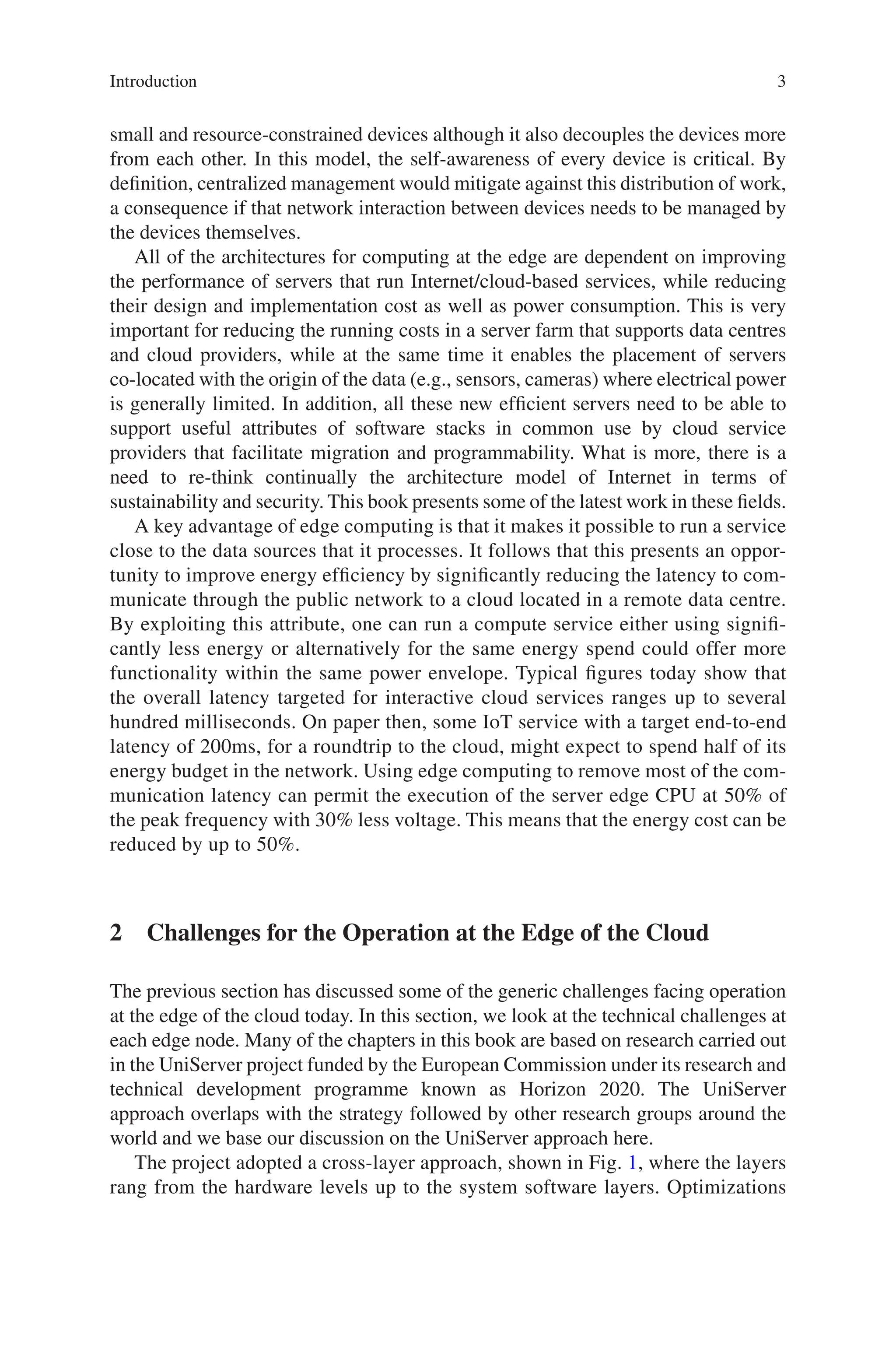
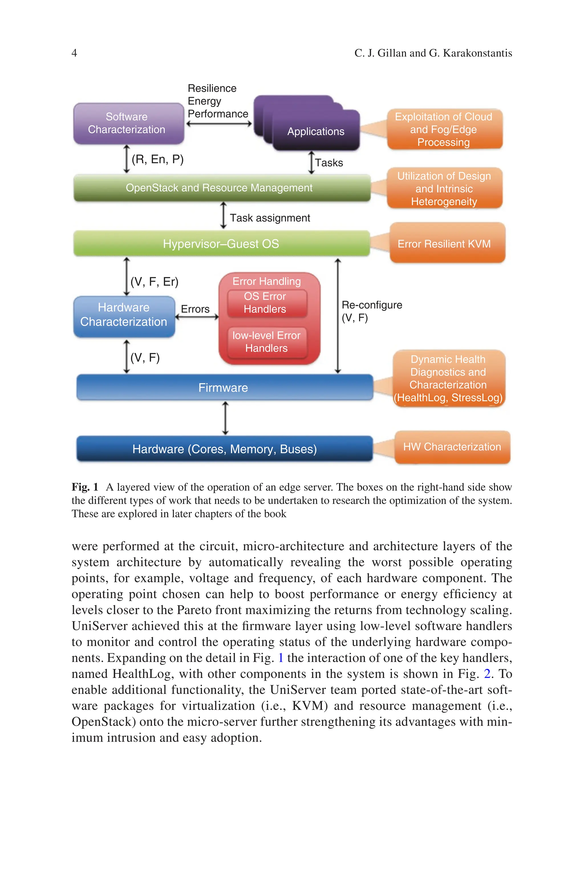
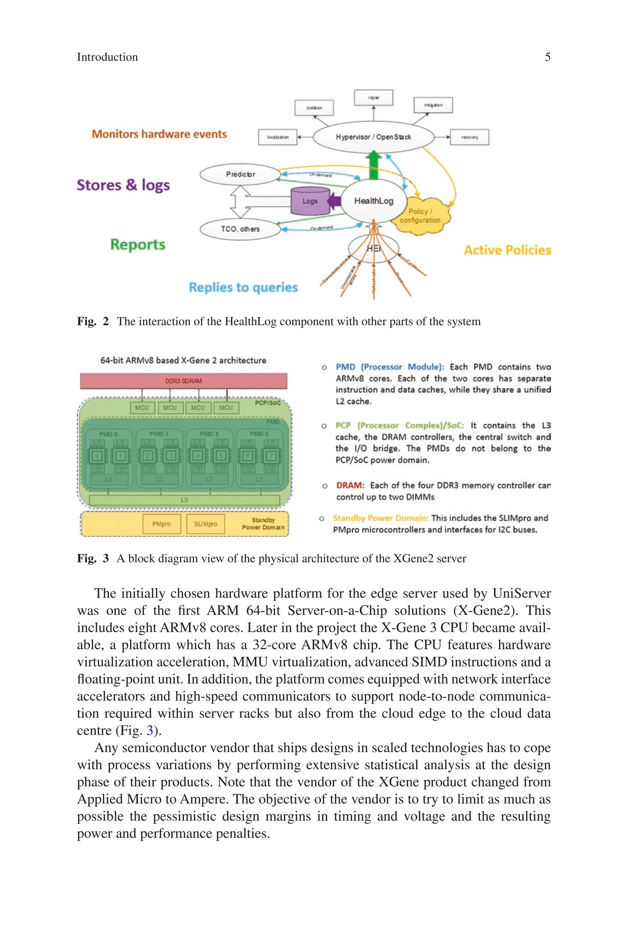
![6
2.1
Challenges for the operation of CPUs at the Edge
of the Cloud
Rather than trying to predict the operational margins at design time, an alternative
approach is to reveal these and to them effectively at the run-time on the actual
boards shipped to users. Figure 4 illustrates that this method takes account of
different types of operational changes inherent in CPU chips. The graph on the left-
hand side of the figure illustrates the distribution of operational frequency of chips
at the fabrication stage. Typically, the vendor will discard chips to the left or right of
the blue peak. The variation arises during chip fabrication due to small variances in
transistor dimensions (length, width, oxide thickness). These in turn have a direct
impact on the threshold voltage for the device. Other variations exist, some of which
can be attributed to ageing when deployed. The right-hand side of the figure shows
that using technologies mentioned above and described in later chapters of this
book, the CPU chips labelled red and green can be deployed in products.
2.1.1
Stagnant Power Scaling.
For over four decades Mooreʼs law, coupled with Dennard scaling [19], ensured the
exponential performance increase in every process generation through device,
circuit, and architectural advances. Up to 2005, Dennard scaling meant increased
transistor density with constant power density. If Dennard scaling would have
continued, according to Kumey [20], by the year 2020 we would have approximately
40 times increase in energy efficiency compared to 2013. Unfortunately, Dennard
scaling has ended because of the slowdown of voltage scaling due to slower scaling
of leakage current as compared to area scaling. The scale of the issue is depicted in
Fig. 5, based on collected data [21, 22].
Fig. 4 Schematic illustration of the variation in operational parameters of the CPU chips
C. J. Gillan and G. Karakonstantis](https://image.slidesharecdn.com/23098776-250511125104-f114a86f/75/Computing-At-The-Edge-New-Challenges-For-Service-Provision-Georgios-Karakonstantis-16-2048.jpg)
![7
Fig. 5 Comparison of energy efficiency relation to 2013 (y-axis) for three cases. The grey line is
Dennard Scaling, the blue line is from the ITRS roadmap and the organ line is a conservative
estimate
The increasing gap between the energy efficiency gains that could be achieved
according to the ideal Dennard scaling is what actually achieved based on the ITRS
roadmap [22] and the actual conservative voltage scaling. The end of Dennard
scaling has changed the semiconductor industry dramatically. To continue the
proportional scaling of performance and exploit Mooreʼs law scaling, processor
designers have focused on building multicore systems and servicing multiple tasks
in parallel instead of building faster single cores. Even so, limited voltage scaling
increasingly results in having a larger fraction of a chip unusable, commonly
referred to as Dark Silicon [21]. Some industrial technologists have previously
warned in a number of talks that meeting very tight power budgets may bring the
limitation of activating only nine percent of available transistors at any point in
time [21].
2.1.2
Variations and Pessimistic Margins
The variability in device and circuit parameters whether on a processor core within
a system on chip (SoC) or on a CPU in an enterprise-level server adversely impacts
both energy efficiency and the performance of the system. Voltage values will vary
in time during the microprocessor operation because of workload changes on the
system and furthermore due to changes in the environment whether the system is
located. Voltage safety margins are added therefore to ensure correct operation.
Introduction](https://image.slidesharecdn.com/23098776-250511125104-f114a86f/75/Computing-At-The-Edge-New-Challenges-For-Service-Provision-Georgios-Karakonstantis-17-2048.jpg)
![8
Table 1 summarizes some of the main causes for safety margins and provides their
relative contribution to the up-scaling of the supply voltage Vdd.
The added safety voltage margins increase energy consumption and force opera-
tion at a higher voltage or lower frequency. They may also result in lower yield or
field returns if a part operates at higher power than its specification allows. The
voltage margins are becoming more prominent with area scaling and the use of
more cores per chip large voltage droops [23, 24] reliability issues at low voltages
(Vmin) [25], and core to core variations [26]. The scale of pessimism is also
observed on recently measured ARM processors revealing more than 30% timing
and voltage margins in 28nm [24, 27]. Note that these margins are only due to the
characterized voltage droops and have not considered the joint effect of other
variability sources.
Combined leakage and variations have elevated power as a prime design param-
eter. If we need to go faster, we need to find ways to become more power efficient.
All other things being equal, if one design uses less power than another, then it has
headroom to improve performance by using more resources or operating at a higher
frequency. Simply put, the more energy efficient a chip is, the more functionality
with higher utilization occurs and, naturally, it will service more tasks.
3
Summary of Chapters in the Book
Each subsection below presents a short summary of the information presented in
each chapter of the book.
3.1 Introduction
This, the present chapter, introduces the general ideas presented in more detail in
each chapter that follows.
Table 1 Reasons for addition
of safety margins
Reasons for margins Vdd Up-scaling
Voltage droops ~20%
Vmin ~15%
Core-to-core variations ~5%
C. J. Gillan and G. Karakonstantis](https://image.slidesharecdn.com/23098776-250511125104-f114a86f/75/Computing-At-The-Edge-New-Challenges-For-Service-Provision-Georgios-Karakonstantis-18-2048.jpg)
![13
Challenges on Unveiling Voltage Margins
from the Node to the Datacentre Level
George Papadimitriou and Dimitris Gizopoulos
1 Introduction
Technology scaling has enabled improvements in the three major design optimiza-
tion objectives: performance increase, power consumption reduction, and die cost
reduction, while system design has focused on bringing more functionality into
products at a lower cost. While today’s microprocessors are much faster and much
more versatile than their predecessors, they also consume significantly more
power [1].
To date, the approach has been to attempt to lower the voltage with each process
generation. But as the voltage is lowered, leakage current and energy increase, con-
tributing to a higher power. These high-power densities impair the reliability of
chips and life expectancy, increase cooling costs, and even raise environmental con-
cerns primarily due to the heavy deployment and use of large data centers. Power
problems also pose issues for smaller mobile devices with limited battery capacity.
While these devices could be implemented using faster microprocessors and larger
memories, their battery life would be further diminished. Improvements in micro-
processor technology will eventually come to a standstill without cost-effective
solutions to the power problem.
Power and energy are commonly defined as the work performed by a system.
Energy is the total amount of work performed by a system over some time, whereas
power is the rate at which the system performs the work. In formal terms,
P
W
T
= (1)
G. Papadimitriou (*) · D. Gizopoulos
Department of Informatics and Telecommunications, National and Kapodistrian
University of Athens, Athens, Greece
e-mail: georgepap@di.uoa.gr
© Springer Nature Switzerland AG 2022
G. Karakonstantis, C. J. Gillan (eds.), Computing at the EDGE,
https://doi.org/10.1007/978-3-030-74536-3_2](https://image.slidesharecdn.com/23098776-250511125104-f114a86f/75/Computing-At-The-Edge-New-Challenges-For-Service-Provision-Georgios-Karakonstantis-23-2048.jpg)
![14
E P T
= ∗ (2)
where P is power, E is energy, T is a specific time interval, and W is the total work
performed in that interval. Energy is measured in joules, while power is measured
in watts [1].
The relation of the power and energy of a microprocessor can be described by a
simple example: by halving the rate of the input clock, the power consumed by a
microprocessor can be reduced. If the microprocessor, however, takes twice as long
to run the same programs, the total energy consumed is the same. Whether power or
energy should be reduced depends on the context. Reducing energy is often more
critical in data centers because they occupy an area of a few football fields, contain
tens of thousands of servers, consume electricity of small cities, and utilize expen-
sive cooling mechanisms.
There are two forms of power consumption: dynamic power consumption and
static power consumption. Dynamic power consumption is caused by circuit activ-
ity such as input changes in an adder or values in a register. As the following equa-
tion shows, the dynamic power (Pdynamic) depends on four parameters namely, supply
voltage (Vdd), clock frequency (f), physical capacitance (C), and an activity factor
(a) that relate to how many transitions occur in a chip:
P aCV f
dynamic = 2
(3)
Both static and dynamic variations lead microprocessor architects to apply con-
servative guardbands (operating voltage and frequency settings) to avoid timing
failures and guarantee correct operation, even in the worst-case conditions excited
by unknown workloads or the operating environment. Revealing and harnessing
the pessimistic design-time voltage margins offers a significant opportunity for
energy-
efficient computing in multicore CPUs. The full energy savings potential
can be exposed only when accurate core-to-core, chip-to-chip, and workload-to-
workload voltage scaling variation is measured. When all these levels of variation
are identified, system software can effectively allocate hardware resources to soft-
ware tasks matching the capabilities of the former (undervolting potential of the
CPU cores) and the requirements of the latter (for reduced energy or increased
performance).
In this chapter, we begin by briefly reviewing the currently established tech-
niques, which contribute to either unveil the pessimistic voltage margins or pro-
pose mitigation techniques to make the microprocessors more tolerant to
low-voltage conditions. Later, we describe the challenges in characterizing micro-
processor chips and present comprehensive solutions that overcome these chal-
lenges and can reveal the pessimistic voltage margins to unlock the full potential
energy savings.
G. Papadimitriou and D. Gizopoulos](https://image.slidesharecdn.com/23098776-250511125104-f114a86f/75/Computing-At-The-Edge-New-Challenges-For-Service-Provision-Georgios-Karakonstantis-24-2048.jpg)
![15
2
Supply Voltage Scaling: Challenges
and Established Techniques
2.1 Established Techniques
During the last years, the goal for improving microprocessors’ energy efficiency,
while reducing their power supply voltage, is a major concern of many scientific
studies that investigate the chips’ operation limits in nominal and off-nominal con-
ditions [2, 3]. In this section, we briefly summarize the existing studies and findings
concerning low-voltage operation and characterization studies.
Wilkerson et al. [4] go through the physical effects of low-voltage supply on
SRAM cells and the types of failures that may occur. After describing how each cell
has a minimum operating voltage, they demonstrate how typical error protection
solutions start failing far earlier than a low-voltage target (set to 500 mV) and pro-
pose two architectural schemes for cache memories that allow operation below
500 mV. The word-disable and bit-fix schemes sacrifice cache capacity to tolerate
the high failure rates of low voltage operation. While both schemes use the entire
cache on high voltage, they sacrifice 50% and 25% accordingly in 500 mV. Compared
to existing techniques, the two schemes allow a 40% voltage reduction with power
savings of 85%.
Chishti et al. [5] propose an adaptive technique to increase the reliability of cache
memories, allowing high tolerance on multi-bit failures that appear on the low-
voltage operation. The technique sacrifices memory capacity to increase the error-
correction capabilities, but unlike previously proposed techniques, it also offers soft
and non-persistent error tolerance. Additionally, it does not require self-testing to
identify erratic cells in order to isolate them. The MS-ECC design can achieve a
30% supply voltage reduction with 71% power savings and allows configurable
ECC capacity by the operating system based on the desired reliability level.
Bacha et al. [6] present a new mechanism for the dynamic reduction of voltage
margins without reducing the operating frequency. The proposed mechanism does
not require additional hardware as it uses existing error correction mechanisms on the
chip. By reading their error correction reports, it manages to reduce the operating
voltage while keeping the system in safe operation conditions. It covers both core-to-
core and dynamic variability caused by the running workload. The proposed solution
was prototyped on an Intel Itanium 9560 processor and was tested using SPECjbb2005
and SPEC CPU2000-based workloads. The results report promising power savings
that range between 18% and 23%, with marginal performance overheads.
Bacha et al. [7] again rely on error correction mechanisms to reduce operating
voltage. Based on the observation that low-voltage errors are deterministic, the
paper proposes a hardware mechanism that continuously probes weak cache lines to
fine-tune the system’s supply voltage. Following an initial calibration test that
reveals the weak lines, the mechanism generates simple write-read requests to trig-
ger error correction and is capable to adapt to voltage noise as well. The proposed
mechanism was implemented as a proof-of-concept using dedicated firmware that
Challenges on Unveiling Voltage Margins from the Node to the Datacentre Level](https://image.slidesharecdn.com/23098776-250511125104-f114a86f/75/Computing-At-The-Edge-New-Challenges-For-Service-Provision-Georgios-Karakonstantis-25-2048.jpg)
![16
resembles the hardware operation on an Itanium-based server. The solution reports
an average of 18% supply voltage reduction and an average of 33% power con-
sumption savings, using a mixed set of applications.
Bacha et al. [8] exploit the observation of deterministic error distribution to pro-
vide physically unclonable functions (PUF) to support security applications. They
use the error distribution of the lowest save voltage supply as an unclonable finger-
print, without the typical requirement of additional dedicated hardware for this pur-
pose. The proposed PUF design offers a low-cost solution for existing processors.
The design is reported to be highly tolerant to environmental noise (up to 142%)
while maintaining very small misidentification rates (below 1 ppm). The design was
tested on a real system using an Itanium processor as well as on simulations. While
this study serves a different domain, it highlights the deterministic error behavior on
SRAM cells.
Duwe et al. [9] propose an error-pattern transformation scheme that re-arranges
erratic bit cells that correspond to uncorrectable error patterns (e.g., beyond the cor-
rectable capacity) to correctable error patterns. The proposed method is low-latency
and allows the supply voltage to be scaled further than it was previously possible.
The adaptive rearranging is guided using the fault patterns detected by the self-test.
The proposed methodology can reduce the power consumption up to 25.7%, based
on simulated modeling that relies on literature SRAM failure probabilities.
There are several papers that explore methods to eliminate the effects of voltage
noise. Voltage noise can significantly increase the pessimistic voltage margins of the
microprocessor. Gupta et al. [10] and Reddi et al. [11] focus on the prediction of
critical parts of benchmarks, in which large voltage noise glitches are likely to
occur, leading to malfunctions. In the same context, several studies were presented
to mitigate the effects of voltage noise [12–14] [15, 16] or to recover from them
after their occurrence [17]. For example, in [18–20] the authors propose methods to
maximize voltage droops in single-core and multicore chips in order to investigate
their worst-case behavior due to the generated voltage noise effects.
Similarly, authors in [21, 22] proposed a novel methodology for generating di/dt
viruses that is based on maximizing the CPU emitted electromagnetic (EM) emana-
tions. Particularly, they have shown that a genetic algorithm (GA) optimization
search for instruction sequences that maximize EM emanations and generates a di/
dt virus that maximizes voltage noise. They have also successfully applied this
approach on 3 different CPUs: two ARM-based mobile CPUs and one AMD
Desktop CPU [23, 24].
Lefurgy et al. [25] propose the adaptive guardbanding in IBM Power 7 CPU. It
relies on the critical path monitor (CPM) to detect the timing margin. It uses a fast
CPM-DPLL (digital phase lock loop) control loop to avoid possible timing failures:
when the detected margin is low, the fast loop quickly stretches the clock. To miti-
gate the possible frequency loss, adaptive guardbanding also uses a slow loop to
boost the voltage when the averaged clock frequency is below the target. Leng et al.
[26] study the voltage guardband on the real GPU and show the majority of GPU
voltage margin protects against voltage noise. To fulfill the energy saving in the
guardband, the authors propose to manage the GPU voltage margin at the kernel
G. Papadimitriou and D. Gizopoulos](https://image.slidesharecdn.com/23098776-250511125104-f114a86f/75/Computing-At-The-Edge-New-Challenges-For-Service-Provision-Georgios-Karakonstantis-26-2048.jpg)
![17
granularity. They study the feasibility of using a kernel’s performance counters to
predict the Vmin, which enables a simpler predictive guardbanding design for GPU-
like co-processors.
Aggressive voltage underscaling has been recently applied in part to FPGAs, as
well. Ahmed et al. [27] extend a previously proposed offline calibration-based DVS
approach to enable DVS for FPGAs with BRAMs using a testing circuitry to ensure
that all used BRAM cells operate safely while scaling the supply voltage. L. Shen
et al. [28] propose a DVS technique for FPGAs with Fmax; however, voltage under-
scaling below the safe level is not thoroughly investigated. Ahmed et al. [29] evalu-
ate and compare the voltage behavior of different FPGA components such as LUTs
and routing resources and design FPGA circuitry that is better suited for voltage
scaling. Salamat et al. [30] evaluate at simulation level a couple of FPGA-based
DNN accelerators with low-voltage operations.
As we can see, several microarchitectural techniques have been proposed that
eliminate a subset of these guardbands for efficiency gains over and above what is
dictated by the design conservative guardbands. However, all of these techniques
are associated with significant design, test, and measurement overheads that limit its
application in the general case. Another example is the Razor technique [31], sup-
port for timing-error detection and correction has to be explicitly designed into the
processor microarchitecture which comes with significant verification overheads
and circuit costs. Similarly, in adaptive-clocking approaches [32], extensive test and
verification effort is required until the microprocessor is released to the market.
Ensuring the eventual success of these techniques requires a deep understanding of
dynamic margins and their manifestation during normal code execution.
2.2 Supply Voltage Scaling
Reducing supply voltage is one of the most efficient techniques to reduce the
dynamic power consumption of the microprocessor, because dynamic power is qua-
dratic in voltage (as Eq. 3 shows). However, supply voltage scaling increases sub-
threshold leakage currents, increases leakage power, and also poses numerous
circuit design challenges. Process variations and temperature parameters (dynamic
variations), caused by different workload interactions, are also major factors that
affect microprocessor’s energy efficiency. Furthermore, during microprocessor chip
fabrication, process variations can affect transistor dimensions (length, width, oxide
thickness, etc. [33]) which have direct impact on the threshold voltage of a MOS
device [34].
As technology scales further down, the percentage of these variations compared
to the overall transistor size increases and raises major concerns for designers, who
aim to improve energy efficiency. This variation is classified as static variation and
remains constant after fabrication. Both static and dynamic variations lead micro-
processor architects to apply conservative guardbands (operating voltage and fre-
quency settings), as shown in Fig. 1a to avoid timing failures and guarantee correct
Challenges on Unveiling Voltage Margins from the Node to the Datacentre Level](https://image.slidesharecdn.com/23098776-250511125104-f114a86f/75/Computing-At-The-Edge-New-Challenges-For-Service-Provision-Georgios-Karakonstantis-27-2048.jpg)
![18
operation, even in the worst-case conditions excited by unknown workloads, envi-
ronmental conditions, and aging [35, 36]. The guardband results in faster circuit
operation under typical workloads than required at the target frequency, resulting in
additional cycle time, as shown in Fig. 1b. In case of a timing emergency caused by
voltage droops, the extra margin prevents timing violations and failures by tolerat-
ing circuit slowdown. While static guardbanding ensures robust execution, it tends
to be severely overestimated as timing emergencies rarely occur, making it less
energy-efficient [32]. These pessimistic guardbands impede power consumption
and performance, and block the savings that can be derived by reducing the supply
voltage (Fig. 1c) and increasing the operation frequency, respectively, when condi-
tions permit.
2.3
System-Level Characterization Challenges
To bridge the gap between energy efficiency and performance improvements, sev-
eral hardware and software techniques have been proposed, such as Dynamic
Voltage and Frequency Scaling (DVFS) [37]. The premise of DVFS is that a micro-
processor’s workloads as well as the cores’ activity vary, so when one or more cores
have less or no work to perform, the frequency, and thus, the voltage can be slowed
down without affecting performance adversely. However, to further reduce the
power consumption by keeping the frequency high when it is necessary, recent stud-
ies aim to uncover the conservative operational limits, by performing an extensive
system-level voltage scaling characterization of commercial microprocessors’ oper-
ation beyond nominal conditions [38] [39] [40–42]. These studies leverage the
Reliability, Accessibility, and Serviceability (RAS) features, provided by the hard-
ware (such as ECC), in order to expose reduced but safe operating margins.
A major challenge, however, in voltage scaling characterization at the system
level is the time-consuming large population of experiments due to: (i) different
voltage and frequency levels, (ii) different characterization setups (e.g., for a
Cycle Time
Timing Margin
Nominal
Voltage
Guardband
Actual
Needed
Voltage
Nominal
Static
Margin
Reduced
Voltage
Margin
(a) Guardband (b) Static Margin (c) Reduced Voltage Margin
Fig. 1 Voltage guardband ensures reliability by inserting an extra timing margin. Reduced voltage
margins improve total system efficiency without affecting the reliability of the microprocessor
G. Papadimitriou and D. Gizopoulos](https://image.slidesharecdn.com/23098776-250511125104-f114a86f/75/Computing-At-The-Edge-New-Challenges-For-Service-Provision-Georgios-Karakonstantis-28-2048.jpg)
![20
ensure the credibility of the delivered results because when a system operates
beyond nominal conditions it can fall into unstable states. In the next section, we
describe a fully automated characterization framework [43, 44], which can over-
come the above challenges and result in correct and reliable findings, which may be
used as a basis for any further energy-efficient technique.
3
Automated Characterization Framework
The primary goals of the described framework are: (1) to identify the target system’s
limits when it operates at underscaled voltage and frequency conditions, and (2) to
record/log the effects of a program’s execution under these conditions. The frame-
work should provide at least the following features:
• Comparing the outcome of the program with the correct output of the program
when the system operates in nominal conditions to record Silent Data
Corruptions (SDCs).
• Monitoring the exposed corrected and uncorrected errors from the hardware plat-
form’s error reporting mechanisms.
• Recognizing when the system is unresponsive to restore it automatically.
• Monitoring system failures (crash reports, kernel hangs, etc.).
• Determining the safe, unsafe, and non-operating voltage regions for each appli-
cation for all available clock frequencies.
• Performing massive repeated executions of the same configuration.
The automated framework (outlined in Fig. 2) is easily configurable by the user,
can be embedded to any Linux-based system, with similar voltage and frequency
regulation capabilities, and can be used for any voltage and frequency scaling char-
acterization study.
To completely automate the characterization process, and due to the frequent and
unavoidable system crashes that occur when the system operates in reduced voltage
levels, a Raspberry Pi board is connected externally to the system board, which
behaves as a watchdog. The Raspberry is physically connected to both the Serial
Port and the Power and Reset buttons of the system board to enable physical access
to the system.
3.1 Initialization Phase
During the initialization phase, a user can define a list of benchmarks with any input
dataset to run in any desirable characterization setup. The characterization setup
includes the voltage and frequency (V/F) values under which the experiment will
take place and the cores where the benchmark will be run; this can be an individual
core, a pair of cores, or all of the available eight cores in the microprocessor. The
G. Papadimitriou and D. Gizopoulos](https://image.slidesharecdn.com/23098776-250511125104-f114a86f/75/Computing-At-The-Edge-New-Challenges-For-Service-Provision-Georgios-Karakonstantis-30-2048.jpg)
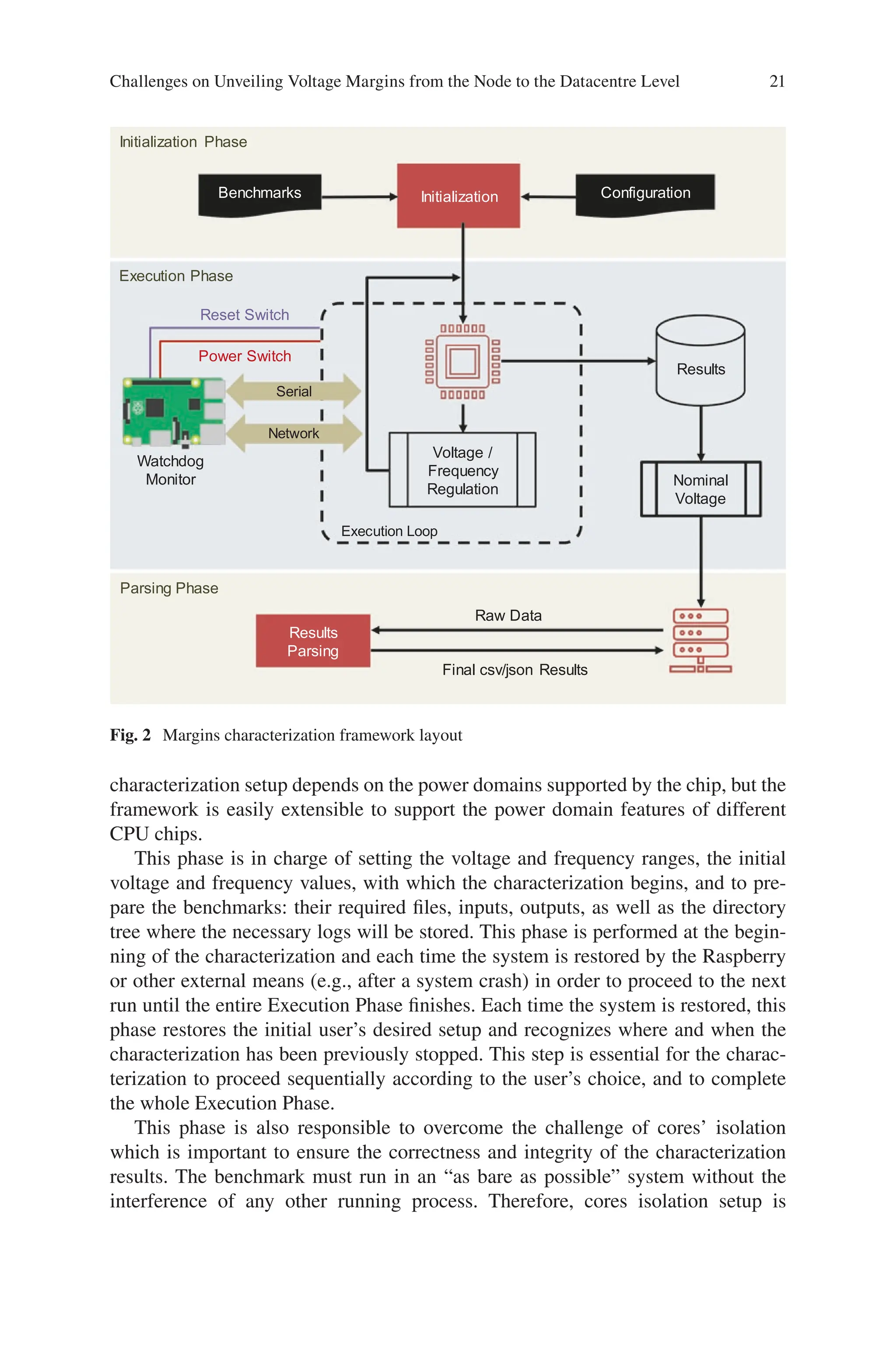
![22
twofold: first, it recognizes these cores or group of cores that are not currently under
characterization, and migrates all currently running processes (except for the bench-
mark) to a completely different core. The migration of system processes is required
to isolate the execution of the desired benchmark from all other active processes.
Second, given that more than one cores in the majority of current microproces-
sors are in the same power domain, they always have the same voltage value (in case
this does not hold in a different microarchitecture the described framework can be
adapted). This means that even though there are several processes run on different
cores (not in the core(s) under characterization), they have the same probability to
affect an unreliable operation while reducing the voltage. On the other hand, each
individual core (or pair of cores) can have a different clock frequency, so we lever-
age the combination of V/F states in order to set the core under characterization to
the desired frequency, and all other cores to the minimum available frequency in
order to ensure that an unreliable operation is due to the benchmark’s execution
only. When for example the characterization takes place in the cores 0 and 1, they
set to the pre-defined by the user frequency (e.g., the maximum frequency), and all
the other available cores are set to the minimum available frequency. Thus, all the
running processes, except for the benchmark, are executed isolated.
3.2 Execution Phase
After the characterization setup is defined, the automated Execution Phase begins.
The Execution Phase consists of multiple runs of the same benchmark, each one
representing the execution of the benchmark with a pre-defined characterization
setup. The set of all the characterization runs running the same benchmark with dif-
ferent characterization setups represents a campaign. After the initialization phase,
the framework enters the Execution Phase, in which all runs take place. The runs are
executed according to the user’s configuration, while the framework reduces the
voltage with a step defined by the user in the initialization phase. For each run, the
framework collects and stores the necessary logs at a safe place externally to the
system under characterization, which will be then used by the parsing phase.
The logged information includes: the output of the benchmark at each execution,
the corrected and uncorrected errors (if any) collected by the Linux EDAC Driver
[45], as well as the errors’ localization (L1, L2, L3 cache, DRAM, etc.), and several
failures, such as benchmark crash, kernel hangs, and system unresponsiveness. The
framework can distinguish these types of failures and keep logging about them to be
parsed later by the parsing phase. Benchmark crashes can be distinguished by moni-
toring the benchmark’s exit status. On the other hand, to identify the kernel hangs
and system unresponsiveness, during this phase the framework notifies the Raspberry
when the execution is about to start and also when the execution finishes.
In the meantime, the Raspberry starts pinging the system to check its responsive-
ness. If the Raspberry does not receive a completion notification (hang) in the given
time (we defined as timeout condition 2 times the normal execution time of the
G. Papadimitriou and D. Gizopoulos](https://image.slidesharecdn.com/23098776-250511125104-f114a86f/75/Computing-At-The-Edge-New-Challenges-For-Service-Provision-Georgios-Karakonstantis-32-2048.jpg)
![23
benchmark) or the system turns completely unresponsive (ping is not responding),
the Raspberry sends a signal to the Power Off button on the board, and the system
resets. After that, the Raspberry is also responsible to check when the system is up
again, and sends a signal to restart the experiments. These decisions contribute to
the Failure Recognition challenge.
During the experiments, some Linux tasks or the kernel may hang. To identify
these cases, we use an inherent feature of the Linux kernel to periodically detect
these tasks by enabling the flag “hung_task_panic” [45]. Therefore, if the kernel
itself recognizes a process hang, it will immediately reset the system, so there is no
need for the Raspberry to wait until the timeout. In this way, we also contribute to
the Failure Recognition challenge and accelerate the reset procedure and the entire
characterization.
Note that, in order to isolate the framework’s execution from the core(s) under
characterization, the operations of the framework are also performed in isolation (as
described previously). However, when there are operations of the framework, such
as the organization of log files during the benchmark’s execution that is an integral
part of the framework, and thus, they must run in the core(s) under characterization,
these operations are performed after the benchmark’s execution in the nominal con-
ditions. This is the way to ensure that any logging information will be stored cor-
rectly and no information will be lost or changed due to the unstable system
conditions, and thus, to overcome the Safe Data Collection challenge.
3.3 Parsing Phase
In the last step of the framework, all the log files that are stored during the Execution
Phase are parsed in order to provide a fine-grained classification of the effects
observed for each characterization run. Note that, each run is correlated to a specific
benchmark and characterization setup. The categories that are used for our classifi-
cation are summarized in Table 1, but the parser can be easily extended according to
the user’s needs. For instance, the parser can also report the exact location that the
correctable errors occurred (e.g., the cache level, the memory, etc.) using the log-
ging information provided by the Execution Phase.
Note that each characterization run can manifest multiple effects. For instance,
in a run both SDC and CE can be observed; thus, both of them should be reported
by the parser for this run. Furthermore, the parser can report all the information col-
lected during multiple campaigns of the same benchmark. The characterization runs
with the same configuration setup of different campaigns may also have different
effects with different severity. For instance, let us assume two runs with the same
characterization setup of two different campaigns. After the parsing, the first run
finally revealed some CEs, and the second run was classified as SDC. At the end of
the parsing step, all the collected results concerning the characterization (according
to Table 1) are reported in .csv and .json files.
Challenges on Unveiling Voltage Margins from the Node to the Datacentre Level](https://image.slidesharecdn.com/23098776-250511125104-f114a86f/75/Computing-At-The-Edge-New-Challenges-For-Service-Provision-Georgios-Karakonstantis-33-2048.jpg)
![24
Table 1 Experimental effect categorization
Effect Description
ΝΟ
(Normal Operation)
The benchmark was successfully completed without any
indications of failure.
SDC
(Silent Data Corruption)
The benchmark was successfully completed, but a mismatch
between the program output and the correct output was observed.
CE
(Corrected Error)
Errors were detected and corrected by the hardware.
UE
(Uncorrected Error)
Errors were detected, but not corrected by the hardware.
AC
(Application Crash)
The application process was not terminated normally (the exit
value of the process was different than zero).
TO
(Application Timeout)
The application process cannot finish and exceeds its normal
execution time (e.g., infinite loop).
SC
(System Crash)
The system was unresponsive; meaning that the X-Gene 2 is not
responding to pings or the timeout limit was reached.
4
Fast System-Level Voltage Margins Characterization
Apart from the automated characterizing framework, which overcomes the previ-
ously described challenges, there is also one more important challenge when char-
acterizing the pessimistic voltage margins. The characterization procedure to
identify these margins becomes more and more difficult and time-consuming in
modern multicore microprocessor chips, as the systems become more complex and
non-deterministic and the number of cores is rapidly increasing [46–54]. In a mul-
ticore CPU design, there are significant opportunities for energy savings, because
the variability of the safe margins is large among the cores of a chip, among the
different workloads that can be executed on different cores of the same chip and
among the chips of the same type.
The accurate identification of these limits in a real multicore system requires
massive execution of a large number of real workloads (as we have seen in the pre-
vious sections) in all the cores of the chip (and all different chips of a system), for
different voltage and frequency values. The excessively long time that SPEC-
based
or similar characterization takes forces manufacturers to introduce the same pessi-
mistic guardband for all the cores of the same multicore chips. Clearly, if shorter
benchmarks are able to reveal the Vmin of each core of a multicore chip (or the Vmin
of different chips) faster than exhaustive campaigns, finer-grained exploitation of
the operational limits of the chips and their cores can be effectively employed for
energy-efficient execution of the workloads.
In this section, we introduce the development of dedicated programs (diagnostic
micro-viruses), which are presented in [55]. Micro-viruses aim to stress the funda-
mental hardware components of a microprocessor and unveil the pessimistic volt-
age margins significantly faster rather than running extensive campaigns using
long-time and diverse benchmarks.
G. Papadimitriou and D. Gizopoulos](https://image.slidesharecdn.com/23098776-250511125104-f114a86f/75/Computing-At-The-Edge-New-Challenges-For-Service-Provision-Georgios-Karakonstantis-34-2048.jpg)
![25
With diagnostic micro-viruses, one can effectively stress (individually or simul-
taneously) all the main components of the microprocessor chip:
(a) The caches (the L1 data and instruction caches, the unified L2 caches, and the
last level L3 cache of the chips).
(b) The two main functional components of the pipeline (the ALU and the FPU).
These diagnostic micro-viruses are executed in a very short time (~3 days for the
entire massive characterization campaign for each individual core for each one
microprocessor chip) compared to normal benchmarks such as those of the SPEC
CPU2006 suite which need 2 months as Fig. 3a shows.
The micro-viruses’ purpose is to reveal the variation of the safe voltage margins
across cores of the multicore chip and also to contribute to diagnosis by exposing
and classifying the abnormal behavior of each CPU unit (silent data corruptions,
bit-cell errors, and timing failures).
There have been many efforts toward writing power viruses and stress bench-
marks. For example, SYMPO [56], an automatic system-level max power virus gen-
eration framework, which maximizes the power consumption of the CPU and the
memory system, MAMPO [57], as well as the MPrime [58] and stress-ng [59] are
the most popular benchmarks, which aim to increase the power consumption of the
microprocessor by torturing it; they have been used for testing the stability of the
microprocessor during overclocking. However, power viruses are not capable to
reveal pessimistic voltage margins.
Figure 3b shows that the power consumption of a workload is not correlated to
the safe Vmin (and thus to voltage guardbands) of a core. As we can see, libquantum
is the most power-hungry benchmark among the 12 SPEC CPU2006 benchmarks
we used. However, libquantum’s safe Vmin is significantly lower (20 mV) than the
namd benchmark, which has lower power consumption.
The purpose of the micro-viruses is to stress individually the fundamental micro-
processor units (caches, ALU, FPU) that define the voltage margins variability of
the microprocessor. Micro-viruses do not aim to reveal the absolute Vmin (which can
be identified by worst-case voltage noise stress programs). However, we provide
37.6
20.7
1.5 1.9
0
10
20
30
40
50
60
70
1T 8T
Days
(a)
SPEC Micro-Viruses
870
880
890
900
910
920
0
4
8
12
16
libquantum namd Viruses
Vmin
(mV)
Power
(Watt)
(b)
Power Vmin
Fig. 3 (a) Time needed for a complete system-level characterization to reveal the pessimistic
margins for one chip. Programs are executed on individual cores (1 T) and on all 8 cores concur-
rently (8 T). (b) Safe Vmin values and their independence on power consumption
Challenges on Unveiling Voltage Margins from the Node to the Datacentre Level](https://image.slidesharecdn.com/23098776-250511125104-f114a86f/75/Computing-At-The-Edge-New-Challenges-For-Service-Provision-Georgios-Karakonstantis-35-2048.jpg)
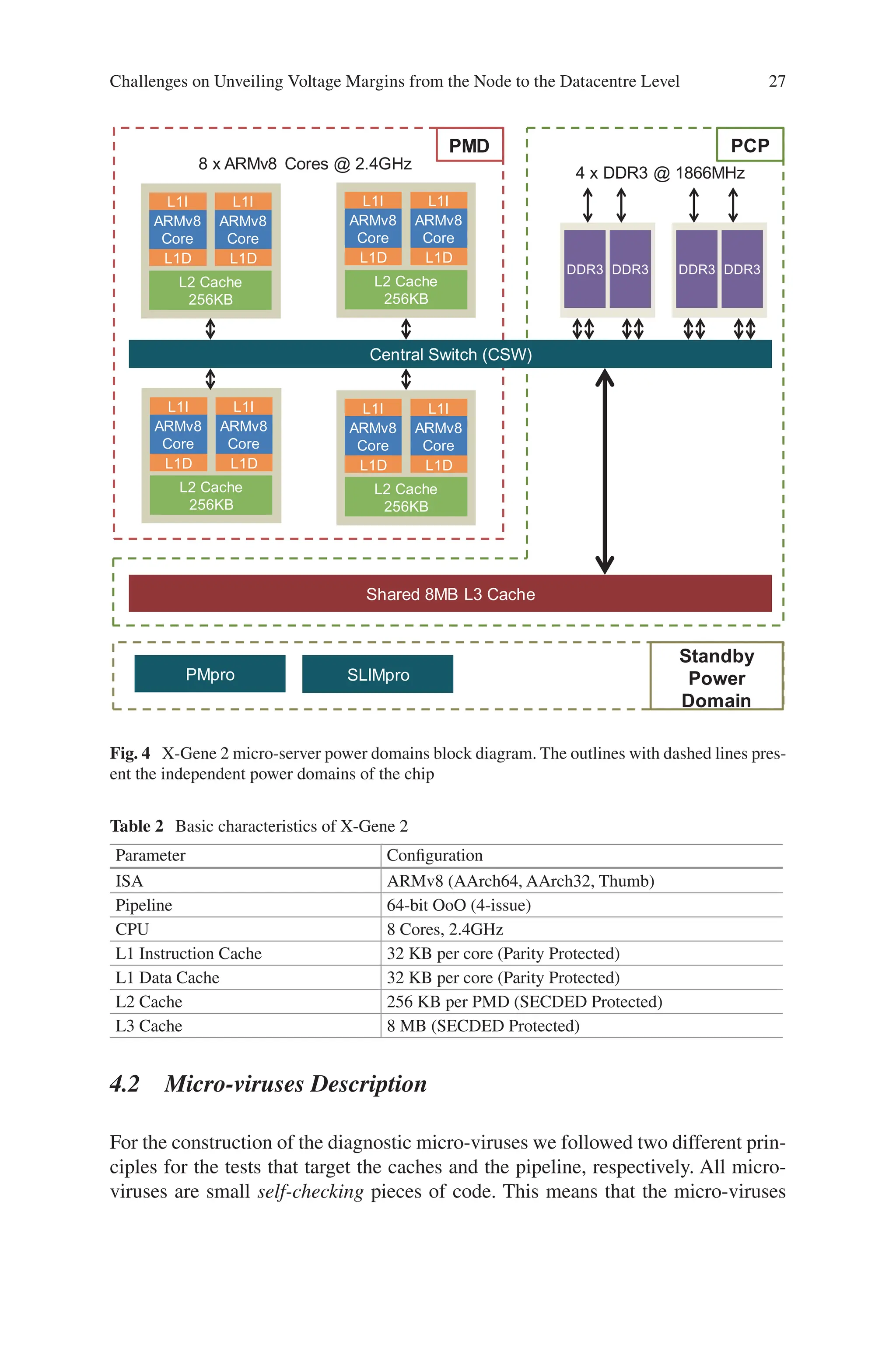
![28
Table 3 The X-Gene 2 cache specifications
L1I L1D L2 L3
Size 32 KB 32 KB 256 KB 8 MB
# of Ways 8 8 32 32
Block Size 64 B 64 B 64 B 64 B
# of Blocks 512 512 4096 131,072
# of Sets 64 64 128 4096
Write Policy – Write-through Write-Back –
Write Miss
Policy
No-write allocate No-write allocate Write allocate –
Organization Physically
Indexed
Physically Tagged
(PIPT)
Physically
Indexed
Physically Tagged
(PIPT)
Physically
Indexed
Physically Tagged
(PIPT)
Physically
Indexed
Physically Tagged
(PIPT)
Prefetcher YES YES YES NO
Scope Per Core Per Core Per PMD Shared
Protection Parity Protected Parity Protected ECC Protected ECC Protected
check if a read value is the expected one or not. There are previous studies (e.g., [60,
61]) for the construction of such tests, but they focus only on error detection (mainly
for permanent errors), and to our knowledge this is the first study that is performed
on actual microprocessor chips; not in simulators or RTL level, which have no inter-
ference with the operating system and the corresponding challenges.
In this section, we first present the details of the caches of the X-Gene 2 in
Table 3 (the rest of important X-Gene 2’s specifications were discussed previously)
and then a brief overview of the challenges for the development of such system-
level micro-viruses in a real hardware and the decisions we made in order to develop
accurate self-checking tests for the caches and the pipeline.
Caches For all levels of caches the first goal of the developed micro-viruses is to
flip all the bits of each cache block from zero to one and vice versa. When the cache
array is completely filled with the desired data, the micro-virus reads iteratively all
the cache blocks while the chip operates in reduced voltage conditions and identifies
any corruptions of the written values, which cannot be detected by dedicated hard-
ware mechanisms of the cache, such as the parity protection that can detect only odd
number of flips.
All caches in X-Gene 2 have pseudo-LRU replacement policy. All our micro-
viruses focusing on any cache level need to “warm-up” the cache before the test
begins, by iteratively accessing the desired data in order to ensure that all the ways
of the cache are completely filled and accessed with the micro-viruses’ desired pat-
terns. We experimentally observed through the performance monitoring counters
that the safe number of iterations that “warm-up” the cache with the desired data,
before the checking phase begins, is log2(number of ways) to guarantee that the
cache is filled only with the data of the diagnostic micro-virus.
G. Papadimitriou and D. Gizopoulos](https://image.slidesharecdn.com/23098776-250511125104-f114a86f/75/Computing-At-The-Edge-New-Challenges-For-Service-Provision-Georgios-Karakonstantis-38-2048.jpg)
![29
In order to validate the operation of the entire cache array, it is important to per-
form write/read operations in all bit cells. For every cache level, we allocate a mem-
ory chunk equal to the targeted cache size. As the storing of data is performed in
cache block granularity, we need to make sure that our data storage is block-aligned,
otherwise we will encounter undesirable block replacements that will break the
requirement for complete utilization of the cache array.
Assume for example that the first word of the physical frame will be placed at
the middle of the cache block. This means that when the micro-virus fills the
cache, practically, there will be half-block size words that will replace a desired
previously fetched block in the cache. Thus, if the cache blocks are N, the number
of blocks that will be written in the cache will be N +1 (which means that one
cache block will get replaced), and thus, the self-checking property may be jeop-
ardized. To this end, for all cache-related micro-viruses we perform a check at the
beginning of the test to guarantee that the allocated array is cache aligned (to be
block aligned afterward).
Another factor that has to be considered in order to achieve full coverage of the
cache array is the cache coloring [62]. Unless the memory is a fully associative one
(which is not the case of the ARMv8 microprocessors), every store operation is
indexed at one cache block depending on its address. For physically indexed memo-
ries, the physical address of the datum or instruction is used. However, because the
physical addresses are not known or accessible from the software layer, special
precautions need to be taken in order to avoid unnecessary replacements. To address
this issue, we exploit a technique that is used to improve cache performance, known
as cache coloring [62]. If the indexing range of the memory is larger than the virtual
page, two addresses with the same offset on different virtual pages are likely to
conflict on the same cache block (due to the 32 KB size of the L1 caches the bits that
index the cache occur in page offset, and thus, there is no conflict; this is the case for
L2 and L3 caches in our system). To avoid this situation, the indexing range is sepa-
rated in regions equal to the page size, known as colors. It is then enough to use an
equal number of pages in each color to avoid conflicts. The easiest way to achieve
this is to allocate contiguous physical address range, which is possible at the kernel
level using the kmalloc() call. The contiguous physical range will guarantee that all
the data will be placed and fully occupy the cache, without replacements or unoc-
cupied blocks.
Another challenge that the micro-viruses need to take into consideration is the
interference of the branch predictors and the cache prefetchers. In our micro-viruses,
the branch prediction mechanism (in particular the branch mispredictions that can
flush the entire pipeline) may ruin the self-checking property of the micro-virus, by
replacing or invalidating the necessary data or instruction patterns. Moreover,
prefetching requests can modify the pre-defined access patterns of the micro-virus
execution.
To eliminate these effects, the memory access patterns of the micro-viruses are
modeled using the stride-based model for each of the static loads and stores of the
Challenges on Unveiling Voltage Margins from the Node to the Datacentre Level](https://image.slidesharecdn.com/23098776-250511125104-f114a86f/75/Computing-At-The-Edge-New-Challenges-For-Service-Provision-Georgios-Karakonstantis-39-2048.jpg)
![31
(three consecutive times) before the test begins, in order to ensure that all the blocks
with the desired patterns are allocated in the first level data cache. With these steps,
we achieve 100% read hit in the L1 data cache during the execution of the L1D
micro-virus in undervolted conditions. The L1 data micro-virus fills the L1 data
cache with three different patterns, each of which corresponds to a different micro-
virus test. These tests are the all-zeros, the all-ones, and the checkerboard pattern.
To enable the self-checking property of the micro-virus (correctness of execution is
determined by the micro-virus itself and not externally), at the end of the test we
check if each fetched word is equal to the expected value (the one stored before the
test begins).
4.2.2
L1 Instruction Cache Micro-virus
The concept behind the L1 instruction cache micro-virus is to flip all the bits of the
instruction encoding in the cache block from zero to one and vice versa. In the
ARMv8 ISA there is no single pair of instructions that can be employed to invert all
32 bits of an instruction word in the cache, so to achieve this we had to employ
multiple instructions. The instructions listed in Table 4 are able to flip all the bits in
the instruction cache from 0 to 1 and vice versa according to the Instruction
Encoding Section of the ARMv8 Manual [63].
Each cache block of the L1 instruction cache holds 16 instructions because each
instruction is 32-bit in ARMv8 and the L1 Instruction cache block size is 64 bytes.
The size of each way of the L1 instruction cache is 32 KB/8 = 4 KB, and thus, it is
equal to the page size which is 4 KB. As a result, there should be no conflict misses
when accessing a code segment (see cache coloring previously discussed) with size
equal to the L1 instruction cache (the same argument holds also for the L1
data cache).
The method that guarantees the self-checking property in the L1 Instruction
cache micro-virus is the following: The L1 instruction cache array holds 8192
instructions (64 sets x 8 ways x 16 instructions in each cache block = 8192). We use
8177 instructions to hold the instructions of our diagnostic micro-virus, and the
remaining 15 instructions (8177 + 15 = 8192) to compose the control logic of the
self-checking property and the loop control.
More specifically, we execute iteratively 8177 instructions and at the end of this
block of code, we expect the destination registers to hold a specific “signature” (the
signature is the same for each iteration of the same group of instructions, but differ-
ent among different executed instructions). If this “signature” is distorted, then the
micro-virus detects that an error occurred (for instance a bit flip in an immediate
instruction resulted in the addition of a different value) and records the location of
the faulty instruction as well as the expected and the faulty signature for further
diagnosis. We iterate this code multiple times and after that we continue with the
next block of code.
Challenges on Unveiling Voltage Margins from the Node to the Datacentre Level](https://image.slidesharecdn.com/23098776-250511125104-f114a86f/75/Computing-At-The-Edge-New-Challenges-For-Service-Provision-Georgios-Karakonstantis-41-2048.jpg)
![32
Table 4 ARMv8 instructions used in the L1I micro-virus. The right column presents the encoding
of each instruction to demonstrate that all cache block bits get flipped
Instruction Encoding
add x28, x28, #0x1 1001 0001 0000 0000 0000 0111 1001 1100
sub x3, x3, #0xffe 1101 0001 0011 1111 1111 1000 0110 0011
madd x28, x28, x27, x27 1001 1011 0001 1011 0110 1111 1001 1100
add x28, x28, x27, asr #2 1000 1011 1001 1011 0000 1011 1001 1100
add w28, w28,w27,lsr #2 0000 1011 0101 1011 0000 1011 1001 1100
nop 1101 0101 0000 0011 0010 0000 0001 1111
bics x28, x28, x27 1110 1010 0011 1011 0000 0011 1001 1100
As in the L1 data cache micro-virus, due to the pseudo-LRU policy that is used
also in the L1 Instruction cache, we fetch all the instructions.
log log .
2 2
1 8 3
number of ways of L Icache
( ) = ( ) =
(three consecutive times) before the test begins, to ensure that all blocks with the
desired instruction patterns are allocated in the L1 instruction cache. With these
steps, we achieve 100% cache read hit (and thus cache stressing) during undervolt-
ing campaigns.
4.2.3
L2 Cache Micro-virus
The L2 cache is a 32-way associative PIPT cache with 128 sets; thus, the bits of
the physical address that determine the block placement in the L2 cache are bits
[12:6] (as shown in Fig. 5). Moreover, the page size we rely on is 4 KB and con-
sequently the page offset consists of the 12 least significant bits of the physical
address. Accordingly, the most significant bit (bit 12) of the set index (the dotted
square in Fig. 5) is not a part of the page offset. If this bit is equal to 1, then the
block is placed in any set of the upper half of the cache, and in the same manner,
if this bit is equal to 0, the block is placed in a set of the lower half of the cache.
Bits [11:6] which are part of page/frame offset determine all the available sets for
each individual half.
In order to guarantee the maximum block coverage (e.g., to completely fill the
L2 cache array), and thus to fully stress the cache array, the L2 micro-virus should
not depend on the MMU translations that may result in increased conflict misses.
The way to achieve this is by allocating memory that is not only virtually contigu-
ous (as with the standard C memory allocation functions used in user space), but
also physically contiguous by using the kmalloc() function. The kmalloc() function
G. Papadimitriou and D. Gizopoulos](https://image.slidesharecdn.com/23098776-250511125104-f114a86f/75/Computing-At-The-Edge-New-Challenges-For-Service-Provision-Georgios-Karakonstantis-42-2048.jpg)
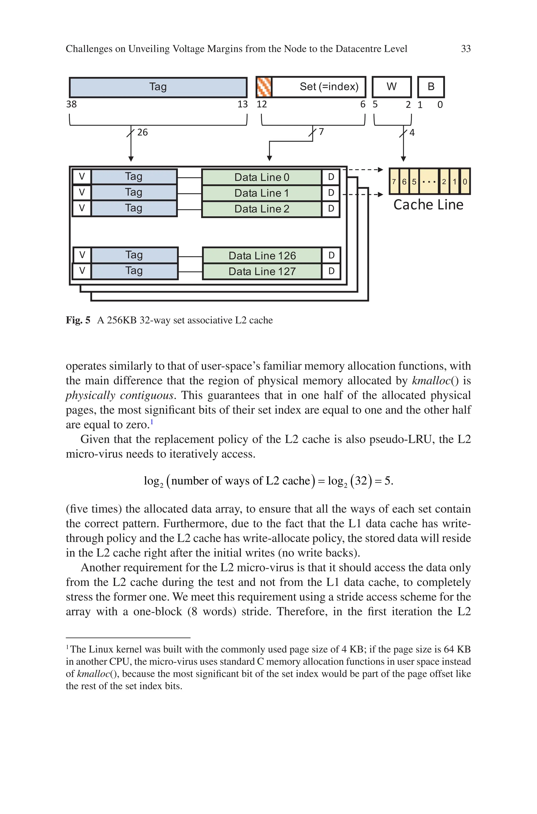
![34
micro-
virus accesses the first word of each block, in the second iteration it accesses
the second word of each block, and so on. Thus, it always misses the L1 data cache.
By accessing the data using these strides, the L2 micro-virus also overcomes the
prefetching requests. Note that the L1 instruction cache can completely hold all the
L2 diagnostic micro-virus instructions, so the L2 cache holds only the data of
our test.
To validate the above, we isolated all the system processes by forcing them to run
on different cores from the one that executes the L2 diagnostic micro-virus, by set-
ting the system processes’ CPU affinity and interrupts to a different core, and we
measured the L1 and L2 accesses and misses after we have already “trained” the
pseudo-LRU with the initial accesses. We measure these micro-architectural events
by leveraging the built-in performance counters of the CPU.
The performance counters show that the L2 diagnostic micro-virus always
misses the L1 data cache and always hits the L1 Instruction cache, while it hits the
L2 cache in the majority of the accesses. Specifically, the L2 cache has 4096 blocks
and the maximum number of block-misses we observed was 32 at most for each
execution of the test (meaning 99.2% coverage). In that way, we verify that the L2
micro-virus completely fills the L2 cache.
The L2 micro-virus fills the L2 cache with three different patterns, each of which
corresponds to a different micro-virus test. These tests are the all-zeros, the all-ones,
and the checkerboard pattern. To enable the self-checking property into this micro-
virus, at the end of the test we check if each fetched word is equal to the expected
value (the one stored before the test begins).
4.2.4
L3 Cache Micro-virus
The L3 cache is a 32-way associative PIPT cache with 4096 sets and is organized in
32 banks; so, each bank has 128 sets and 32 ways. Moreover, the bits of the physical
address that determine the block placement in the L3 cache are the bits [12:6] (for
choosing the set in a particular bank) and the bits [19:15] for choosing the correct
bank. Based on the above, in order to fill the L3 cache, we allocate physically con-
tiguous memory with kmalloc().
However, kmalloc() has an upper limit of 128 KB in older Linux kernels and
4 MB in newer kernels (like the one we are using; we use CentOS 7.3 with Linux
kernel 4.3). This upper limit is a function of the page size and the number of buddy
system free lists (MAX_ORDER). The workaround to this constraint is to allocate
two arrays with two calls to kmalloc() and each array’s size should be half the size
of the 8 M L3 cache. The reason that this approach will result in full block coverage
in the L3 cache is that 4 MB chunks of physically contiguous memory gives us
contiguously the 22 least significant bits, while we need contiguously only the 20
least significant (for the set index and the bank index). Moreover, we should high-
light that the L3 cache is as a non-inclusive victim cache.
In response to an L2 cache miss from one of the PMDs, agents forward data
directly to the L2 cache of the requestor, bypassing the L3 cache. Afterward, if the
G. Papadimitriou and D. Gizopoulos](https://image.slidesharecdn.com/23098776-250511125104-f114a86f/75/Computing-At-The-Edge-New-Challenges-For-Service-Provision-Georgios-Karakonstantis-44-2048.jpg)
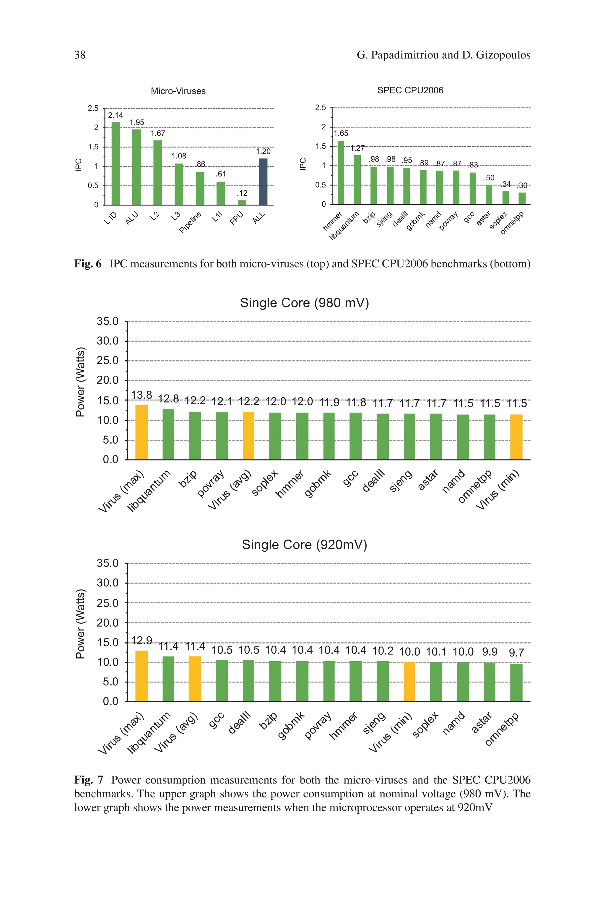
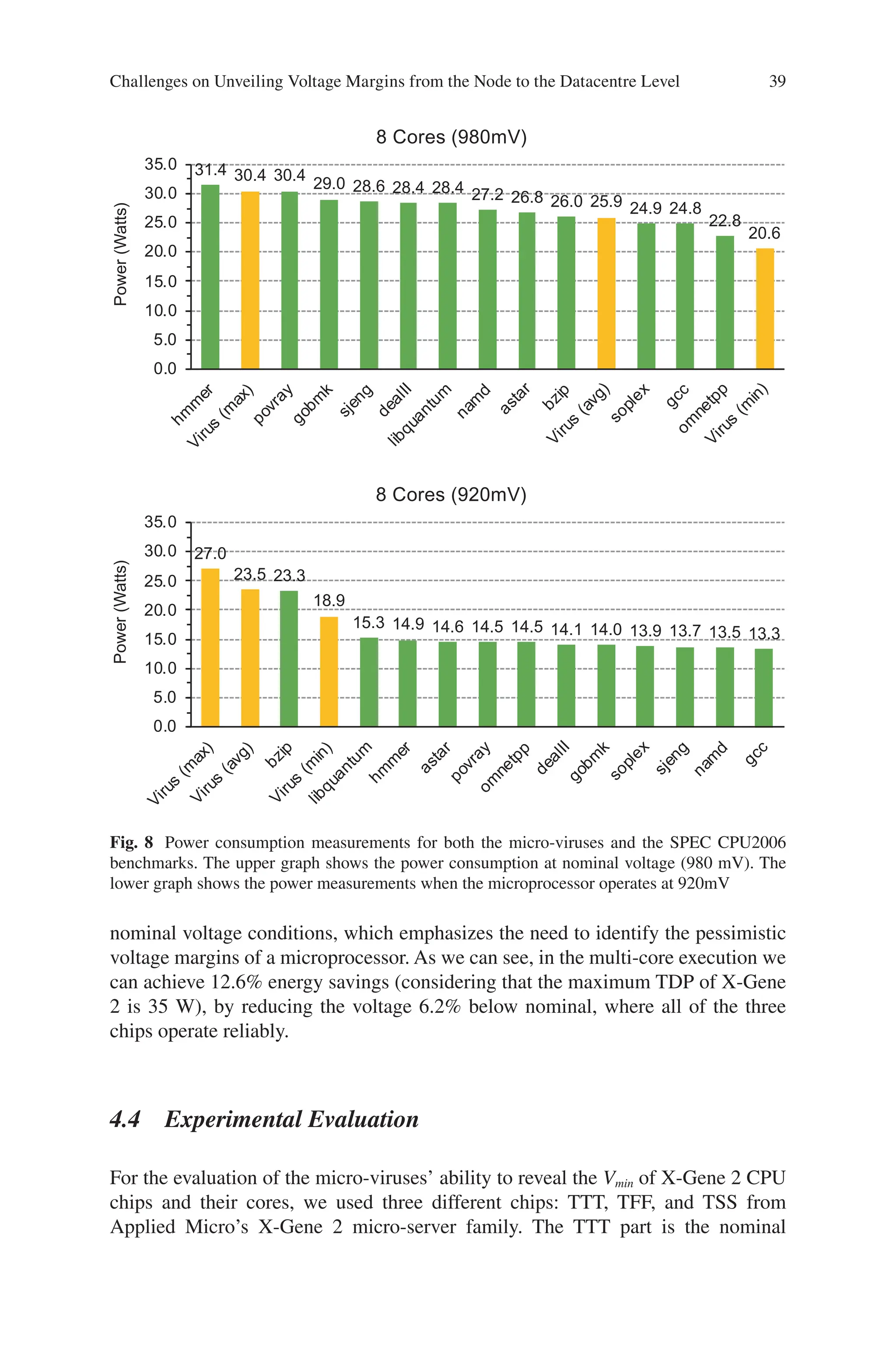
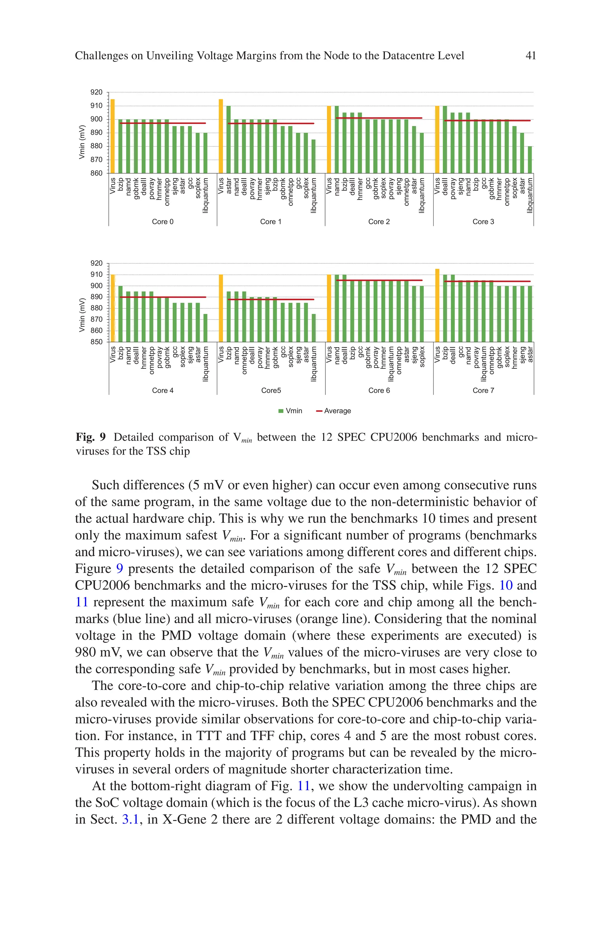
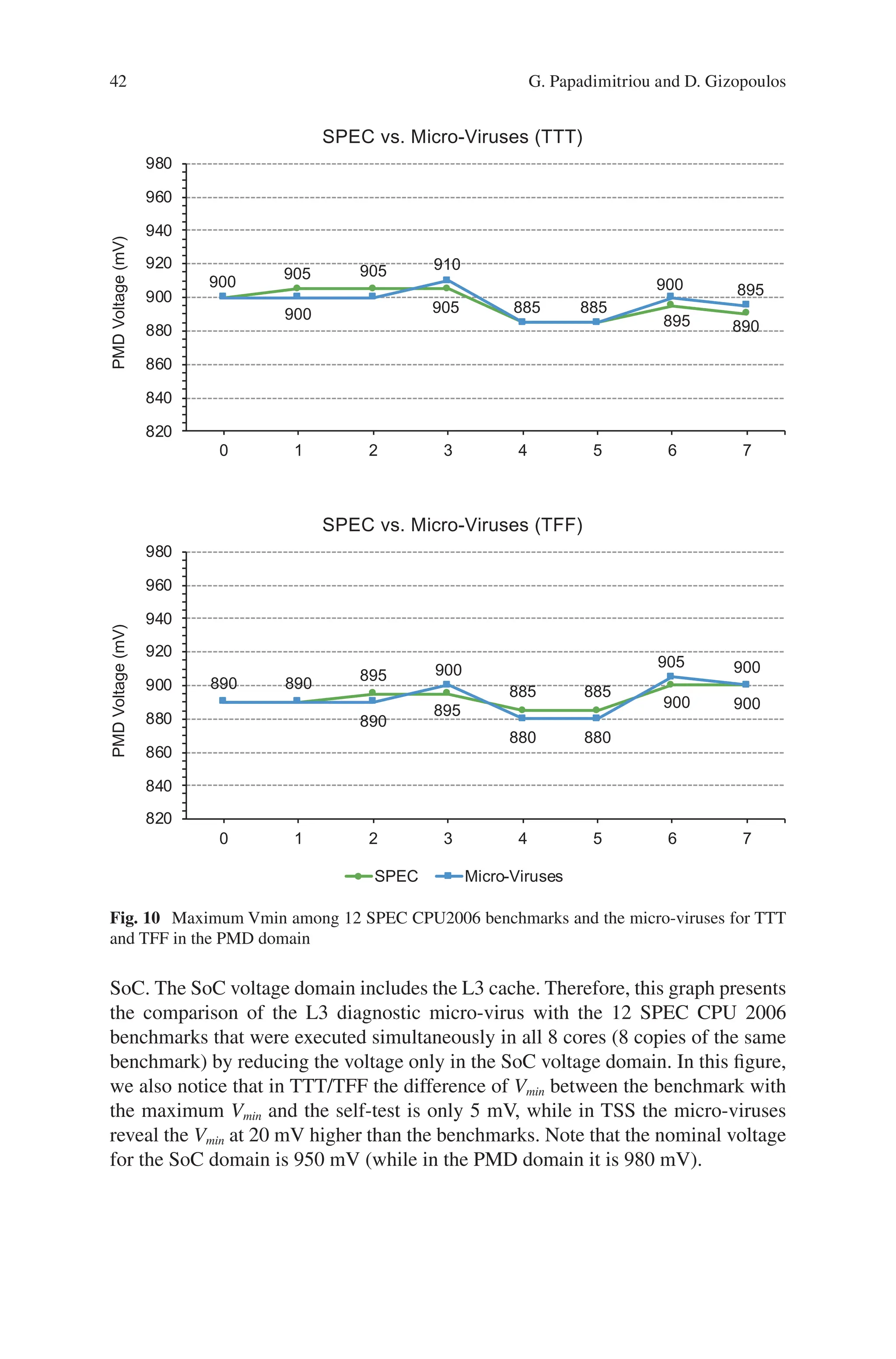
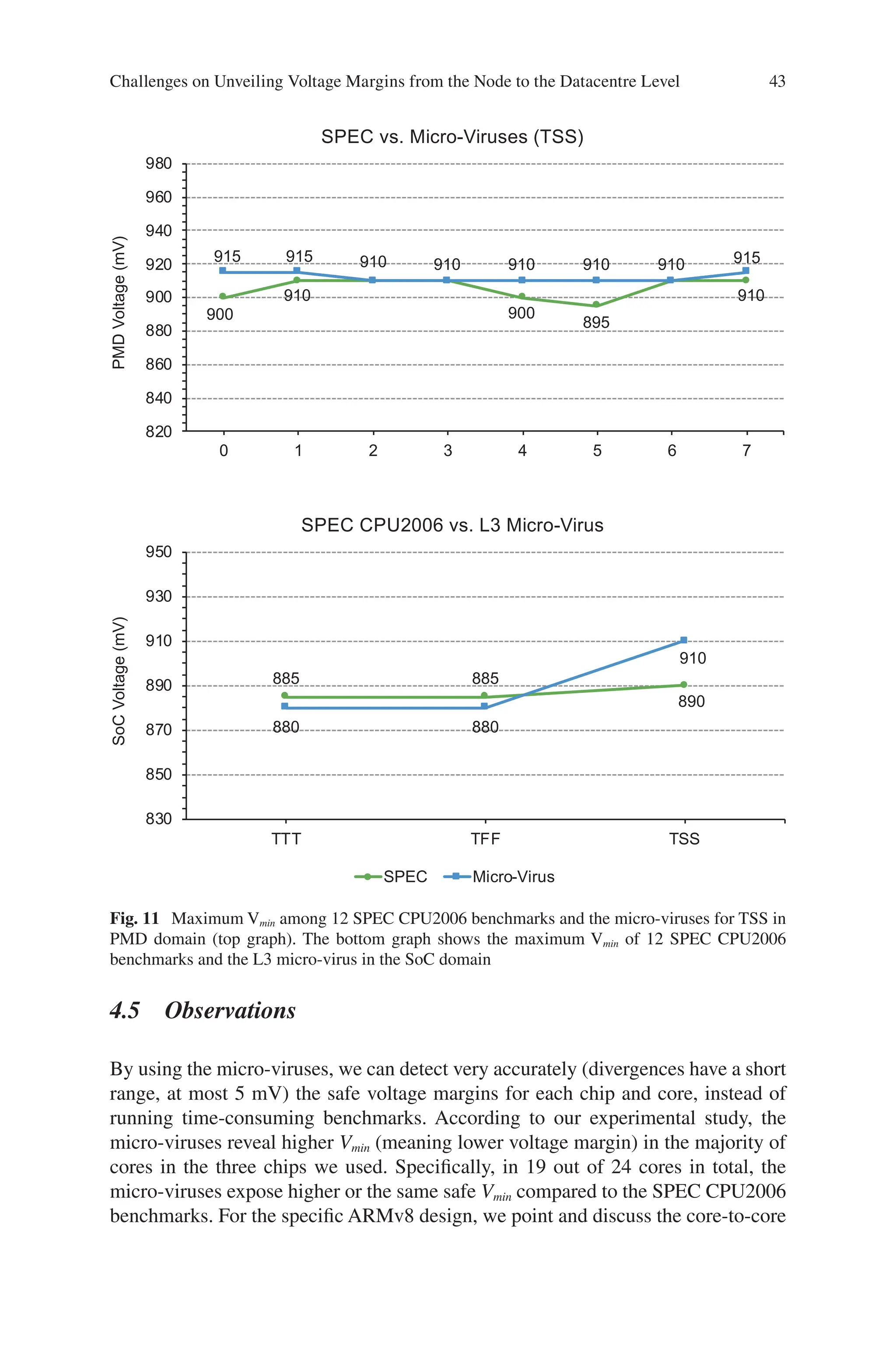
![44
and chip-to-chip variation, which are important to reduce the power consumption of
the microprocessor.
Core-to-Core Variation There are significant divergences among the cores due to
process variation. Process variation can affect transistor dimensions (length, width,
oxide thickness, etc.) which have a direct impact on the threshold voltage of a MOS
device, and thus, on the guardband of each core. We demonstrate that although
micro-viruses can reveal similar divergences as the benchmarks among the different
cores and chips, however, in most of the cases, micro-viruses expose lower diver-
gences among cores in contrast to time-consuming SPEC CPU2006 benchmarks.
As shown in Figs. 10 and 11, the micro-viruses reveal higher safe Vmin for all the
cores than the benchmarks, and also, we notice that the workload-to-workload dif-
ferences are up to 30 mV. Therefore, due to the diversity of code execution of
benchmarks, it is difficult to choose one benchmark that provides the highest Vmin.
Different benchmarks provide significantly different Vmin at different cores in
different chips. Therefore, a large number of different benchmarks are required to
reach a safe result concerning the voltage margins variability identification. Using
our micro-viruses, which fully stress the fundamental units of the microprocessor,
the cores guardbands can be safely determined (regarding the safe Vmin) at a very
short time, and guide energy efficiency when running typical applications.
Chip-to-Chip Variation As Figs. 10 and 11 present for the TTT and TFF chips,
PMD 2 (cores 4 and 5) is the most robust PMD for all three chips (it can tolerate up
to 3.6% more undervolting compared to the most sensitive cores). We can notice
that (on average among all cores of the same chip) the TFF chip has lower Vmin
points than the TTT chip, in contrast to the TSS chip, which has higher Vmin points
than the other two chips, and thus, can deliver smaller power savings.
Diagnosis By using the diagnostic micro-viruses we can also determine if and
where an error or a silent data corruption (SDC) occurred. Through this component-
focused stress process we have observed the following:
(a) SDCs occur when the pipeline gets stressed (ALU, FPU, and Pipeline tests).
(b) The cache bit-cells operate safely at higher voltages (the caches tests crash
lower than the ALU and FPU tests).
Both observations show that the X-Gene 2 is more susceptible to timing-path
failures than to SRAM array failures. A major finding of our analysis using the
micro-viruses for ARMv8-compliant multicore CPUs is that SDCs (derived from
pipeline stressing using theALU, FPU, and Pipeline micro-viruses) appear at higher
voltage levels than corrected errors when cache arrays get stressed by cache-related
micro-viruses. We believe that the reason is that unlike other server-based CPUs
(like Itanium), X-Gene 2 does not deploy circuit-level techniques (Itanium performs
continuous clock-path de-skewing during dynamic operation) [64], and thereby,
when the pipeline gets stressed, X-Gene 2 produces SDCs due to timing-path
failures.
G. Papadimitriou and D. Gizopoulos](https://image.slidesharecdn.com/23098776-250511125104-f114a86f/75/Computing-At-The-Edge-New-Challenges-For-Service-Provision-Georgios-Karakonstantis-54-2048.jpg)