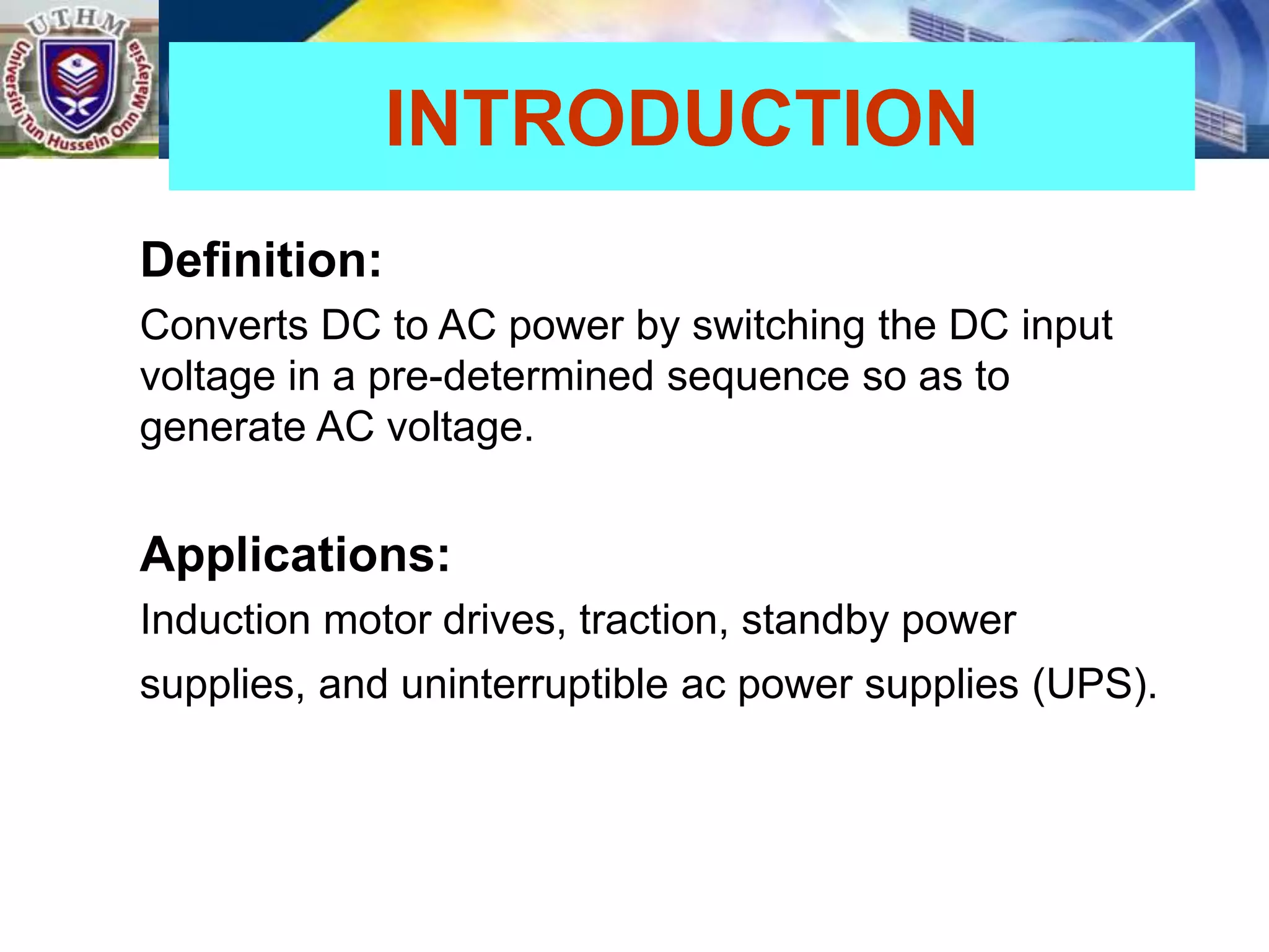
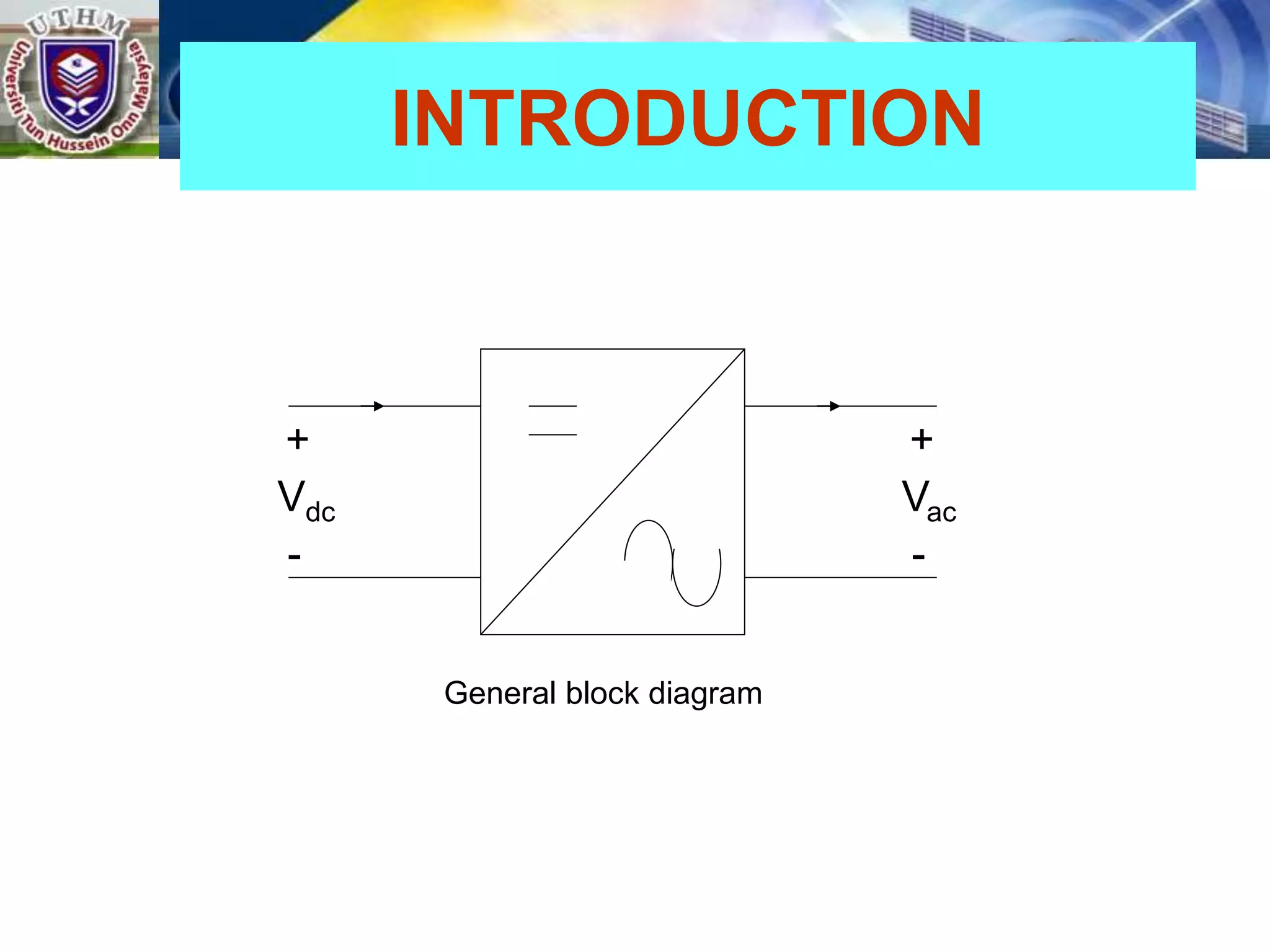
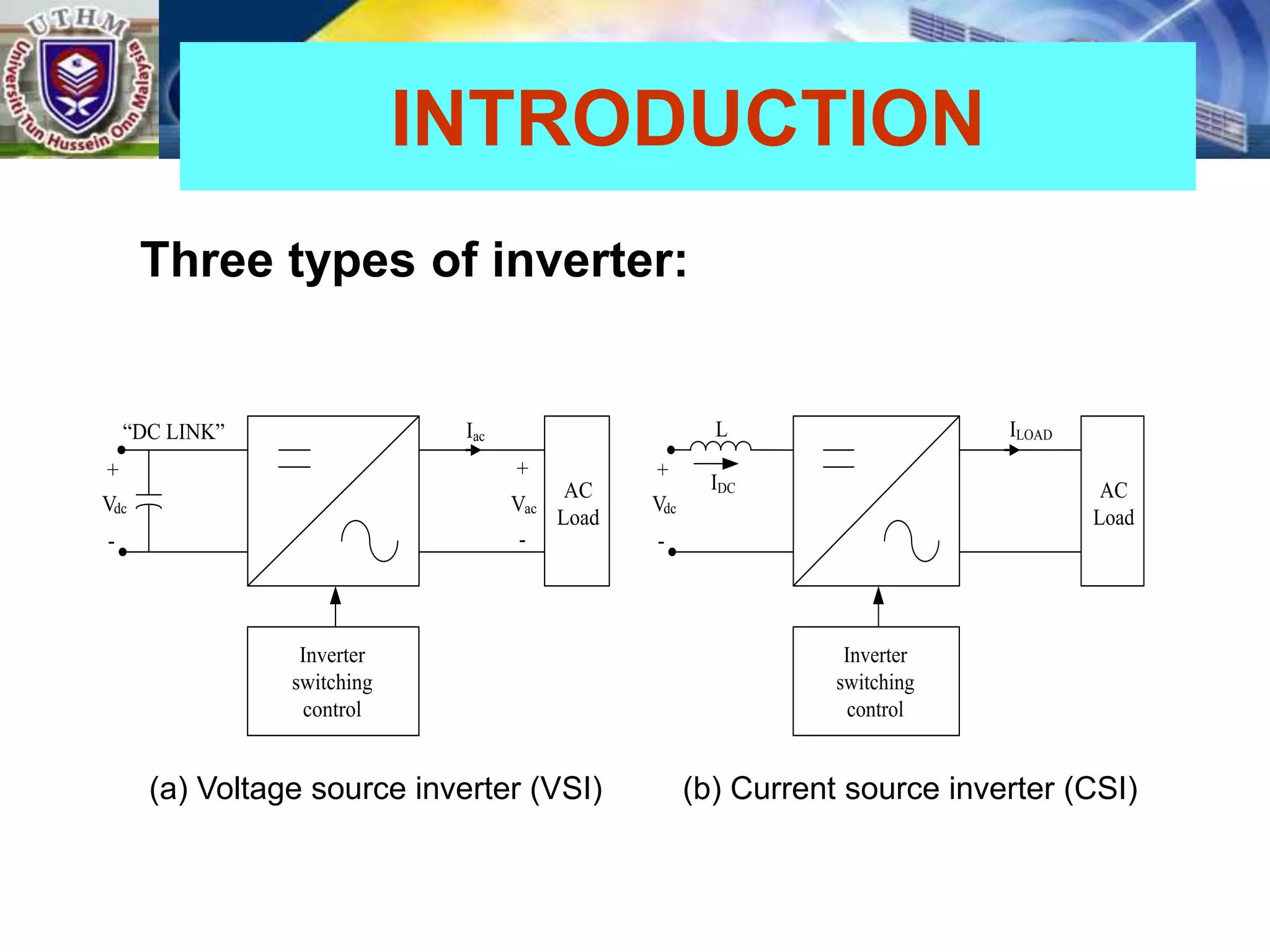
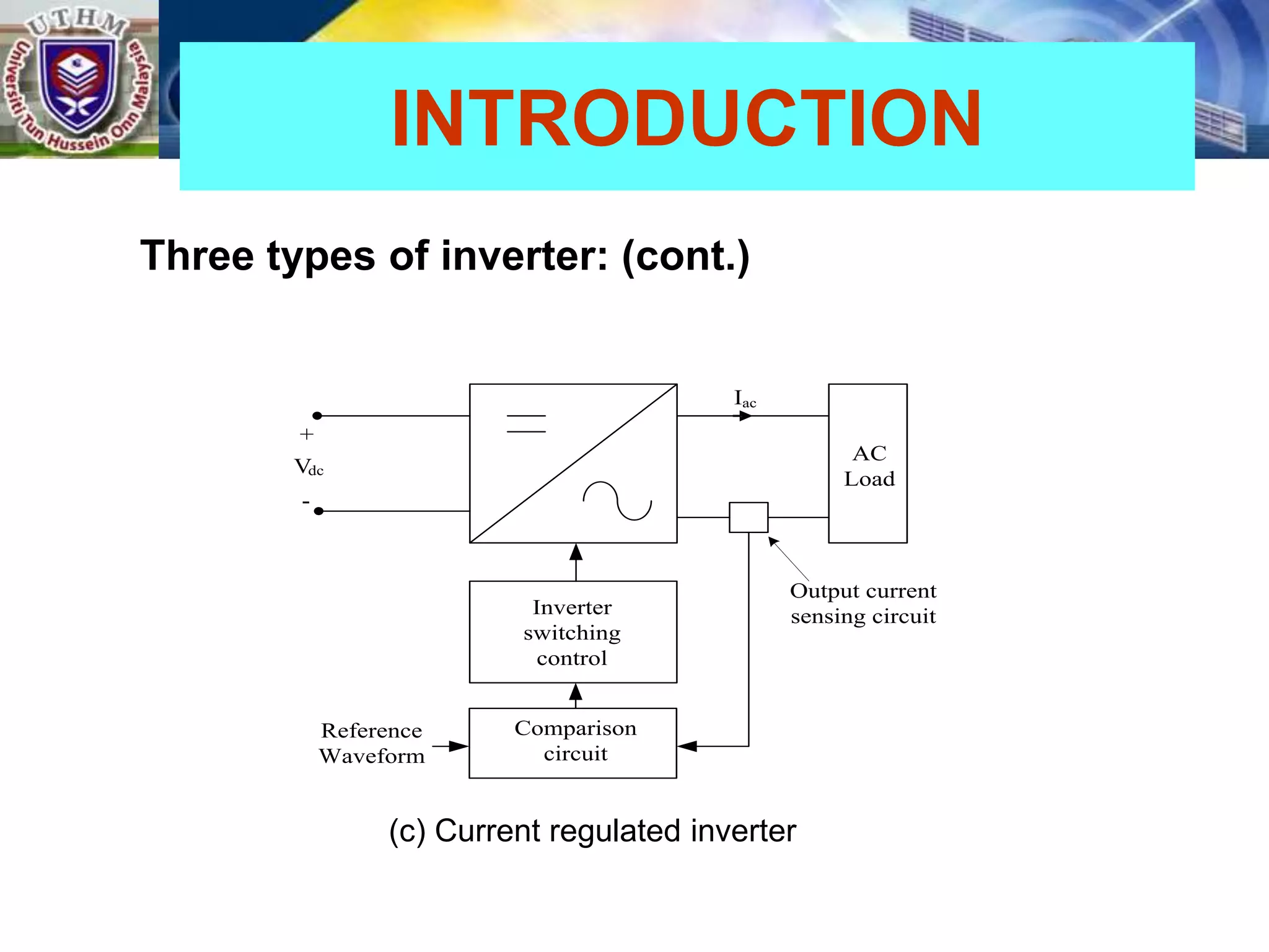
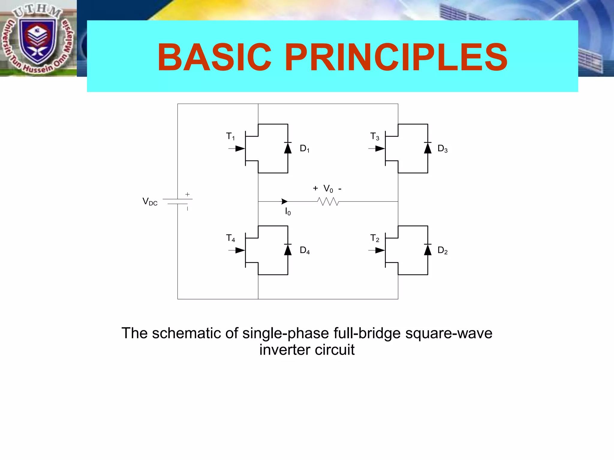
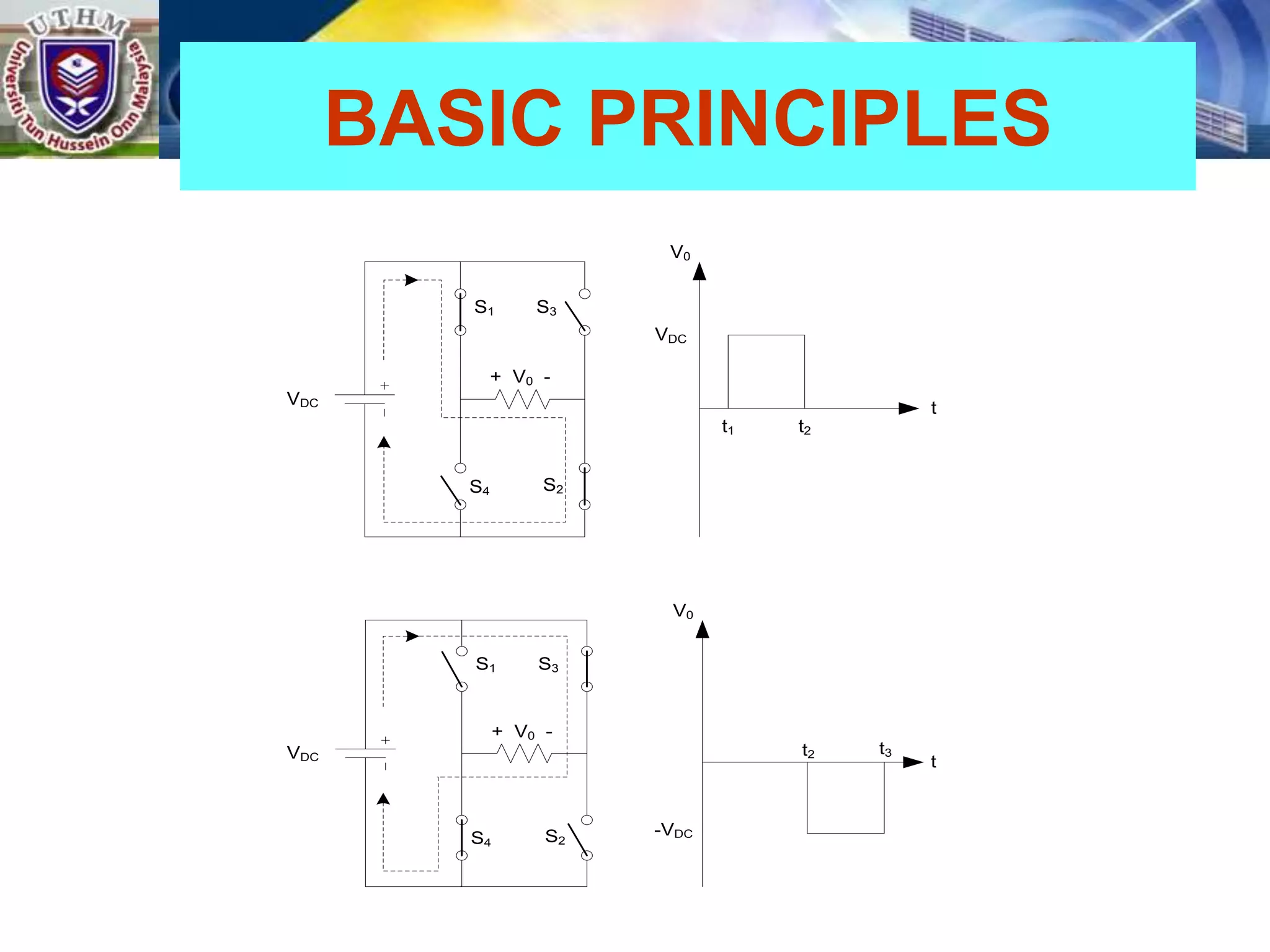
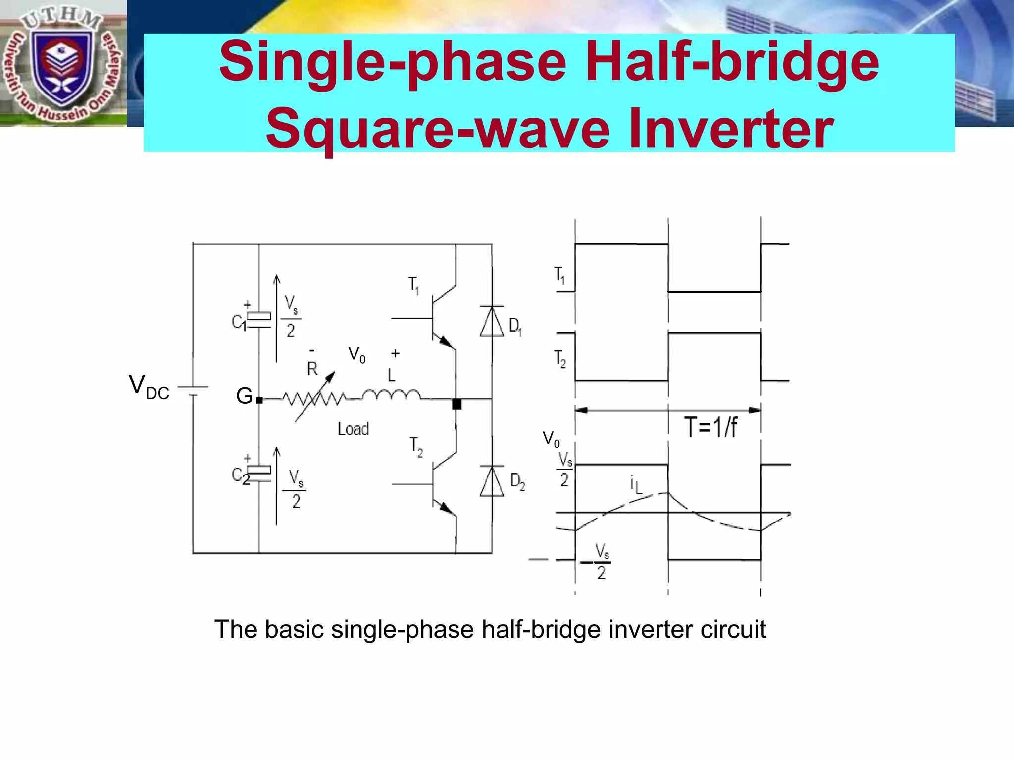
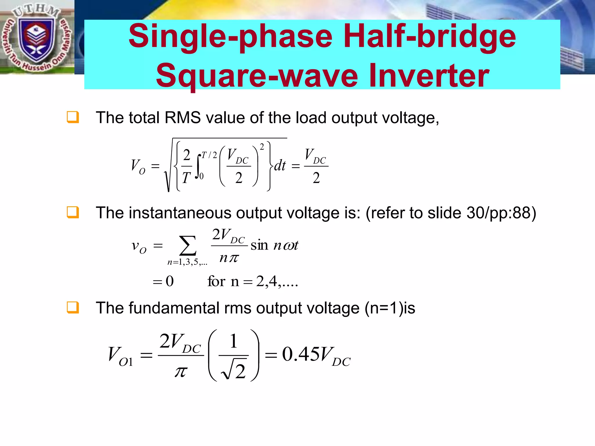
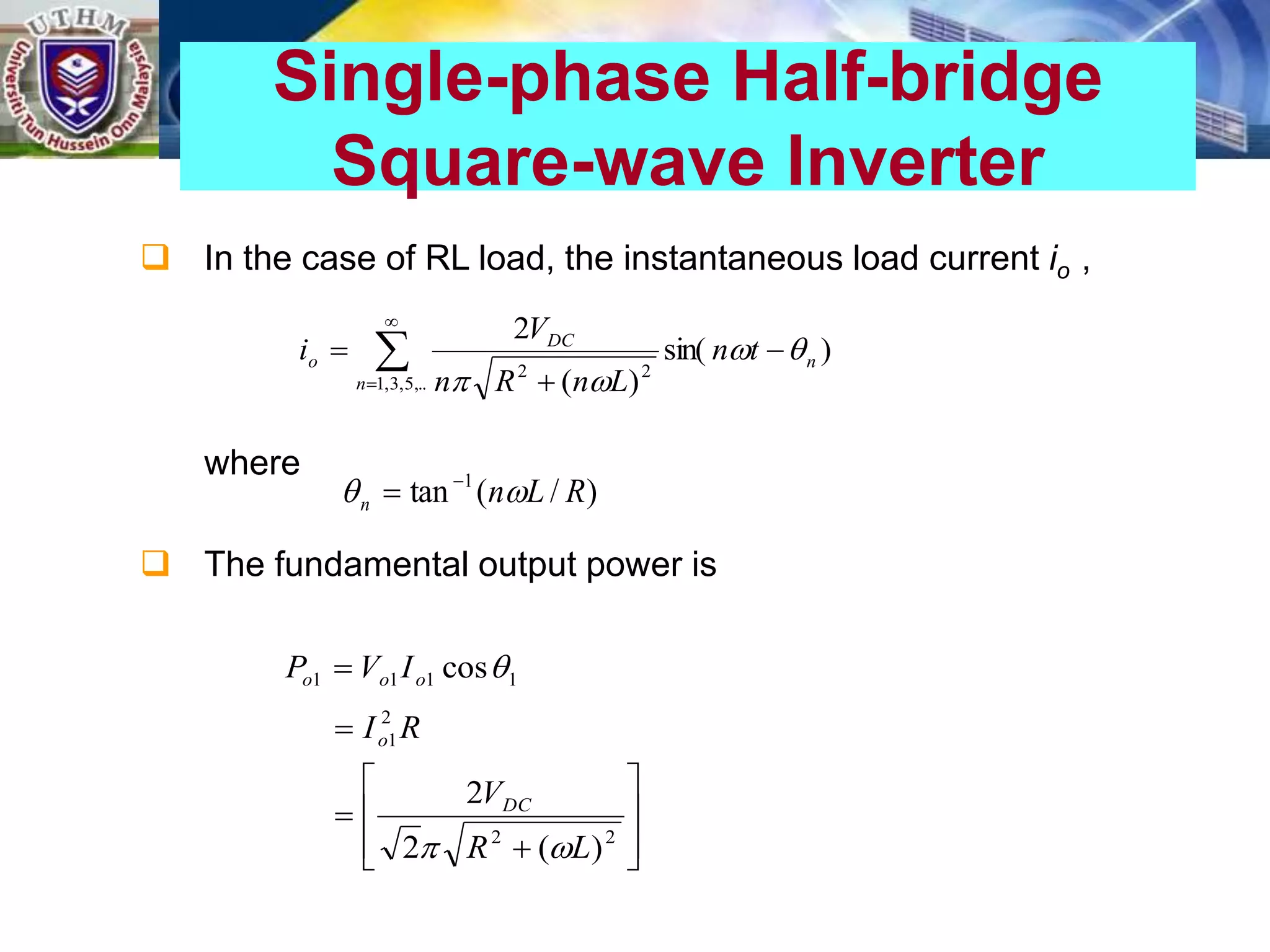
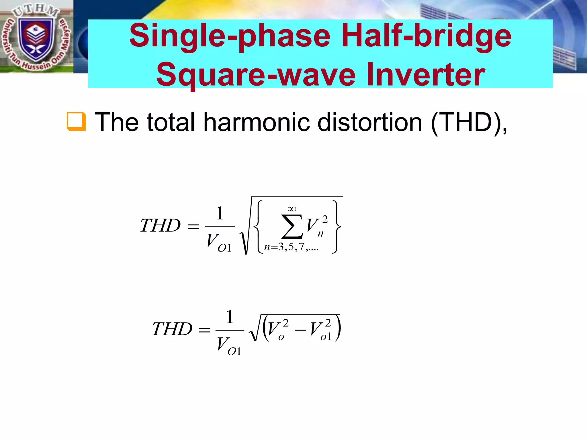
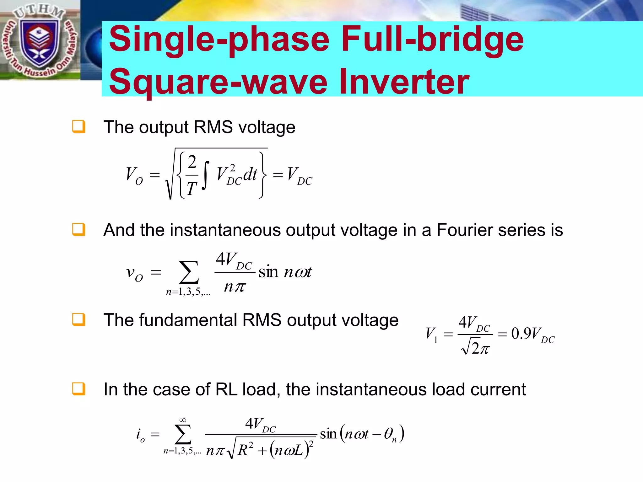
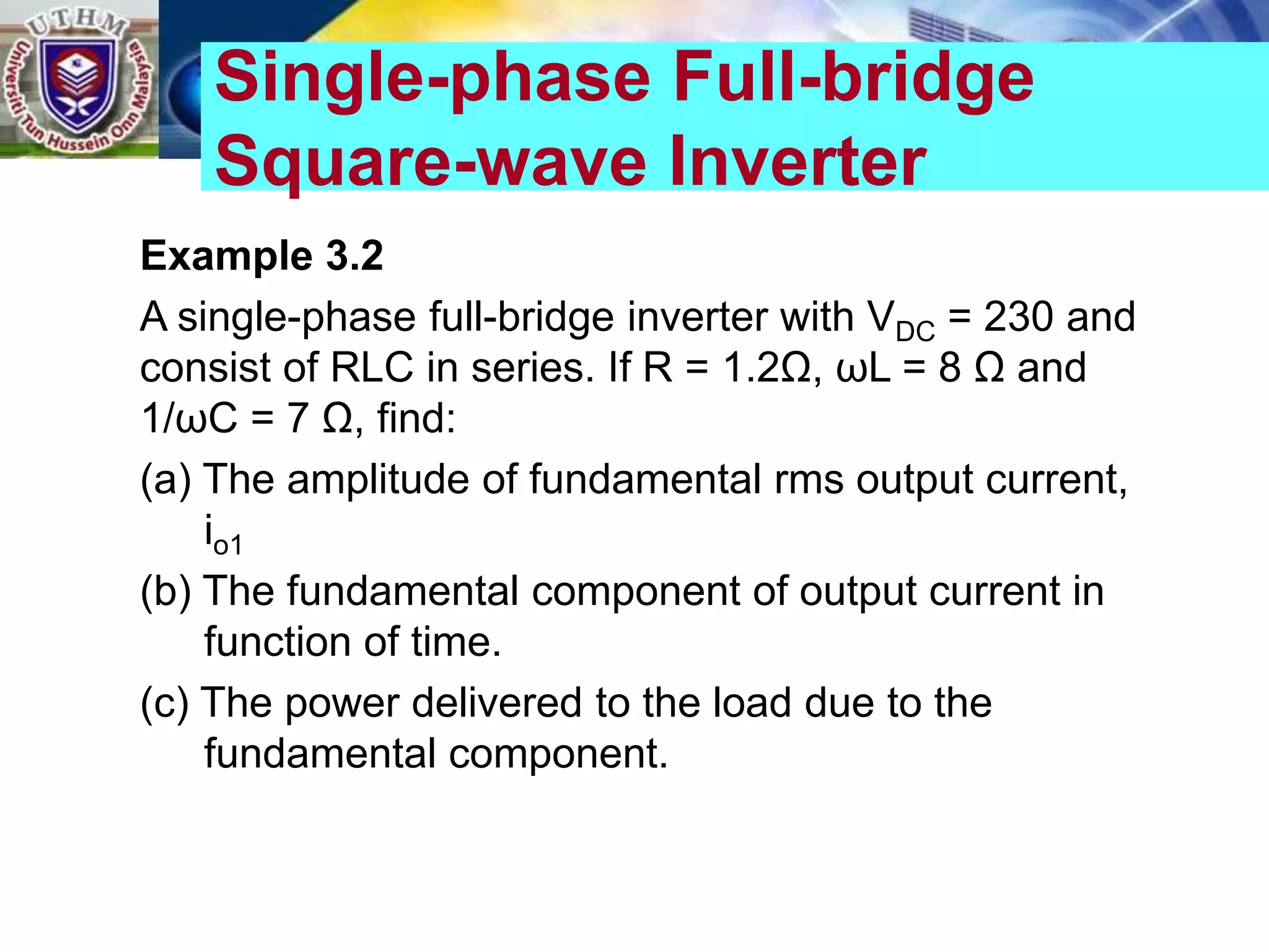
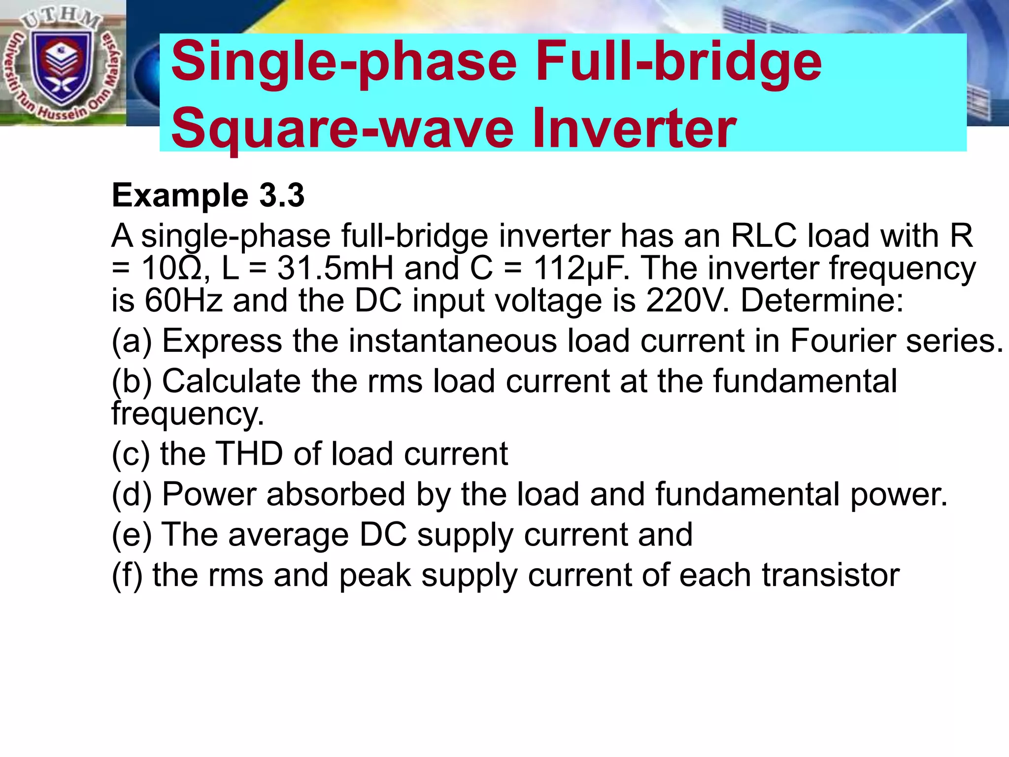
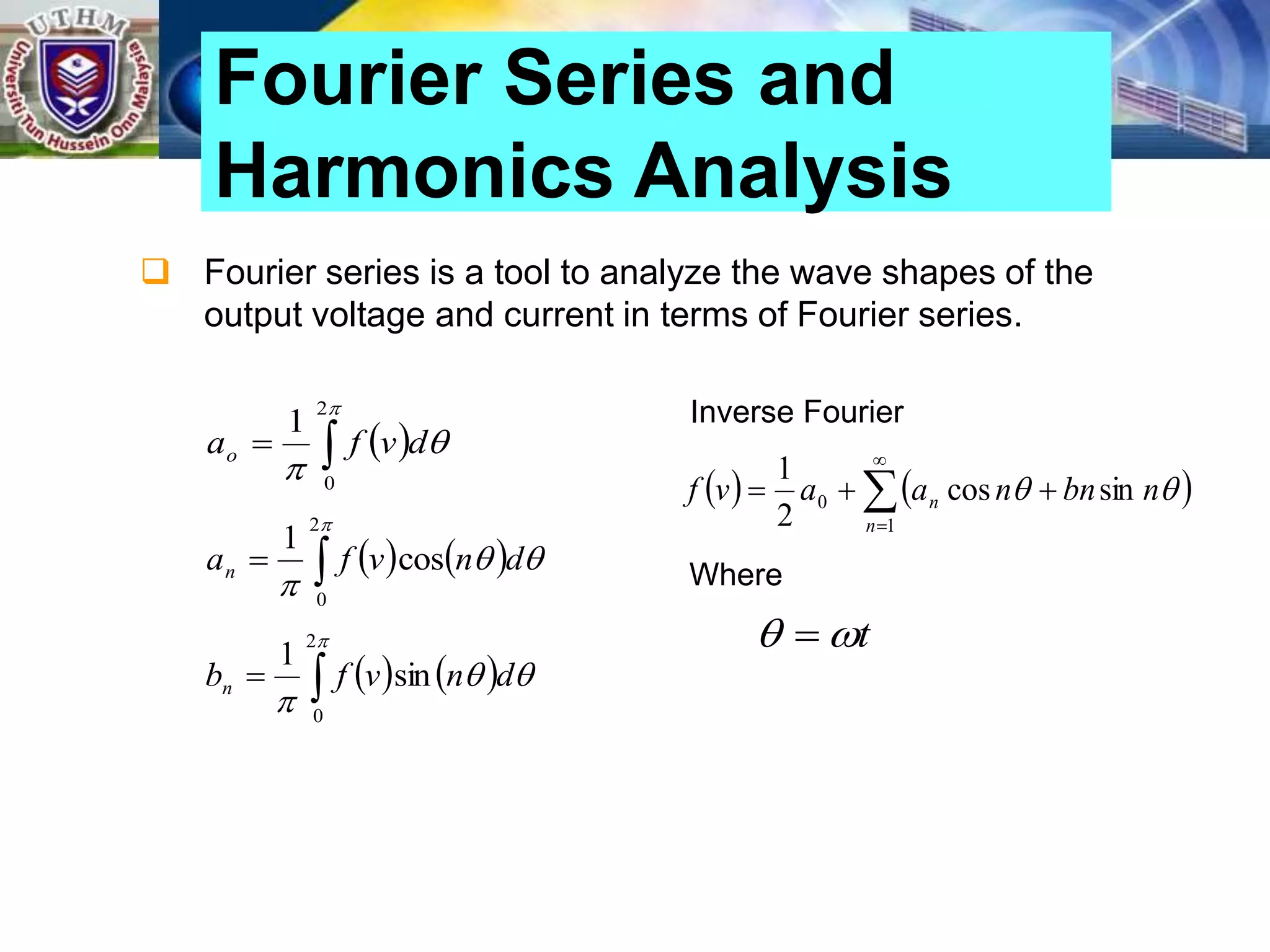
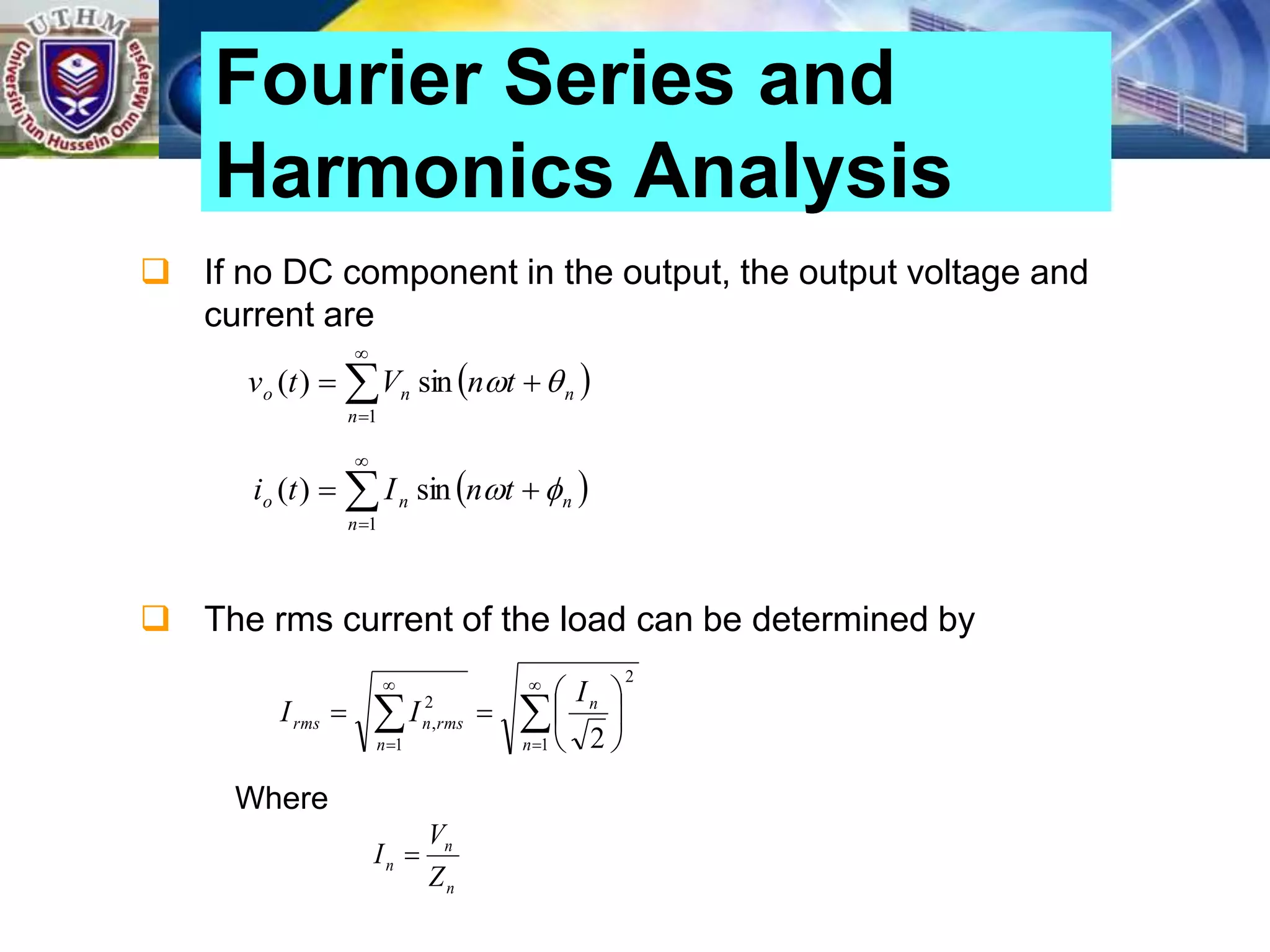
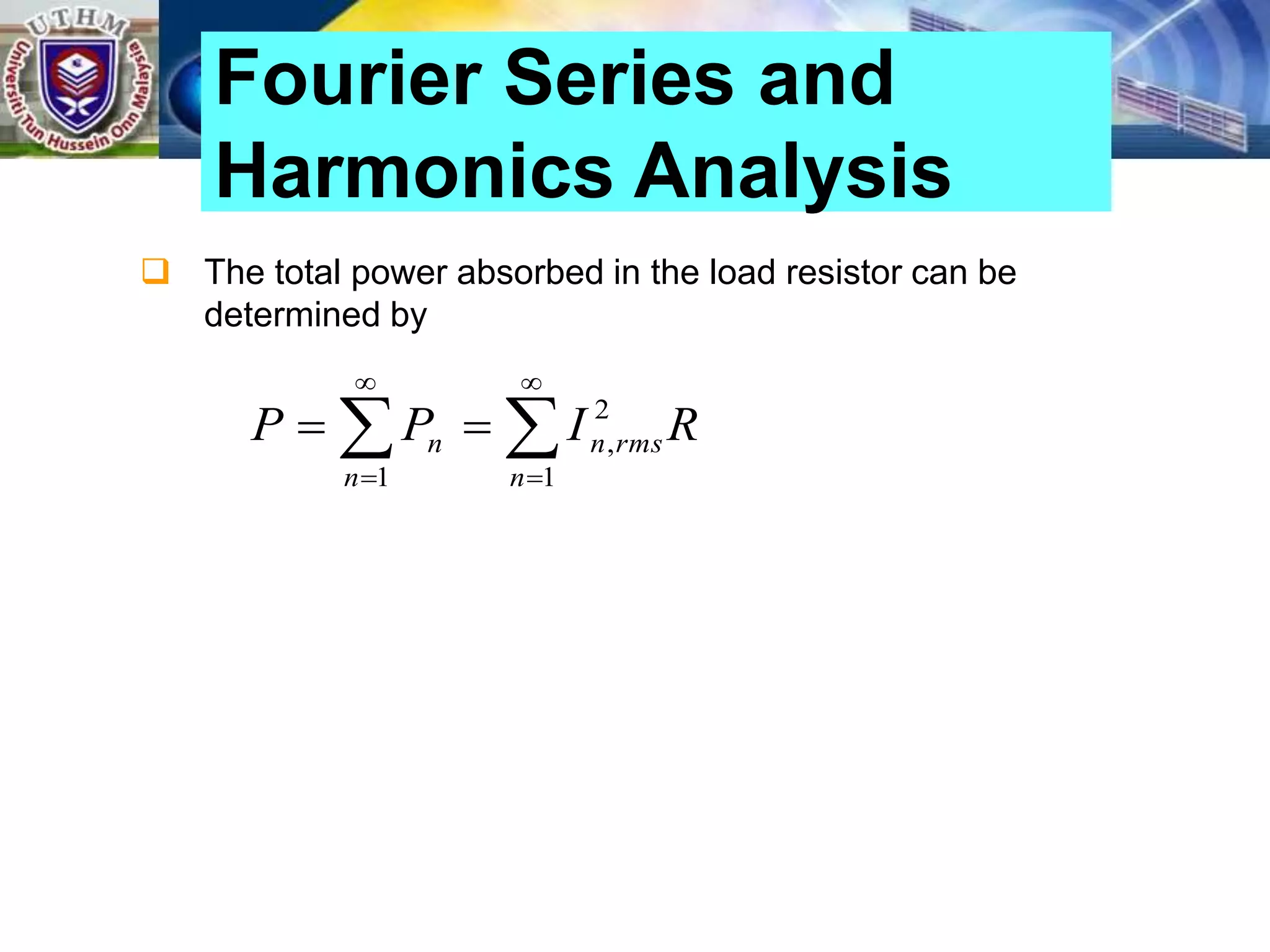
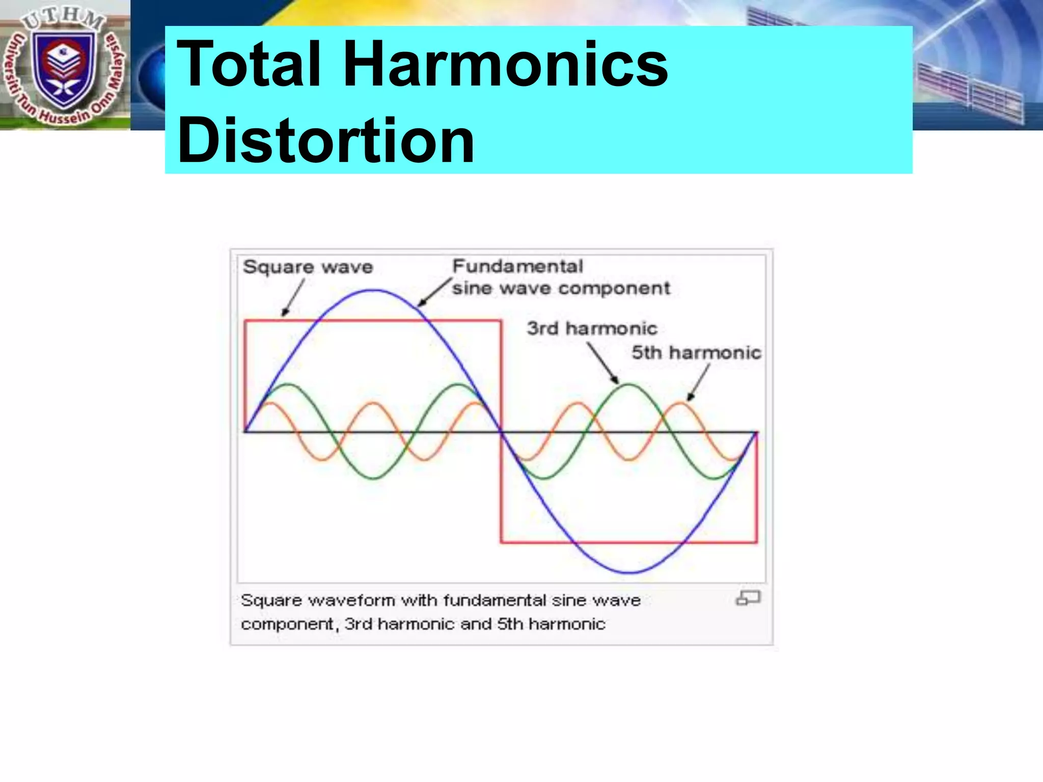
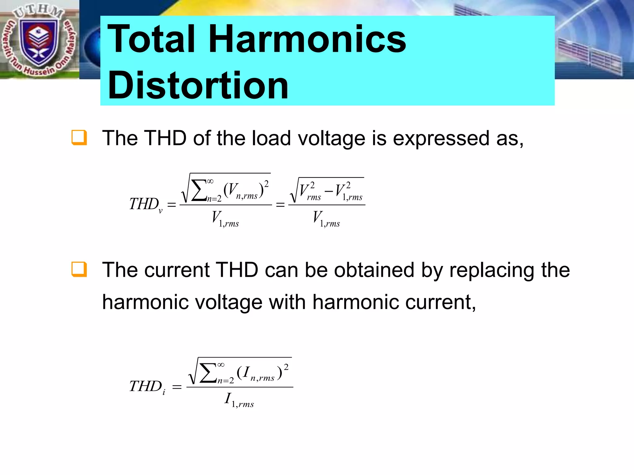
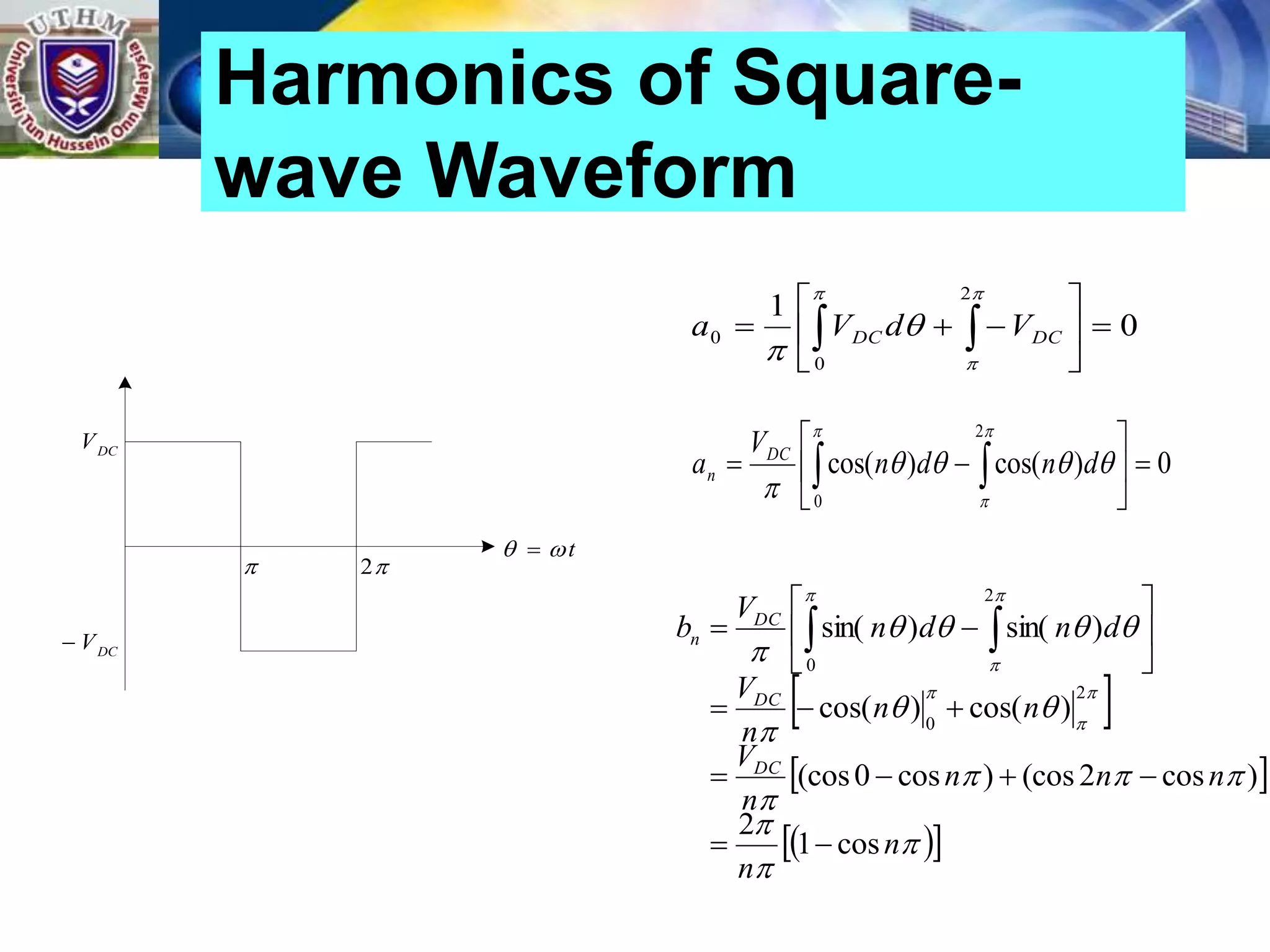
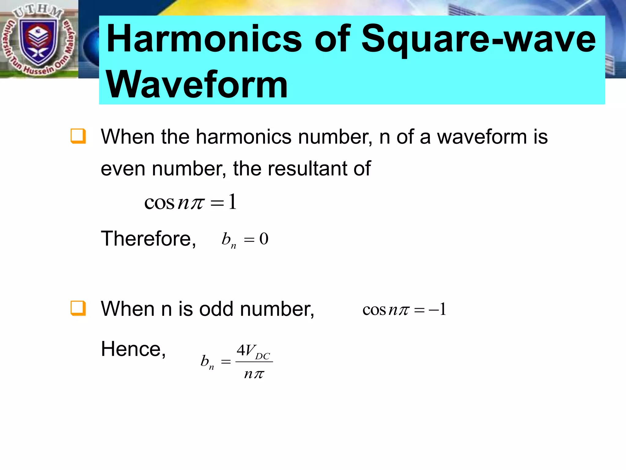
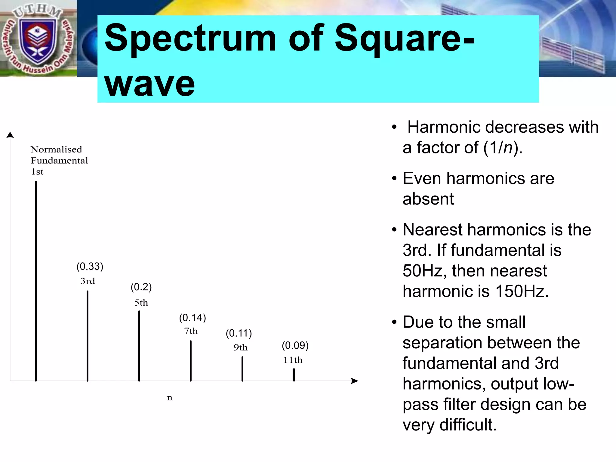
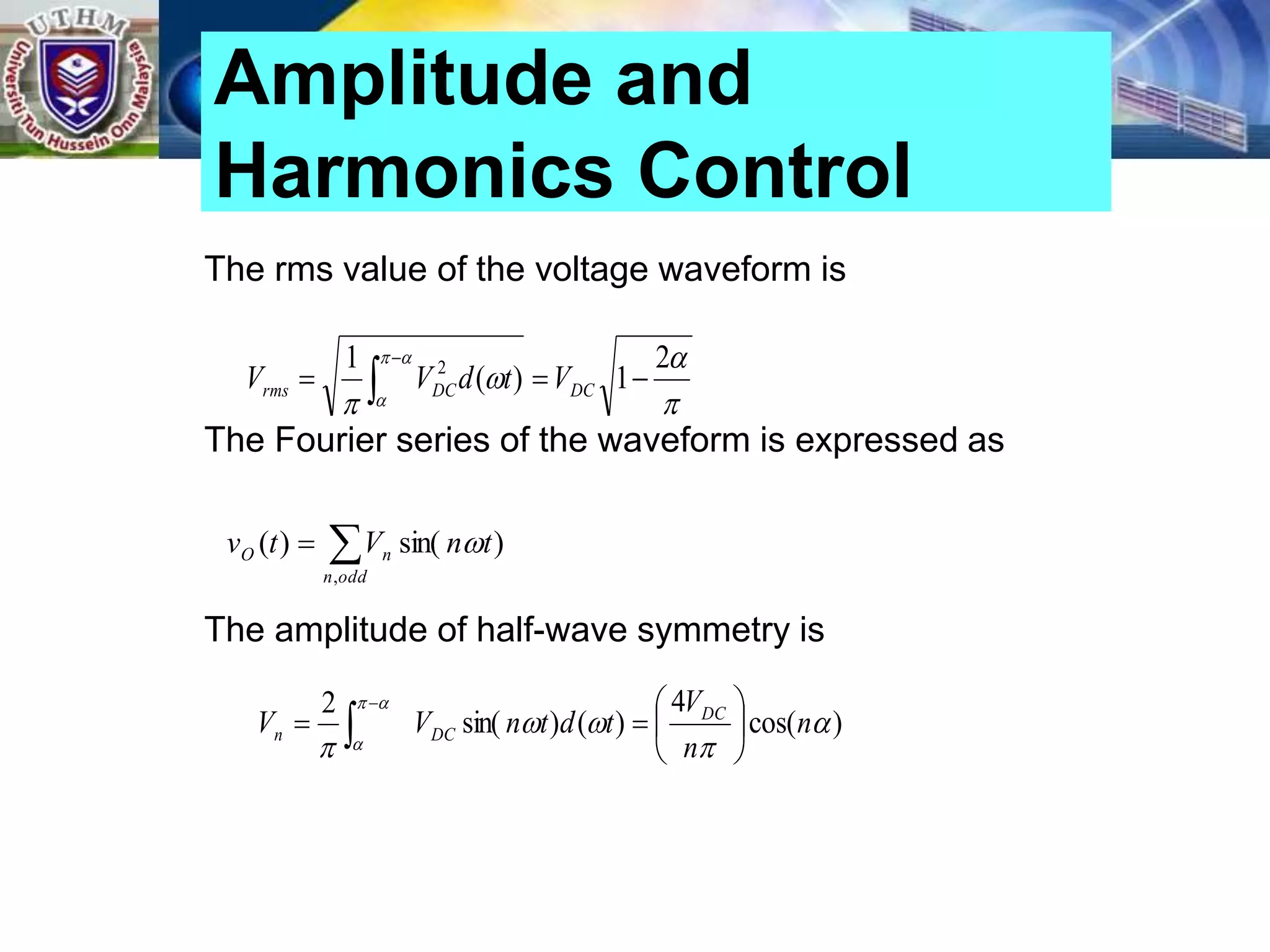
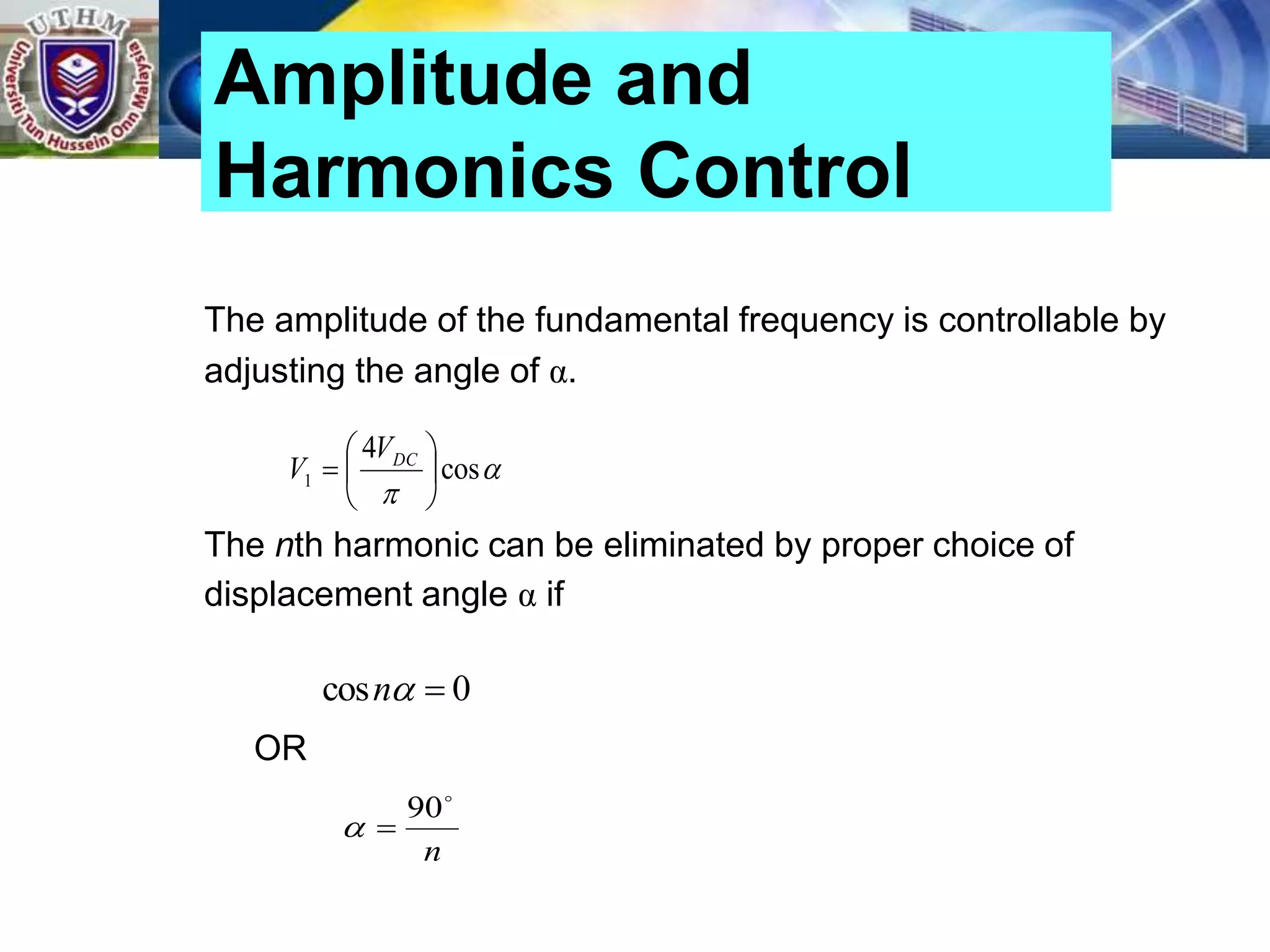
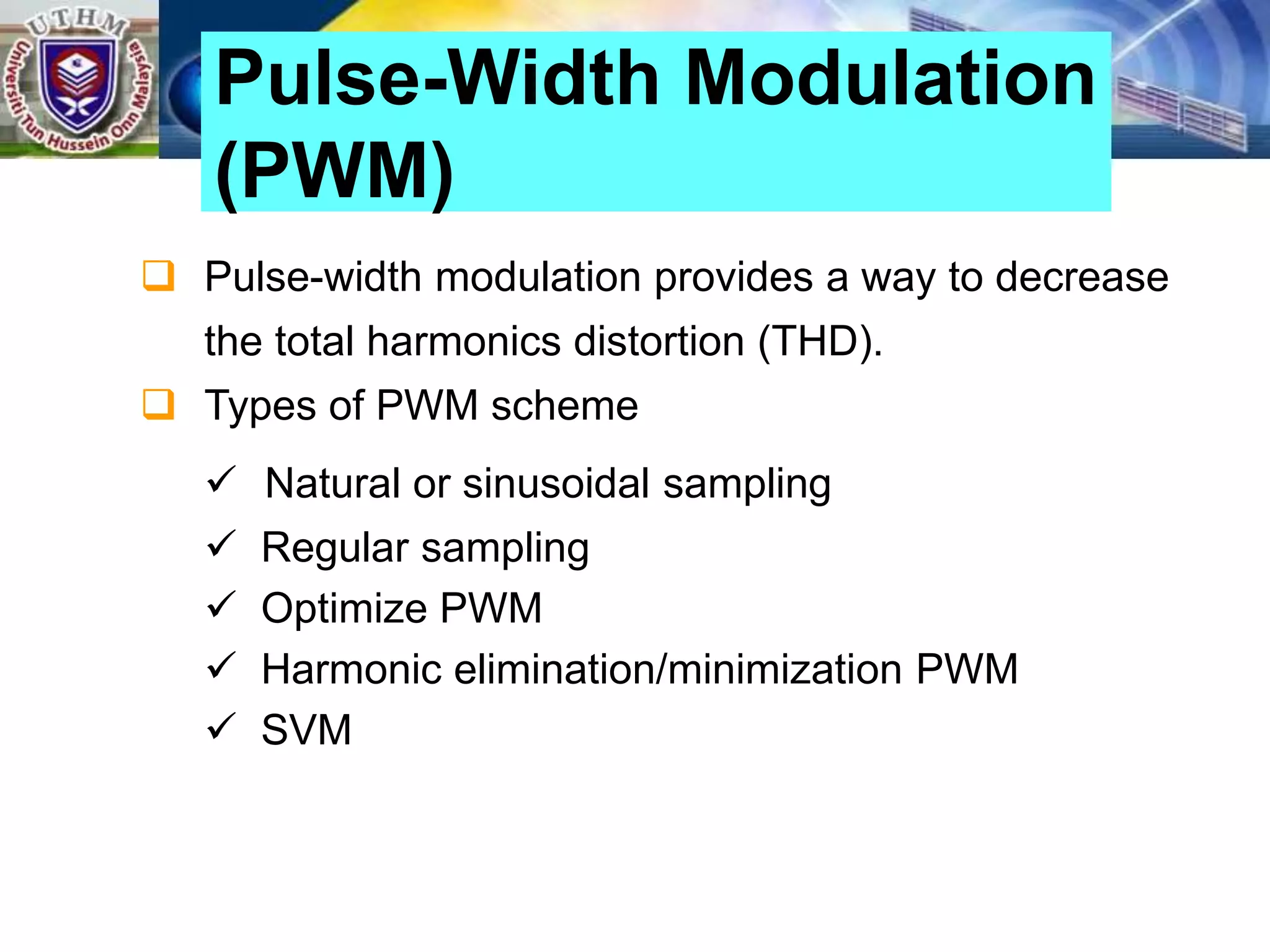
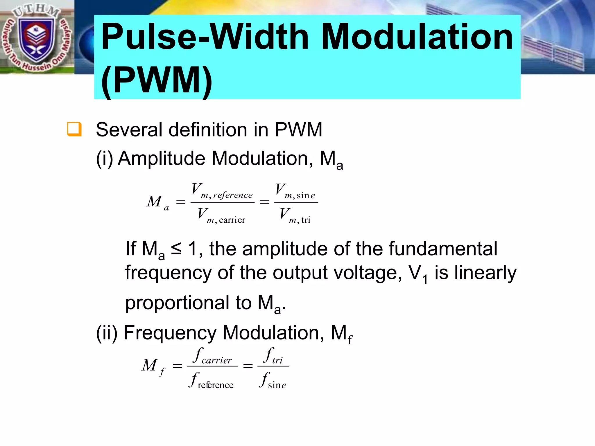
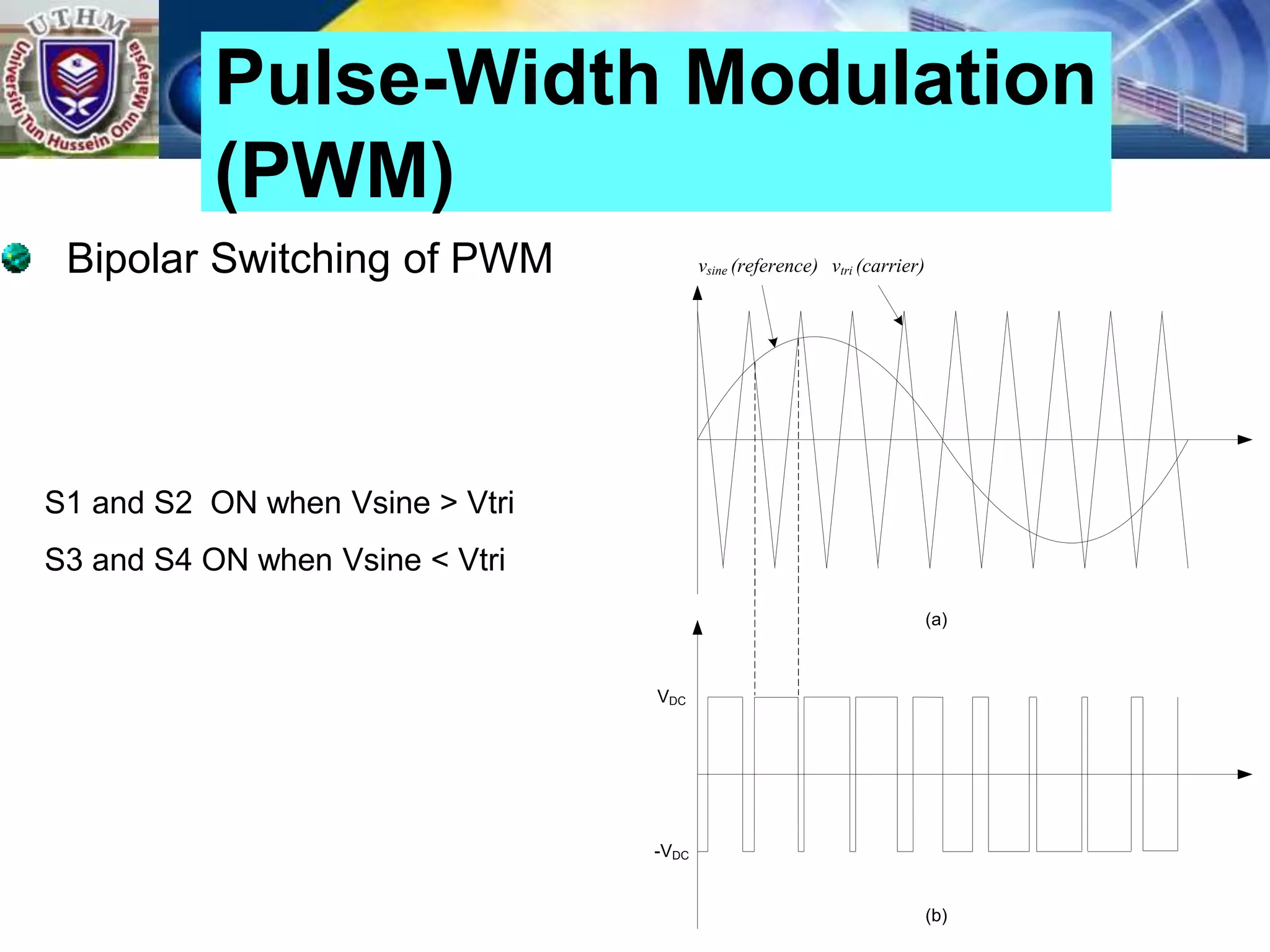
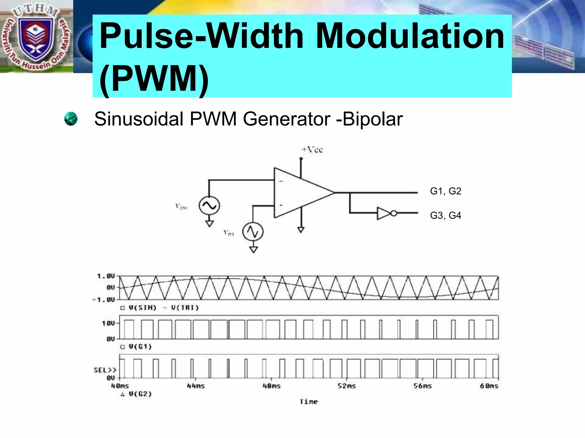
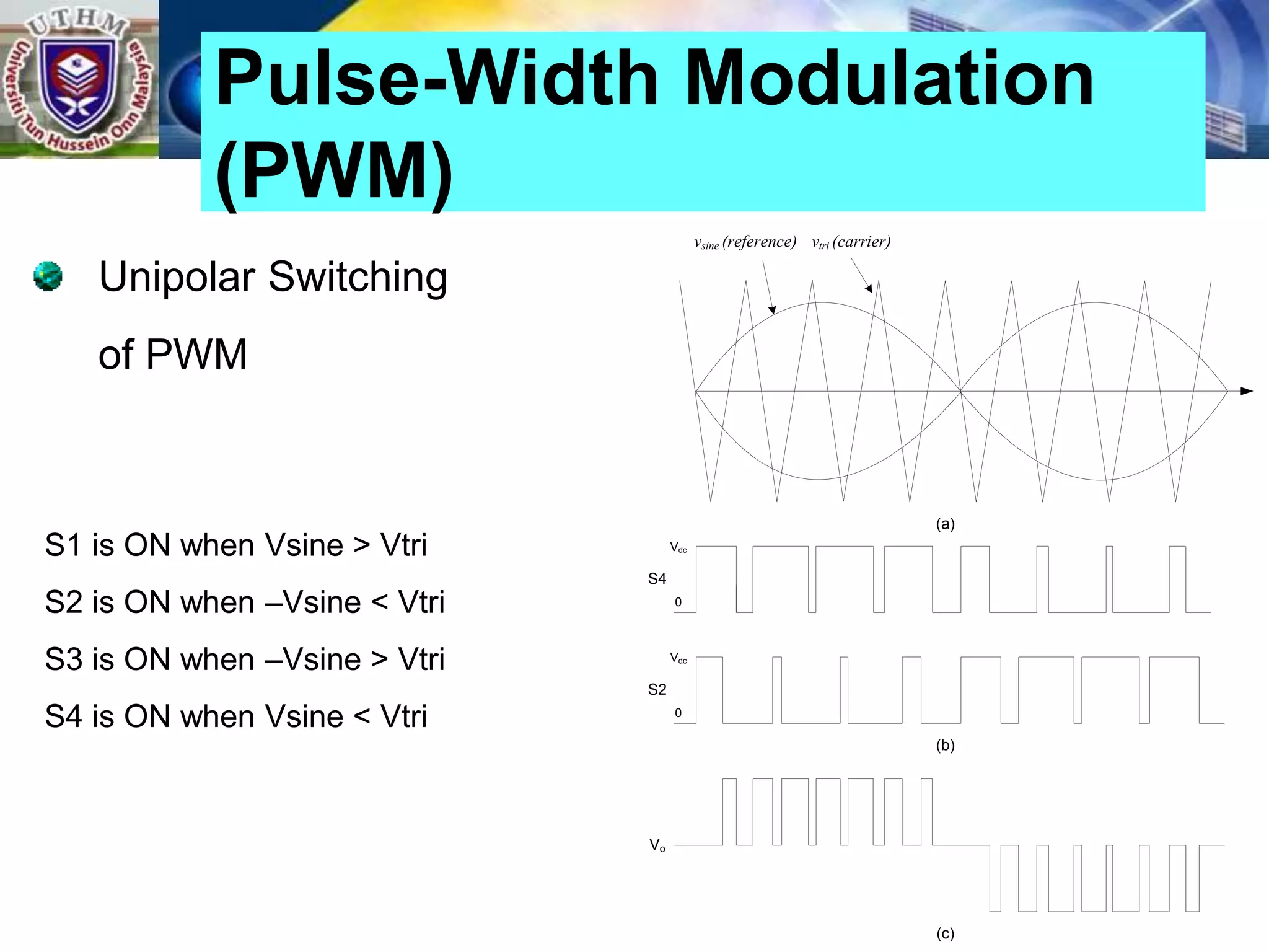
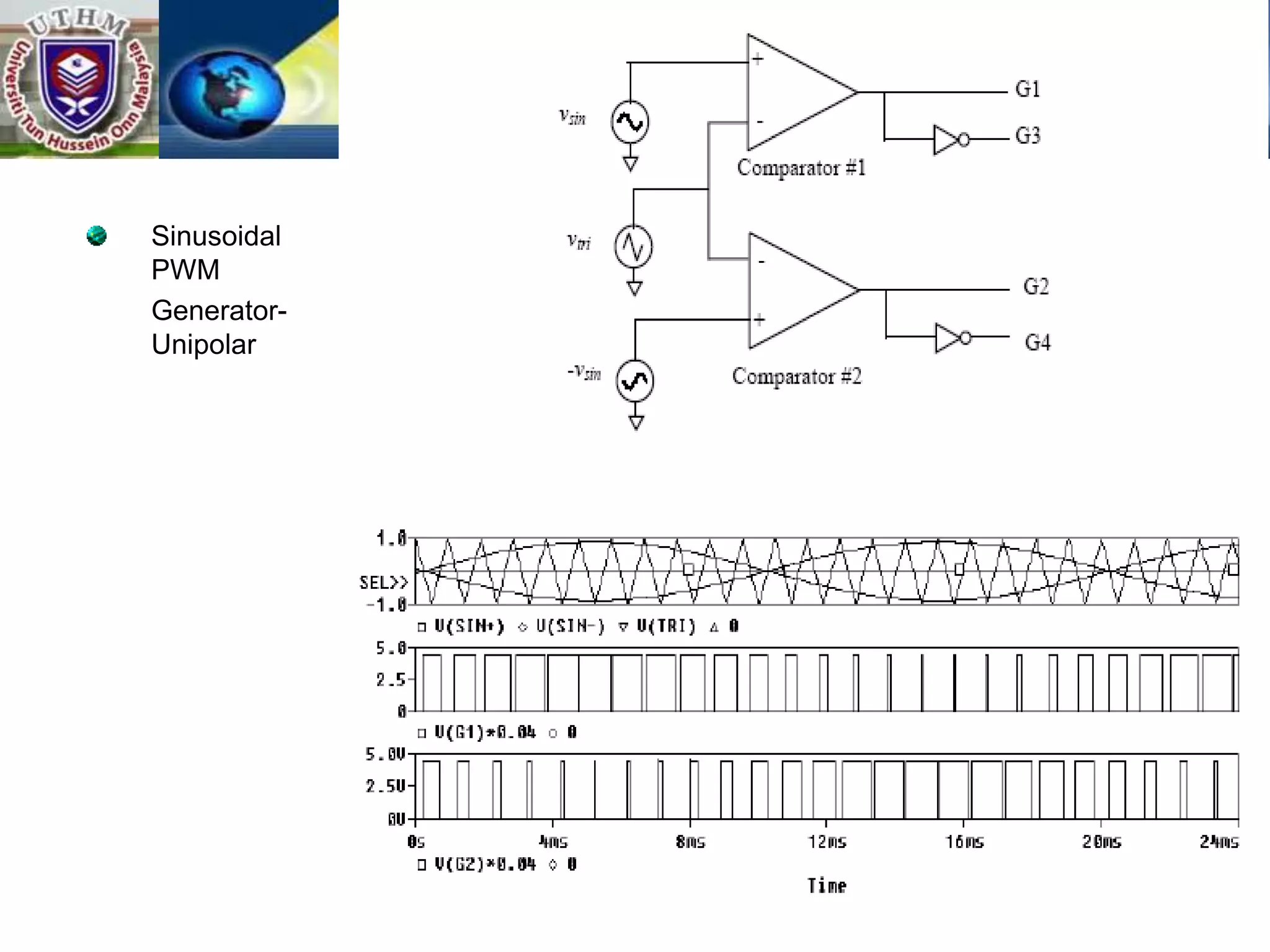
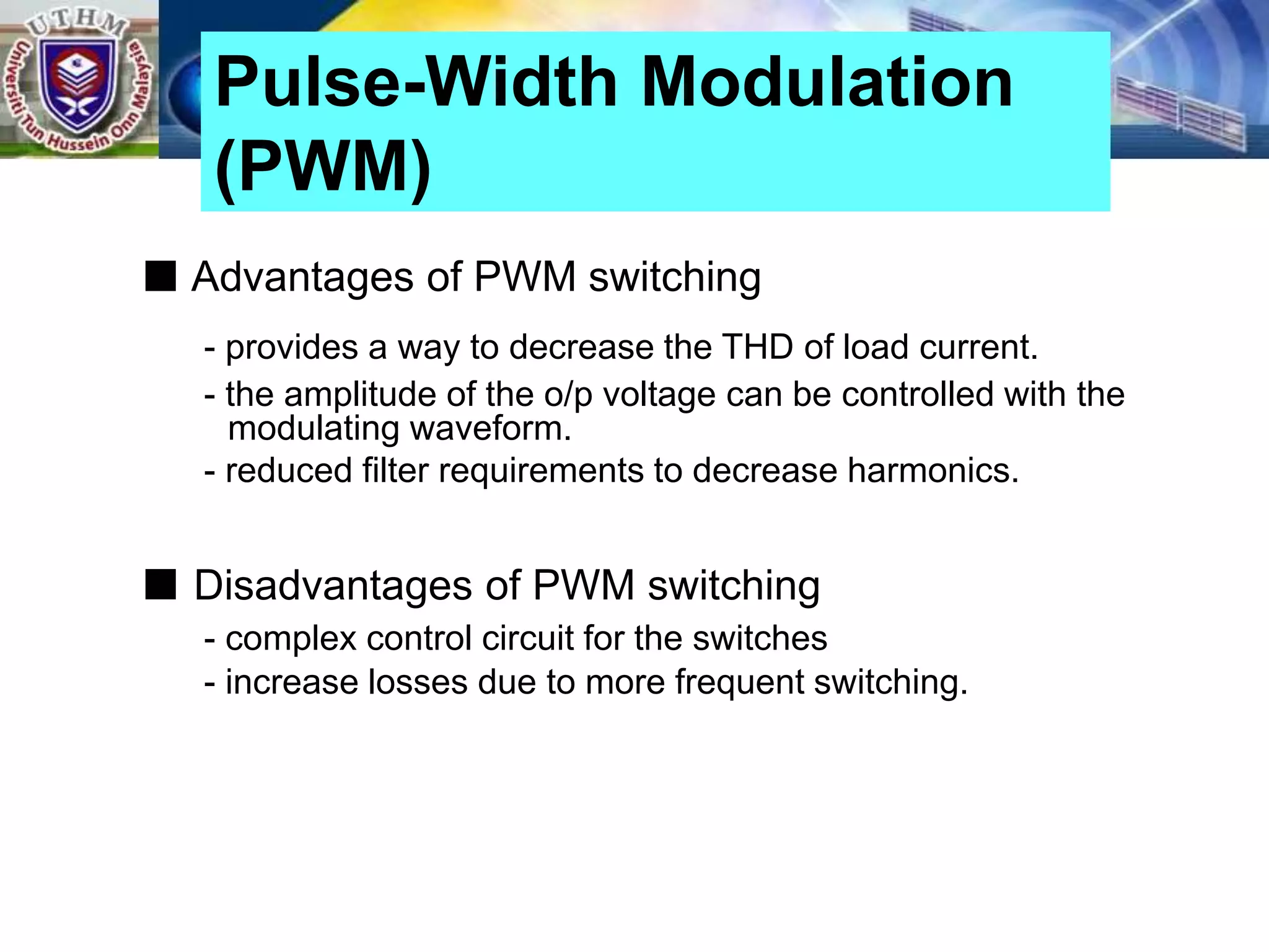
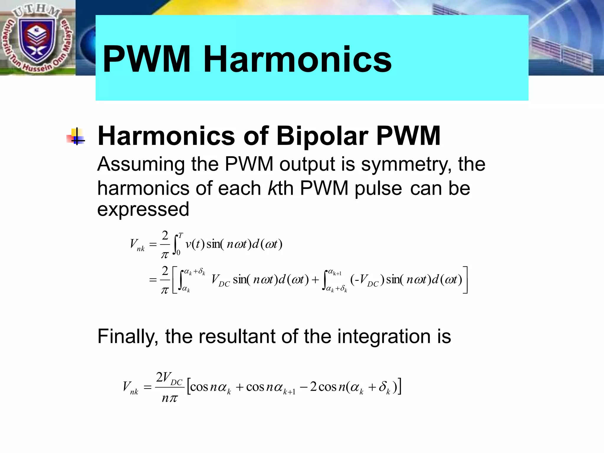
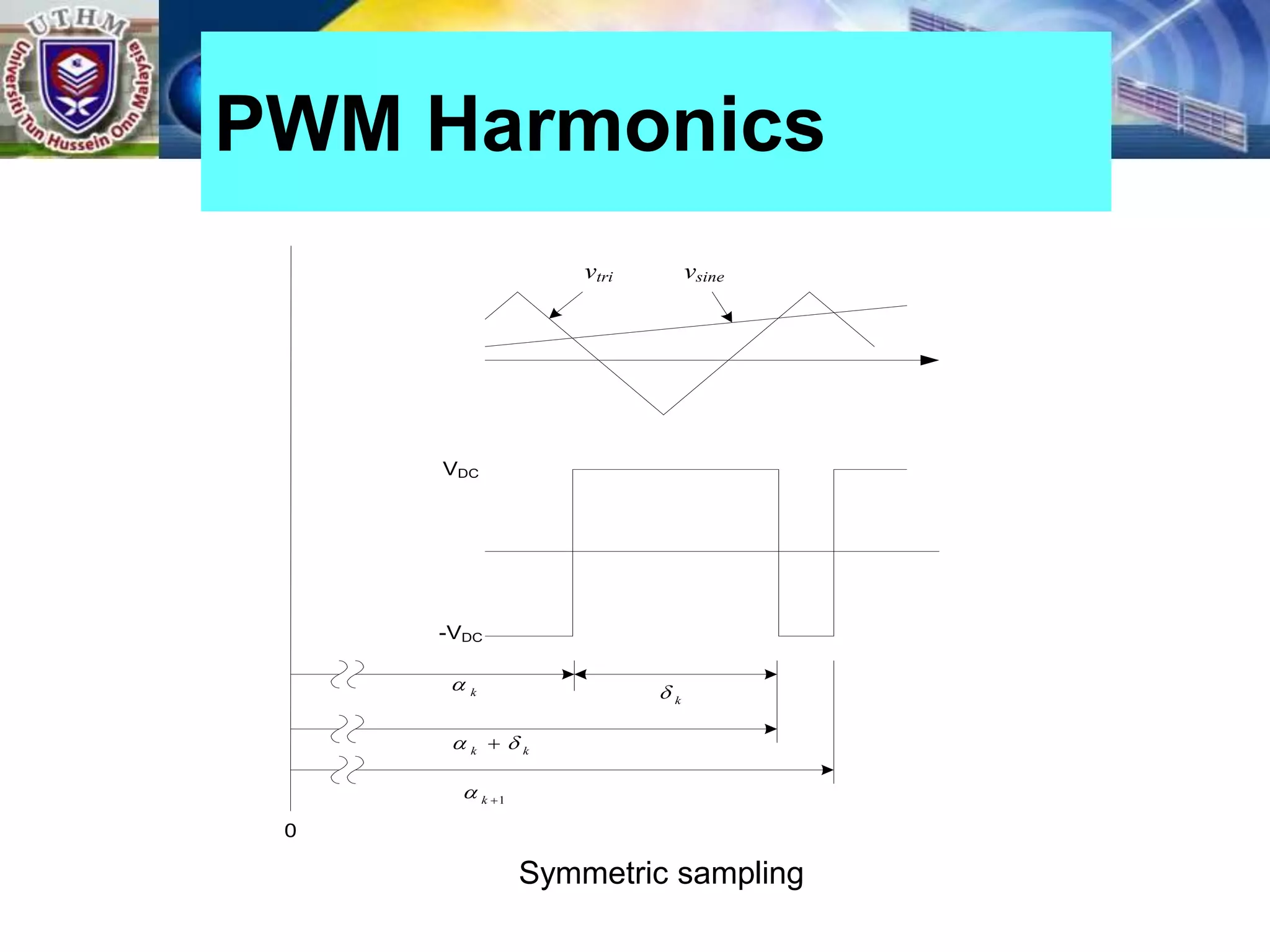
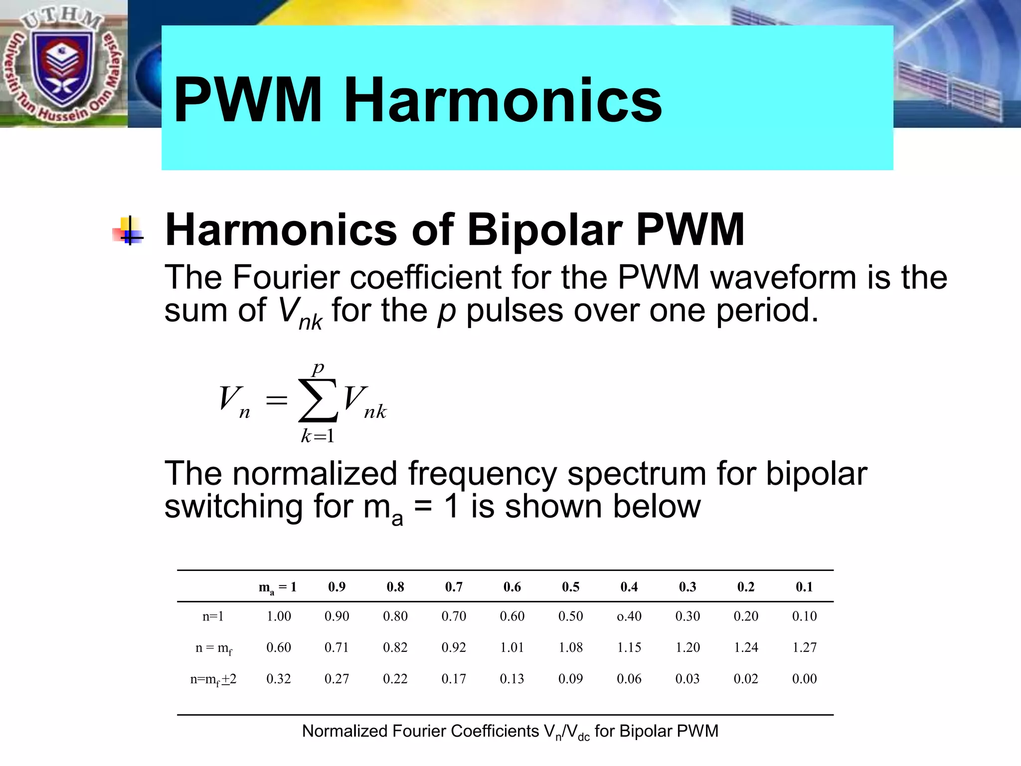
CHAPTER 4
INVERTERS:
Converting DC to AC
CONTENTS
۩ Introduction
۩ Basic Principles of Inverter
۩ Single-phase Half-Bridge Square-Wave Inverter
۩ Single-phase Full-Bridge Square-Wave Inverter
۩ Quasi Inverter
۩ Three-phase inverter
۩ Fourier Series and Harmonics Analysis
۩ Pulse-Width Modulation (PWM)
Definition:
Converts DC to AC power by switching the DC input
voltage in a pre-determined sequence so as to
generate AC voltage.
Applications:
Induction motor drives, traction, standby power
supplies, and uninterruptible ac power supplies (UPS).
INTRODUCTION
INTRODUCTION
Vdc Vac
+
-
+
-
General block diagram
Three types of inverter:
INTRODUCTION
Vdc Vac
+
-
+
-
AC
Load
Iac
Inverter
switching
control
“DC LINK”
Vdc
+
-
AC
Load
ILOAD
Inverter
switching
control
L
IDC
(a) Voltage source inverter (VSI) (b) Current source inverter (CSI)
Three types of inverter: (cont.)
INTRODUCTION
Vdc
+
-
AC
Load
Iac
Inverter
switching
control
Comparison
circuit
Reference
Waveform
Output current
sensing circuit
(c) Current regulated inverter
BASIC PRINCIPLES
The schematic of single-phase full-bridge square-wave
inverter circuit
D1
D2
D3
D4
T1 T3
T4 T2
+ V0 -
I0
VDC
BASIC PRINCIPLES
S1
S2
S3
+ V0 -
VDC
S4
V0
t1
VDC
t2
t
S1
S2
S3
+ V0 -
VDC
S4
V0
t3
-VDC
t2
t
Single-phase Half-bridge
Square-wave Inverter
V0
1
2
V0
G.
VDC
+
-
The basic single-phase half-bridge inverter circuit
 The total RMS value of the load output voltage,
 The instantaneous output voltage is: (refer to slide 30/pp:88)
 The fundamental rms output voltage (n=1)is
Single-phase Half-bridge
Square-wave Inverter
2
2
2 2
/
0
2
DC
T
DC
O
V
dt
V
T
V 
















 
2,4,....
n
for
0
sin
2
,...
5
,
3
,
1


 

n
DC
O t
n
n
V
v 

DC
DC
O V
V
V 45
.
0
2
1
2
1 








 In the case of RL load, the instantaneous load current io ,
where
 The fundamental output power is
Single-phase Half-bridge
Square-wave Inverter






,..
5
,
3
,
1
2
2
)
sin(
)
(
2
n
n
DC
o t
n
L
n
R
n
V
i 



)
/
(
tan 1
R
L
n
n 
 













2
2
2
1
1
1
1
1
)
(
2
2
cos
L
R
V
R
I
I
V
P
DC
o
o
o
o



 The total harmonic distortion (THD),
Single-phase Half-bridge
Square-wave Inverter






 

 ,....
7
,
5
,
3
2
1
1
n
n
O
V
V
THD
 
2
1
2
1
1
o
o
O
V
V
V
THD 

Example 3.1
The single-phase half-bridge inverter has a resistive load of R =
2.4Ω and the DC input voltage is 48V. Determine:
(a) the rms output voltage at the fundamental frequency
(b) the output power
(c) the average and peak current of each transistor.
(d) the THD
Single-phase Half-bridge
Square-wave Inverter
Solution
VDC = 48V and R = 2.4Ω
(a) The fundamental rms output voltage,
Vo1 = 0.45VDC = 0.45x48 = 21.6V
(b) For single-phase half-bridge inverter, the output voltage
Vo = VDC/2
Thus, the output power,
Single-phase Half-bridge
Square-wave Inverter
W
R
V
P o
o
240
4
.
2
)
2
/
48
(
/
2
2



Solution
(c) The transistor current Ip = 24/2.4 = 10 A
Because each of the transistor conducts for a 50% duty cycle,
the average current of each transistor is IQ = 10/2 = 5 A.
(d)
Single-phase Half-bridge
Square-wave Inverter
2
1
2
1
1
o
o
O
V
V
V
THD 

 
%
34
.
48
45
.
0
2
45
.
0
1 2
2








 DC
DC
DC
V
V
xV
 The switching in the second leg is delayed by 180
degrees from the first leg.
 The maximum output voltage of this inverter is twice
that of half-bridge inverter.
Single-phase Full-bridge
Square-wave Inverter
 The output RMS voltage
 And the instantaneous output voltage in a Fourier series is
 The fundamental RMS output voltage
 In the case of RL load, the instantaneous load current
Single-phase Full-bridge
Square-wave Inverter
DC
DC
O V
dt
V
T
V 






 
2
2



,...
5
,
3
,
1
sin
4
n
DC
O t
n
n
V
v 

DC
DC
V
V
V 9
.
0
2
4
1 


 
 
n
n
DC
o t
n
L
n
R
n
V
i 





 


sin
4
,...
5
,
3
,
1
2
2
Example 3.2
A single-phase full-bridge inverter with VDC = 230 and
consist of RLC in series. If R = 1.2Ω, ωL = 8 Ω and
1/ωC = 7 Ω, find:
(a) The amplitude of fundamental rms output current,
io1
(b) The fundamental component of output current in
function of time.
(c) The power delivered to the load due to the
fundamental component.
Single-phase Full-bridge
Square-wave Inverter
Example 3.3
A single-phase full-bridge inverter has an RLC load with R
= 10Ω, L = 31.5mH and C = 112μF. The inverter frequency
is 60Hz and the DC input voltage is 220V. Determine:
(a) Express the instantaneous load current in Fourier series.
(b) Calculate the rms load current at the fundamental
frequency.
(c) the THD of load current
(d) Power absorbed by the load and fundamental power.
(e) The average DC supply current and
(f) the rms and peak supply current of each transistor
Single-phase Full-bridge
Square-wave Inverter
Three-Phase Inverter
 Viewed as extensions of the single-phase bridge circuit.
 The switching signals for each switches of an inverter leg are
displaced or delayed by 120o.
 With 120o conduction, the switching pattern is T6T1 – T1T2 –
T2T3 – T3T4 – T4T5 – T5T6 – T6T1 for the positive A-B-C
sequence.
 When an upper switch in an inverter leg connected with the
positive DC rail is turned ON, the output terminal of the leg
(phase voltage) goes to potential +VDC/2.
 When a lower switch in an inverter leg connected with the
negative DC rail is turned ON, the output terminal of that leg
(phase voltage) goes to potential -VDC/2.
Three-Phase Inverter
 The line-to-neutral voltage can be expressed in Fourier series
 The line voltage is vab = √3van with phase advance of 30o
Three-Phase Inverter

































,..
5
,
3
,
1
,..
5
,
3
,
1
,..
5
,
3
,
1
6
7
sin
3
sin
2
2
sin
3
sin
2
6
sin
3
sin
2
n
dc
cn
n
dc
bn
n
dc
an
t
n
n
n
V
v
t
n
n
n
V
v
t
n
n
n
V
v












 



























,..
5
,
3
,
1
,..
5
,
3
,
1
,..
5
,
3
,
1
sin
3
sin
3
2
3
sin
3
sin
3
2
3
sin
3
sin
3
2
n
dc
ca
n
dc
bc
n
dc
ab
t
n
n
n
V
v
t
n
n
n
V
v
t
n
n
n
V
v












 Fourier series is a tool to analyze the wave shapes of the
output voltage and current in terms of Fourier series.
Fourier Series and
Harmonics Analysis
 





2
0
1
d
v
f
ao
   






2
0
cos
1
d
n
v
f
an
   






2
0
sin
1
d
n
v
f
bn
Inverse Fourier
   






1
0 sin
cos
2
1
n
n n
bn
n
a
a
v
f 

Where
t

 
 If no DC component in the output, the output voltage and
current are
 The rms current of the load can be determined by
Fourier Series and
Harmonics Analysis
 





1
sin
)
(
n
n
n
o t
n
V
t
v 

 





1
sin
)
(
n
n
n
o t
n
I
t
i 

2
1
1
2
,
2














n
n
n
rms
n
rms
I
I
I
Where
n
n
n
Z
V
I 
 The total power absorbed in the load resistor can be
determined by
Fourier Series and
Harmonics Analysis








1
2
,
1 n
rms
n
n
n R
I
P
P
 Since the objective of the inverter is to use a
DC voltage source to supply a load that
requiring AC voltage, hence the quality of
the non-sinusoidal AC output voltage or
current can be expressed in terms of THD.
 The harmonics is considered to ensure that
the quality of the waveform must match to
the utility supply which means of power
quality issues.
 This is due to the harmonics may cause
degradation of the equipments and needs to
be de-rated.
Total Harmonics
Distortion
Total Harmonics
Distortion
 The THD of the load voltage is expressed as,
 The current THD can be obtained by replacing the
harmonic voltage with harmonic current,
Total Harmonics
Distortion
rms
rms
rms
rms
n rms
n
v
V
V
V
V
V
THD
,
1
2
,
1
2
,
1
2
2
, )
( 





rms
n rms
n
i
I
I
THD
,
1
2
2
, )
(




Harmonics of Square-
wave Waveform

2

t

 
DC
V
DC
V

0
1
0
2
0 








  
 


 DC
DC V
d
V
a
0
)
cos(
)
cos(
0
2








  
 






d
n
d
n
V
a DC
n
 
 
 
 


















 

n
n
n
n
n
n
V
n
n
n
V
d
n
d
n
V
b
DC
DC
DC
n
cos
1
2
)
cos
2
(cos
)
cos
0
(cos
)
cos(
)
cos(
)
sin(
)
sin(
2
0
0
2
















  
 When the harmonics number, n of a waveform is
even number, the resultant of
Therefore,
 When n is odd number,
Hence,
Harmonics of Square-wave
Waveform
1
cos 

n
0

n
b
1
cos 


n

n
V
b DC
n
4

Spectrum of Square-
wave
Normalised
Fundamental
1st
3rd
5th
7th
9th
11th
n
(0.33)
(0.2)
(0.14)
(0.11)
(0.09)
• Harmonic decreases with
a factor of (1/n).
• Even harmonics are
absent
• Nearest harmonics is the
3rd. If fundamental is
50Hz, then nearest
harmonic is 150Hz.
• Due to the small
separation between the
fundamental and 3rd
harmonics, output low-
pass filter design can be
very difficult.
Quasi-square wave
an = 0, due to half-wave symmetry
Quasi-square wave
Therefore,
If n is even, bn = 0;
If n is odd, 

cos
4
n
V
b dc
n 
Example 3.4
The full-bridge inverter with DC input voltage of 100V,
load resistor and inductor of 10Ω and 25mH
respectively and operated at 60 Hz frequency.
Determine:
(a) The amplitude of the Fourier series terms for the
square-wave load voltage.
(b) The amplitude of the Fourier series terms for load
current.
(c) Power absorbed by the load.
(d) The THD of the load voltage and load current for
square-wave inverter.
Amplitude and
Harmonics Control
 
2
t

VDC
-VDC
   
S2
S4
S1
S2
S1
S3
S3
S4
S2
S4
0 VDC 0 0
-VDC
S1 Closed Opened
S2
S3
S4
Vo
The output voltage of the full-
bridge inverter can be controlled
by adjusting the interval of on
each side of the pulse as zero .
The rms value of the voltage waveform is
The Fourier series of the waveform is expressed as
The amplitude of half-wave symmetry is
Amplitude and
Harmonics Control







2
1
)
(
1 2


 

DC
DC
rms V
t
d
V
V


odd
n
n
O t
n
V
t
v
,
)
sin(
)
( 
)
cos(
4
)
(
)
sin(
2








n
n
V
t
d
t
n
V
V DC
DC
n 






 

The amplitude of the fundamental frequency is controllable by
adjusting the angle of α.
The nth harmonic can be eliminated by proper choice of
displacement angle α if
Amplitude and
Harmonics Control


cos
4
1 





 DC
V
V
0
cos 

n
OR
n

90


 Pulse-width modulation provides a way to decrease
the total harmonics distortion (THD).
 Types of PWM scheme
 Natural or sinusoidal sampling
 Regular sampling
 Optimize PWM
 Harmonic elimination/minimization PWM
 SVM
Pulse-Width Modulation
(PWM)
 Several definition in PWM
(i) Amplitude Modulation, Ma
If Ma ≤ 1, the amplitude of the fundamental
frequency of the output voltage, V1 is linearly
proportional to Ma.
(ii) Frequency Modulation, Mf
Pulse-Width Modulation
(PWM)
tri
,
sin
,
carrier
,
,
m
e
m
m
reference
m
a
V
V
V
V
M 

e
tri
carrier
f
f
f
f
f
M
sin
reference


Bipolar Switching of PWM
Pulse-Width Modulation
(PWM)
vtri (carrier)
vsine (reference)
VDC
-VDC
(a)
(b)
S1 and S2 ON when Vsine > Vtri
S3 and S4 ON when Vsine < Vtri
Sinusoidal PWM Generator -Bipolar
Pulse-Width Modulation
(PWM)
G1, G2
G3, G4
Unipolar Switching
of PWM
Pulse-Width Modulation
(PWM)
vtri (carrier)
vsine (reference)
(a)
(b)
(c)
S4
S2
Vo
Vdc
0
Vdc
0
S1 is ON when Vsine > Vtri
S2 is ON when –Vsine < Vtri
S3 is ON when –Vsine > Vtri
S4 is ON when Vsine < Vtri
Sinusoidal
PWM
Generator-
Unipolar
■ Advantages of PWM switching
- provides a way to decrease the THD of load current.
- the amplitude of the o/p voltage can be controlled with the
modulating waveform.
- reduced filter requirements to decrease harmonics.
■ Disadvantages of PWM switching
- complex control circuit for the switches
- increase losses due to more frequent switching.
Pulse-Width Modulation
(PWM)
Harmonics of Bipolar PWM
Assuming the PWM output is symmetry, the
harmonics of each kth PWM pulse can be
expressed
Finally, the resultant of the integration is
PWM Harmonics





 


 




k
k
k k
k
t
d
t
n
-V
t
d
t
n
V
t
d
t
n
t
v
V
DC
DC
T
nk














1
k
)
(
)
sin(
)
(
)
(
)
sin(
2
)
(
)
sin(
)
(
2
0
 
)
(
cos
2
cos
cos
2
1 k
k
k
k
DC
nk n
n
n
n
V
V 







 
PWM Harmonics
vtri vsine
VDC
-VDC
k

k
k

 
1

k

k

0
Symmetric sampling
Harmonics of Bipolar PWM
The Fourier coefficient for the PWM waveform is the
sum of Vnk for the p pulses over one period.
The normalized frequency spectrum for bipolar
switching for ma = 1 is shown below
PWM Harmonics



p
k
nk
n V
V
1
ma = 1 0.9 0.8 0.7 0.6 0.5 0.4 0.3 0.2 0.1
n=1 1.00 0.90 0.80 0.70 0.60 0.50 o.40 0.30 0.20 0.10
n = mf 0.60 0.71 0.82 0.92 1.01 1.08 1.15 1.20 1.24 1.27
n=mf +2 0.32 0.27 0.22 0.17 0.13 0.09 0.06 0.03 0.02 0.00
Normalized Fourier Coefficients Vn/Vdc for Bipolar PWM
Example 3.5
The inverter has a resistive load of 10Ω and
inductive load of 25mH connected in series with
the fundamental frequency current amplitude of
9.27A. The THD of the inverter is not more than
10%. If at the beginning of designing the inverter,
the THD of the current is 16.7% which is does
not meet the specification, find the voltage
amplitude at the fundamental frequency, the
required DC input supply and the new THD of the
current.
Example 3.6
The single-phase full-bridge inverter is used to produce
a 60Hz voltage across a series R-L load using bipolar
PWM. The DC input to the bridge is 100V, the
amplitude modulation ratio is 0.8, and the frequency
modulation ratio is 21. The load has resistance of R =
10Ω and inductance L = 20mH. Determine:
(a) The amplitude of the 60Hz component of the output
voltage and load current.
(b) The power absorbed by the load resistor
(c) The THD of the load current

chapter4 DC to AC Converter.ppt

  • 1.
  • 2.
    CONTENTS ۩ Introduction ۩ BasicPrinciples of Inverter ۩ Single-phase Half-Bridge Square-Wave Inverter ۩ Single-phase Full-Bridge Square-Wave Inverter ۩ Quasi Inverter ۩ Three-phase inverter ۩ Fourier Series and Harmonics Analysis ۩ Pulse-Width Modulation (PWM)
  • 3.
    Definition: Converts DC toAC power by switching the DC input voltage in a pre-determined sequence so as to generate AC voltage. Applications: Induction motor drives, traction, standby power supplies, and uninterruptible ac power supplies (UPS). INTRODUCTION
  • 4.
  • 5.
    Three types ofinverter: INTRODUCTION Vdc Vac + - + - AC Load Iac Inverter switching control “DC LINK” Vdc + - AC Load ILOAD Inverter switching control L IDC (a) Voltage source inverter (VSI) (b) Current source inverter (CSI)
  • 6.
    Three types ofinverter: (cont.) INTRODUCTION Vdc + - AC Load Iac Inverter switching control Comparison circuit Reference Waveform Output current sensing circuit (c) Current regulated inverter
  • 7.
    BASIC PRINCIPLES The schematicof single-phase full-bridge square-wave inverter circuit D1 D2 D3 D4 T1 T3 T4 T2 + V0 - I0 VDC
  • 8.
    BASIC PRINCIPLES S1 S2 S3 + V0- VDC S4 V0 t1 VDC t2 t S1 S2 S3 + V0 - VDC S4 V0 t3 -VDC t2 t
  • 9.
    Single-phase Half-bridge Square-wave Inverter V0 1 2 V0 G. VDC + - Thebasic single-phase half-bridge inverter circuit
  • 10.
     The totalRMS value of the load output voltage,  The instantaneous output voltage is: (refer to slide 30/pp:88)  The fundamental rms output voltage (n=1)is Single-phase Half-bridge Square-wave Inverter 2 2 2 2 / 0 2 DC T DC O V dt V T V                    2,4,.... n for 0 sin 2 ,... 5 , 3 , 1      n DC O t n n V v   DC DC O V V V 45 . 0 2 1 2 1         
  • 11.
     In thecase of RL load, the instantaneous load current io , where  The fundamental output power is Single-phase Half-bridge Square-wave Inverter       ,.. 5 , 3 , 1 2 2 ) sin( ) ( 2 n n DC o t n L n R n V i     ) / ( tan 1 R L n n                 2 2 2 1 1 1 1 1 ) ( 2 2 cos L R V R I I V P DC o o o o   
  • 12.
     The totalharmonic distortion (THD), Single-phase Half-bridge Square-wave Inverter           ,.... 7 , 5 , 3 2 1 1 n n O V V THD   2 1 2 1 1 o o O V V V THD  
  • 13.
    Example 3.1 The single-phasehalf-bridge inverter has a resistive load of R = 2.4Ω and the DC input voltage is 48V. Determine: (a) the rms output voltage at the fundamental frequency (b) the output power (c) the average and peak current of each transistor. (d) the THD Single-phase Half-bridge Square-wave Inverter
  • 14.
    Solution VDC = 48Vand R = 2.4Ω (a) The fundamental rms output voltage, Vo1 = 0.45VDC = 0.45x48 = 21.6V (b) For single-phase half-bridge inverter, the output voltage Vo = VDC/2 Thus, the output power, Single-phase Half-bridge Square-wave Inverter W R V P o o 240 4 . 2 ) 2 / 48 ( / 2 2   
  • 15.
    Solution (c) The transistorcurrent Ip = 24/2.4 = 10 A Because each of the transistor conducts for a 50% duty cycle, the average current of each transistor is IQ = 10/2 = 5 A. (d) Single-phase Half-bridge Square-wave Inverter 2 1 2 1 1 o o O V V V THD     % 34 . 48 45 . 0 2 45 . 0 1 2 2          DC DC DC V V xV
  • 16.
     The switchingin the second leg is delayed by 180 degrees from the first leg.  The maximum output voltage of this inverter is twice that of half-bridge inverter. Single-phase Full-bridge Square-wave Inverter
  • 17.
     The outputRMS voltage  And the instantaneous output voltage in a Fourier series is  The fundamental RMS output voltage  In the case of RL load, the instantaneous load current Single-phase Full-bridge Square-wave Inverter DC DC O V dt V T V          2 2    ,... 5 , 3 , 1 sin 4 n DC O t n n V v   DC DC V V V 9 . 0 2 4 1        n n DC o t n L n R n V i           sin 4 ,... 5 , 3 , 1 2 2
  • 18.
    Example 3.2 A single-phasefull-bridge inverter with VDC = 230 and consist of RLC in series. If R = 1.2Ω, ωL = 8 Ω and 1/ωC = 7 Ω, find: (a) The amplitude of fundamental rms output current, io1 (b) The fundamental component of output current in function of time. (c) The power delivered to the load due to the fundamental component. Single-phase Full-bridge Square-wave Inverter
  • 19.
    Example 3.3 A single-phasefull-bridge inverter has an RLC load with R = 10Ω, L = 31.5mH and C = 112μF. The inverter frequency is 60Hz and the DC input voltage is 220V. Determine: (a) Express the instantaneous load current in Fourier series. (b) Calculate the rms load current at the fundamental frequency. (c) the THD of load current (d) Power absorbed by the load and fundamental power. (e) The average DC supply current and (f) the rms and peak supply current of each transistor Single-phase Full-bridge Square-wave Inverter
  • 20.
  • 21.
     Viewed asextensions of the single-phase bridge circuit.  The switching signals for each switches of an inverter leg are displaced or delayed by 120o.  With 120o conduction, the switching pattern is T6T1 – T1T2 – T2T3 – T3T4 – T4T5 – T5T6 – T6T1 for the positive A-B-C sequence.  When an upper switch in an inverter leg connected with the positive DC rail is turned ON, the output terminal of the leg (phase voltage) goes to potential +VDC/2.  When a lower switch in an inverter leg connected with the negative DC rail is turned ON, the output terminal of that leg (phase voltage) goes to potential -VDC/2. Three-Phase Inverter
  • 23.
     The line-to-neutralvoltage can be expressed in Fourier series  The line voltage is vab = √3van with phase advance of 30o Three-Phase Inverter                                  ,.. 5 , 3 , 1 ,.. 5 , 3 , 1 ,.. 5 , 3 , 1 6 7 sin 3 sin 2 2 sin 3 sin 2 6 sin 3 sin 2 n dc cn n dc bn n dc an t n n n V v t n n n V v t n n n V v                                          ,.. 5 , 3 , 1 ,.. 5 , 3 , 1 ,.. 5 , 3 , 1 sin 3 sin 3 2 3 sin 3 sin 3 2 3 sin 3 sin 3 2 n dc ca n dc bc n dc ab t n n n V v t n n n V v t n n n V v            
  • 24.
     Fourier seriesis a tool to analyze the wave shapes of the output voltage and current in terms of Fourier series. Fourier Series and Harmonics Analysis        2 0 1 d v f ao           2 0 cos 1 d n v f an           2 0 sin 1 d n v f bn Inverse Fourier           1 0 sin cos 2 1 n n n bn n a a v f   Where t   
  • 25.
     If noDC component in the output, the output voltage and current are  The rms current of the load can be determined by Fourier Series and Harmonics Analysis        1 sin ) ( n n n o t n V t v          1 sin ) ( n n n o t n I t i   2 1 1 2 , 2               n n n rms n rms I I I Where n n n Z V I 
  • 26.
     The totalpower absorbed in the load resistor can be determined by Fourier Series and Harmonics Analysis         1 2 , 1 n rms n n n R I P P
  • 27.
     Since theobjective of the inverter is to use a DC voltage source to supply a load that requiring AC voltage, hence the quality of the non-sinusoidal AC output voltage or current can be expressed in terms of THD.  The harmonics is considered to ensure that the quality of the waveform must match to the utility supply which means of power quality issues.  This is due to the harmonics may cause degradation of the equipments and needs to be de-rated. Total Harmonics Distortion
  • 28.
  • 29.
     The THDof the load voltage is expressed as,  The current THD can be obtained by replacing the harmonic voltage with harmonic current, Total Harmonics Distortion rms rms rms rms n rms n v V V V V V THD , 1 2 , 1 2 , 1 2 2 , ) (       rms n rms n i I I THD , 1 2 2 , ) (    
  • 30.
    Harmonics of Square- waveWaveform  2  t    DC V DC V  0 1 0 2 0                  DC DC V d V a 0 ) cos( ) cos( 0 2                    d n d n V a DC n                              n n n n n n V n n n V d n d n V b DC DC DC n cos 1 2 ) cos 2 (cos ) cos 0 (cos ) cos( ) cos( ) sin( ) sin( 2 0 0 2                   
  • 31.
     When theharmonics number, n of a waveform is even number, the resultant of Therefore,  When n is odd number, Hence, Harmonics of Square-wave Waveform 1 cos   n 0  n b 1 cos    n  n V b DC n 4 
  • 32.
    Spectrum of Square- wave Normalised Fundamental 1st 3rd 5th 7th 9th 11th n (0.33) (0.2) (0.14) (0.11) (0.09) •Harmonic decreases with a factor of (1/n). • Even harmonics are absent • Nearest harmonics is the 3rd. If fundamental is 50Hz, then nearest harmonic is 150Hz. • Due to the small separation between the fundamental and 3rd harmonics, output low- pass filter design can be very difficult.
  • 33.
    Quasi-square wave an =0, due to half-wave symmetry
  • 34.
    Quasi-square wave Therefore, If nis even, bn = 0; If n is odd,   cos 4 n V b dc n 
  • 35.
    Example 3.4 The full-bridgeinverter with DC input voltage of 100V, load resistor and inductor of 10Ω and 25mH respectively and operated at 60 Hz frequency. Determine: (a) The amplitude of the Fourier series terms for the square-wave load voltage. (b) The amplitude of the Fourier series terms for load current. (c) Power absorbed by the load. (d) The THD of the load voltage and load current for square-wave inverter.
  • 36.
    Amplitude and Harmonics Control  2 t  VDC -VDC     S2 S4 S1 S2 S1 S3 S3 S4 S2 S4 0 VDC 0 0 -VDC S1 Closed Opened S2 S3 S4 Vo The output voltage of the full- bridge inverter can be controlled by adjusting the interval of on each side of the pulse as zero .
  • 37.
    The rms valueof the voltage waveform is The Fourier series of the waveform is expressed as The amplitude of half-wave symmetry is Amplitude and Harmonics Control        2 1 ) ( 1 2      DC DC rms V t d V V   odd n n O t n V t v , ) sin( ) (  ) cos( 4 ) ( ) sin( 2         n n V t d t n V V DC DC n          
  • 38.
    The amplitude ofthe fundamental frequency is controllable by adjusting the angle of α. The nth harmonic can be eliminated by proper choice of displacement angle α if Amplitude and Harmonics Control   cos 4 1        DC V V 0 cos   n OR n  90  
  • 39.
     Pulse-width modulationprovides a way to decrease the total harmonics distortion (THD).  Types of PWM scheme  Natural or sinusoidal sampling  Regular sampling  Optimize PWM  Harmonic elimination/minimization PWM  SVM Pulse-Width Modulation (PWM)
  • 40.
     Several definitionin PWM (i) Amplitude Modulation, Ma If Ma ≤ 1, the amplitude of the fundamental frequency of the output voltage, V1 is linearly proportional to Ma. (ii) Frequency Modulation, Mf Pulse-Width Modulation (PWM) tri , sin , carrier , , m e m m reference m a V V V V M   e tri carrier f f f f f M sin reference  
  • 41.
    Bipolar Switching ofPWM Pulse-Width Modulation (PWM) vtri (carrier) vsine (reference) VDC -VDC (a) (b) S1 and S2 ON when Vsine > Vtri S3 and S4 ON when Vsine < Vtri
  • 42.
    Sinusoidal PWM Generator-Bipolar Pulse-Width Modulation (PWM) G1, G2 G3, G4
  • 43.
    Unipolar Switching of PWM Pulse-WidthModulation (PWM) vtri (carrier) vsine (reference) (a) (b) (c) S4 S2 Vo Vdc 0 Vdc 0 S1 is ON when Vsine > Vtri S2 is ON when –Vsine < Vtri S3 is ON when –Vsine > Vtri S4 is ON when Vsine < Vtri
  • 44.
  • 45.
    ■ Advantages ofPWM switching - provides a way to decrease the THD of load current. - the amplitude of the o/p voltage can be controlled with the modulating waveform. - reduced filter requirements to decrease harmonics. ■ Disadvantages of PWM switching - complex control circuit for the switches - increase losses due to more frequent switching. Pulse-Width Modulation (PWM)
  • 46.
    Harmonics of BipolarPWM Assuming the PWM output is symmetry, the harmonics of each kth PWM pulse can be expressed Finally, the resultant of the integration is PWM Harmonics                k k k k k t d t n -V t d t n V t d t n t v V DC DC T nk               1 k ) ( ) sin( ) ( ) ( ) sin( 2 ) ( ) sin( ) ( 2 0   ) ( cos 2 cos cos 2 1 k k k k DC nk n n n n V V          
  • 47.
    PWM Harmonics vtri vsine VDC -VDC k  k k   1  k  k  0 Symmetric sampling
  • 48.
    Harmonics of BipolarPWM The Fourier coefficient for the PWM waveform is the sum of Vnk for the p pulses over one period. The normalized frequency spectrum for bipolar switching for ma = 1 is shown below PWM Harmonics    p k nk n V V 1 ma = 1 0.9 0.8 0.7 0.6 0.5 0.4 0.3 0.2 0.1 n=1 1.00 0.90 0.80 0.70 0.60 0.50 o.40 0.30 0.20 0.10 n = mf 0.60 0.71 0.82 0.92 1.01 1.08 1.15 1.20 1.24 1.27 n=mf +2 0.32 0.27 0.22 0.17 0.13 0.09 0.06 0.03 0.02 0.00 Normalized Fourier Coefficients Vn/Vdc for Bipolar PWM
  • 49.
    Example 3.5 The inverterhas a resistive load of 10Ω and inductive load of 25mH connected in series with the fundamental frequency current amplitude of 9.27A. The THD of the inverter is not more than 10%. If at the beginning of designing the inverter, the THD of the current is 16.7% which is does not meet the specification, find the voltage amplitude at the fundamental frequency, the required DC input supply and the new THD of the current.
  • 50.
    Example 3.6 The single-phasefull-bridge inverter is used to produce a 60Hz voltage across a series R-L load using bipolar PWM. The DC input to the bridge is 100V, the amplitude modulation ratio is 0.8, and the frequency modulation ratio is 21. The load has resistance of R = 10Ω and inductance L = 20mH. Determine: (a) The amplitude of the 60Hz component of the output voltage and load current. (b) The power absorbed by the load resistor (c) The THD of the load current