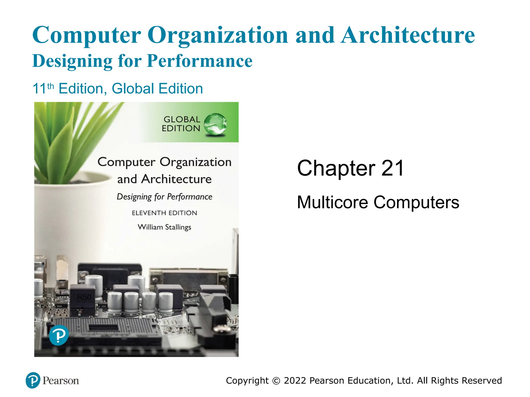
#2 The organizational changes in processor design have primarily been focused on
exploiting ILP, so that more work is done in each clock cycle. These changes include,
in chronological order (Figure 21.1):
* Pipelining: Individual instructions are executed through a pipeline of stages so that while one instruction is executing in one stage of the pipeline, another instruction is executing in another stage of the pipeline.
* Superscalar: Multiple pipelines are constructed by replicating execution resources. This enables parallel execution of instructions in parallel pipelines, so long as hazards are avoided.
Simultaneous multithreading (SMT): Register banks are replicated so that multiple threads can share the use of pipeline resources.
With each of these innovations, designers have over the years attempted to
increase the performance of the system by adding complexity. In the case of pipelining,
simple three-stage pipelines were replaced by pipelines with five stages. Intel’s
Pentium 4 “Prescott” core had 31 stages for some instructions.
There is a practical limit to how far this trend can be taken, because with more
stages, there is the need for more logic, more interconnections, and more control signals.
With superscalar organization, increased performance can be achieved by
increasing the number of parallel pipelines. Again, there are diminishing returns
as the number of pipelines increases. More logic is required to manage hazards and
to stage instruction resources. Eventually, a single thread of execution reaches the
point where hazards and resource dependencies prevent the full use of the multiple
pipelines available. Also, compiled binary code rarely exposes enough ILP to take
advantage of more than about six parallel pipelines.
This same point of diminishing returns is reached with SMT, as the complexity
of managing multiple threads over a set of pipelines limits the number of threads
and number of pipelines that can be effectively utilized. SMT’s advantage lies in the
fact that two (or more) program streams can be searched for available ILP.
There is a related set of problems dealing with the design and fabrication of
the computer chip. The increase in complexity to deal with all of the logical issues
related to very long pipelines, multiple superscalar pipelines, and multiple SMT
register banks means that increasing amounts of the chip area are occupied with
coordinating and signal transfer logic. This increases the difficulty of designing, fabricating,
and debugging the chips. The increasingly difficult engineering challenge
related to processor logic is one of the reasons that an increasing fraction of the
processor chip is devoted to the simpler memory logic. Power issues, discussed next,
provide another reason.
#3 To maintain the trend of higher performance as the number of transistors per chip
rises, designers have resorted to more elaborate processor designs (pipelining, superscalar,
SMT) and to high clock frequencies. Unfortunately, power requirements have
grown exponentially as chip density and clock frequency have risen. This was shown
in Figure 2.2.
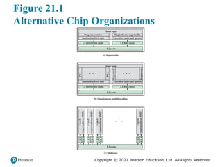
One way to control power density is to use more of the chip area for cache
memory. Memory transistors are smaller and have a power density an order of
magnitude lower than that of logic (see Figure 21.2). As chip transistor density has
increased, the percentage of chip area devoted to memory has grown, and is now
often half the chip area. Even so, there is still a considerable amount of chip area
devoted to processing logic.
How to use all those logic transistors is a key design issue. As discussed earlier
in this section, there are limits to the effective use of such techniques as superscalar
and SMT. In general terms, the experience of recent decades has been encapsulated
in a rule of thumb known as Pollack’s rule [POLL99], which states that performance
increase is roughly proportional to square root of increase in complexity.
In other words, if you double the logic in a processor core, then it delivers only
40% more performance. In principle, the use of multiple cores has the potential to
provide near-linear performance improvement with the increase in the number of
cores—but only for software that can take advantage.
Power considerations provide another motive for moving toward a multicore
organization. Because the chip has such a huge amount of cache memory,
it becomes unlikely that any one thread of execution can effectively use all that
memory. Even with SMT, multithreading is done in a relatively limited fashion and
cannot therefore fully exploit a gigantic cache, whereas a number of relatively independent
threads or processes has a greater opportunity to take full advantage of the
cache memory.
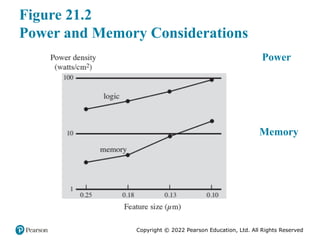
#4 The potential performance benefits of a multicore organization depend on the ability to effectively exploit the parallel resources available to the application. Let us focus first on a single application running on a multicore system.
The law assumes a program in which a fraction (1 – f ) of the execution time involves code that is inherently serial and a fraction f that involves code that is infinitely parallelizable with no scheduling overhead.
This law appears to make the prospect of a multicore organization attractive. But as Figure 21.3a shows, even a small amount of serial code has a noticeable impact. If only 10% of the code is inherently serial (f = 0.9), running the program on a multi- core system with 8 processors yields a performance gain of only a factor of 4.7. In addition, software typically incurs overhead as a result of communication and distribution of work among multiple processors and as a result of cache coherence overhead. This results in a curve where performance peaks and then begins to degrade because of the increased burden of the overhead of using multiple processors (e.g., coordination and OS management). Figure 21.3b, from [MCDO05], is a representative example.
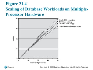
#5 However, software engineers have been addressing this problem and there are numerous applications in which it is possible to effectively exploit a multicore sys- tem. [MCDO05] analyzes the effectiveness of multicore systems on a set of database applications, in which great attention was paid to reducing the serial fraction within hardware architectures, operating systems, middleware, and the database application software. Figure 21.4 shows the result. As this example shows, database management systems and database applications are one area in which multicore systems can be used effectively. Many kinds of servers can also effectively use the parallel multicore organization, because servers typically handle numerous relatively independent transactions in parallel.
#6 In addition to general-purpose server software, a number of classes of applications benefit directly from the ability to scale throughput with the number of cores. [MCDO06] lists the following examples:
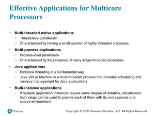
■ Multithreaded native applications (thread-level parallelism): Multithreaded
applications are characterized by having a small number of highly threaded
processes.
■ Multiprocess applications (process-level parallelism): Multiprocess applications
are characterized by the presence of many single-threaded processes.
■ Java applications: Java applications embrace threading in a fundamental way.
Not only does the Java language greatly facilitate multithreaded applications,
but the Java Virtual Machine is a multithreaded process that provides scheduling
and memory management for Java applications.
■ Multi-instance applications (application-level parallelism): Even if an individual
application does not scale to take advantage of a large number of threads,
it is still possible to gain from multicore architecture by running multiple
instances of the application in parallel. If multiple application instances
require some degree of isolation, virtualization technology (for the hardware
of the operating system) can be used to provide each of them with its own
separate and secure domain.
#7 Before turning to an example, we elaborate on the topic of thread-level
parallelism by introducing the concept of threading granularity , which can be defined
as the minimal unit of work that can be beneficially parallelized. In general, the
finer the granularity the system enables, the less constrained is the programmer in
parallelizing a program. Consequently, finer grain threading systems allow parallelization
in more situations than coarse-grained ones. The choice of the target granularity
of an architecture involves an inherent tradeoff. On the one hand, the finer
grain systems are preferable because of the flexibility they afford to the programmer.
On the other hand, the finer the threading granularity, the more significant
part of the execution is taken by the threading system overhead.
#8 Valve is an entertainment and technology company that has developed a number of popular games, as well as the Source engine, one of the most widely played game engines available. Source is an animation engine used by Valve for its games and licensed for other game developers.
Valve has reprogrammed the Source engine software to use multithreading to exploit the power of multicore processor chips from Intel and AMD [REIM06]. The revised Source engine code provides more powerful support for Valve games such as Half Life 2.
Valve found that through coarse threading, it could achieve up to twice the performance across two processors compared to executing on a single processor. But this performance gain could only be achieved with contrived cases. For real- world gameplay, the improvement was on the order of a factor of 1.2. Valve also found that effective use of fine-grain threading was difficult. The time per work unit can be variable, and managing the timeline of outcomes and consequences involved complex programming.
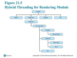
Valve found that a hybrid threading approach was the most promising and would scale the best as multicore systems with eight or sixteen processors became available. Valve identified systems that operate very effectively when assigned to a single processor permanently. An example is sound mixing, which has little user interaction, is not constrained by the frame configuration of windows, and works on its own set of data. Other modules, such as scene rendering, can be organized into a number of threads so that the module can execute on a single processor but achieve greater performance as it is spread out over more and more processors.
Figure 21.5 illustrates the thread structure for the rendering module. In this hierarchical structure, higher-level threads spawn lower-level threads as needed. The rendering module relies on a critical part of the Source engine, the world list, which is a database representation of the visual elements in the game’s world. The first task is to determine what are the areas of the world that need to be rendered. The next task is to determine what objects are in the scene as viewed from multiple angles. Then comes the processor-intensive work. The rendering module has to work out the rendering of each object from multiple points of view, such as the player’s view, the view of TV monitors, and the point of view of reflections in water.
Some of the key elements of the threading strategy for the rendering module are listed in [LEON07] and include the following:
• Construct scene-rendering lists for multiple scenes in parallel (e.g., the world and its reflection in water).
• Overlap graphics simulation.
* Compute character bone transformations for all characters in all scenes in
parallel.
* Allow multiple threads to draw in parallel.
The designers found that simply locking key databases, such as the world list, for a thread was too inefficient. Over 95% of the time, a thread is trying to read from a data set, and only 5% of the time at most is spent in writing to a data set. Thus, a concurrency mechanism known as the single-writer-multiple-readers model works effectively.
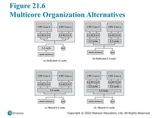
#9 Figure 21.6 shows four general organizations for multicore systems. Figure 21.6a is an organization found in some of the earlier multicore computer chips and is still seen in embedded chips. In this organization, the only on-chip cache is L1 cache, with each core having its own dedicated L1 cache. Almost invariably, the L1 cache is divided into instruction and data caches. An example of this organization is the ARM11 MPCore.
The organization of Figure 21.6b is also one in which there is no on-chip cache
sharing. In this, there is enough area available on the chip to allow for L2 cache.
An example of this organization is the AMD Opteron. Figure 21.6c shows a similar
allocation of chip space to memory, but with the use of a shared L2 cache. The Intel
Core Duo has this organization. Finally, as the amount of cache memory available
on the chip continues to grow, performance considerations dictate splitting off a
separate, shared L3 cache (Figure 21.6d), with dedicated L1 and L2 caches for each
core processor. The Intel Core i7 is an example of this organization.
The use of a shared higher-level cache on the chip has several advantages over
exclusive reliance on dedicated caches:
1. Constructive interference can reduce overall miss rates. That is, if a thread on
one core accesses a main memory location, this brings the line containing the
referenced location into the shared cache. If a thread on another core soon
thereafter accesses the same memory block, the memory locations will already
be available in the shared on-chip cache.
2. A related advantage is that data shared by multiple cores is not replicated at
the shared cache level.
3. With proper line replacement algorithms, the amount of shared cache allocated
to each core is dynamic, so that threads that have less locality (larger
working sets) can employ more cache.
4. Inter-core communication is easy to implement, via shared memory locations.
5. The use of a shared higher-level cache confines the cache coherency problem
to the lower cache levels, which may provide some additional performance
advantage.
A potential advantage to having only dedicated L2 caches on the chip is that
each core enjoys more rapid access to its private L2 cache. This is advantageous for
threads that exhibit strong locality.
As both the amount of memory available and the number of cores grow, the
use of a shared L3 cache combined with dedicated percore L2 caches in Figure 21.6d
seems likely to provide better performance than simply a massive shared L2 cache
or very large dedicated L2 caches with no on-chip L3. An example of this latter
arrangement is the Xeon E5-2600/4600 chip processor (Figure 8.16).
Another organizational design decision in a multicore system is whether the individual cores will be superscalar or will implement simultaneous multithreading (SMT). For example, the Intel Core Duo uses superscalar cores, whereas the Intel Core i7 uses SMT cores. SMT has the effect of scaling up the number of hardware- level threads that the multicore system supports. Thus, a multicore system with four cores and SMT that supports four simultaneous threads in each core appears the same to the application level as a multicore system with 16 cores. As software is developed to more fully exploit parallel resources, an SMT approach appears to be more attractive than a superscalar approach.
#10 A typical case for the use of multiple cores is a chip with multiple identical
cores, known as homogenous multicore organization . To achieve better results, in
terms of performance and/or power consumption, an increasingly popular design
choice is heterogeneous multicore organization , which refers to a processor chip
that includes more than one kind of core. In this section, we look at two approaches
to heterogeneous multicore organization.
The approach that has received the most industry attention is the use of cores that
have distinct ISAs. Typically, this involves mixing conventional cores, referred to in
this context as CPUs, with specialized cores optimized for certain types of data or
applications. Most often, the additional cores are optimized to deal with vector and
matrix data processing.
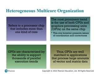
The most prominent trend in terms of heterogeneous multicore design is the use of
both CPUs and graphics processing units (GPUs)
on the same chip. Briefly, GPUs are characterized by the ability to support thousands of parallel execution
threads. Thus, GPUs are well matched to applications that process large amounts
of vector and matrix data. Initially aimed at improving the performance of graphics
applications, thanks to easy-to-adopt programming models such as CUDA
(Compute Unified Device Architecture), these new processors are increasingly
being applied to improve the performance of general-purpose and scientific
applications that involve large numbers of repetitive operations on structured data.
To deal with the diversity of target applications in today’s computing environment,
multicore containing both GPUs and CPUs has the potential to enhance performance.
This heterogeneous mix, however, presents issues of coordination and
correctness.
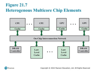
#11 Figure 21.7 is a typical multicore processor organization. Multiple CPUs and
GPUs share on-chip resources, such as the last-level cache (LLC), interconnection
network, and memory controllers. Most critical is the way in which cache management
policies provide effective sharing of the LLC.
The differences in cache sensitivity and memory access rate between CPUs and
GPUs create significant challenges to the efficient sharing of the LLC.
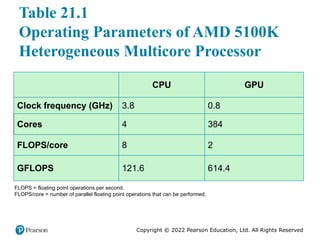
#12 Table 21.1 illustrates the potential performance benefit of combining CPUs
and GPUs for scientific applications. This table shows the basic operating parameters
of an AMD chip, the A10 5800K [ALTS12]. For floating-point calculations,
the CPU’s performance at 121.6 GFLOPS is dwarfed by the GPU, which offers 614
GFLOPS to applications that can utilize the resource effectively.
Whether it is scientific applications or traditional graphics processing, the key
to leveraging the added GPU processors is to consider the time needed to transfer a
block of data to the GPU, process it, then return the results to the main application
thread. In earlier implementations of chips that incorporated GPUs, physical memory
is partitioned between CPU and GPU. If an application thread is running on a
CPU that demands GPU processing, the CPU explicitly copies the data to the GPU
memory. The GPU completes the computation and then copies the result back to
CPU memory. Issues of cache coherence across CPU and GPU memory caches do
not arise because the memory is partitioned. On the other hand, the physical handing
of data back and forth results in a performance penalty.
#13 A number of research and development efforts are underway to improve performance
over that described in the preceding paragraph, of which the most notable
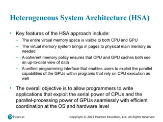
is the initiative by the Heterogeneous System Architecture (HSA) Foundation. Key
features of the HSA approach include the following:
1. The entire virtual memory space is visible to both CPU and GPU. Both CPU
and GPU can access and allocate any location in the system’s virtual memory
space.
2. The virtual memory system brings in pages to physical main memory as
needed.
A coherent memory policy ensures that CPU and GPU caches both see an
up-to-date view of data.
4. A unified programming interface that enables users to exploit the parallel
capabilities of the GPUs within programs that rely on CPU execution as well.
The overall objective is to allow programmers to write applications that
exploit the serial power of CPUs and the parallel-
processing power of GPUs seamlessly
with efficient coordination at the OS and hardware level. As mentioned, this
is an ongoing area of research and development.
#14 Another common example of a heterogeneous multicore
chip is a mixture of CPUs and digital signal processors (DSPs). A DSP provides
ultra-fast instruction sequences (shift and add; multiply and add), which are
commonly used in math-intensive digital signal processing applications. DSPs are
used to process analog data from sources such as sound, weather satellites, and
earthquake monitors. Signals are converted into digital data and analyzed using
various algorithms such as Fast Fourier Transform. DSP cores are widely used in
myriad devices, including cellphones, sound cards, fax machines, modems, hard
disks, and digital TVs.
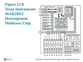
As a good representative example, Figure 21.8 shows a recent version of
Texas Instruments (TI) K2H SoC platform [TI12]. This heterogeneous multicore
processor delivers power-efficient processing solutions for high-end
imaging applications. TI lists the performance as delivering up to 352 GMACS, 198 GFLOPS,
and 19,600 MIPS. GMACS stands for giga (billions of) multiply-accumulate
operations per second, a common measure of DSP performance. Target applications for
these systems include industrial automation, video surveillance, high-end
inspection systems, industrial printers/scanners, and currency/counterfeit detection.
The TI chip includes four ARM Cortex-A15 cores and eight TI C66x DSP cores.
Each DSP core contains 32 kB of L1 data cache and 32 kB of L1 program
(instruction) cache. In addition, each DSP has 1 MB of dedicated SRAM memory
that can be configured as all L2 cache, all main memory, or a mix of the two. The
portion configured as main memory functions as a “local” main memory, referred
to simply as SRAM . This local main memory can be used for temporary data, avoiding
the need for traffic between cache and off-chip memory. The L2 cache of each of
the eight DSP cores is dedicated rather than shared with the other DSP cores. This
is typical for a multicore DSP organization: Each DSP works on a separate block of
data in parallel, so there is little need for data sharing.
Each ARM Cortex-A15 CPU core has 32-kB L1 data and program caches,
and the four cores share a 4-MB L2 cache.
The 6-MB multicore shared memory (MSM) is always configured as
all SRAM. That is, it behaves like main memory rather than cache. It can be configured
to feed directly the L1 DSP and CPU caches, or to feed the L2 DSP and CPU
caches. This configuration decision depends on the expected application profile.
The multicore shared memory controller (MSMC) manages traffic among ARM
cores, DSP, DMA, other mastering peripherals, and the external memory interface
(EMIF). MSMC controls access to the MSM, which is accessible by all the cores and
the mastering peripherals on the device.
#15 Another recent approach to heterogeneous multicore organization is the use of
multiple cores that have equivalent ISAs but vary in performance or power efficiency.
The leading example of this is ARM’s big.Little architecture, which we examine
in this section.
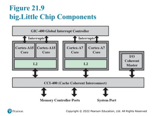
Figure 21.9 illustrates this architecture. The figure shows a multicore processor
chip containing two high-performance Cortex-A15 cores and two lower-performance,
lower-power-consuming Cortex-A7 cores. The A7 cores handle less computation-intense
tasks, such as background processing, playing music, sending
texts, and making phone calls. The A15 cores are invoked for high intensity tasks,
such as for video, gaming, and navigation.
The big.Little architecture is aimed at the smartphone and tablet market.
These are devices whose performance demands from users are increasing at a much
faster rate than the capacity of batteries or the power savings from semiconductor
process advances. The usage pattern for smartphones and tablets is quite dynamic.
Periods of processing-intense tasks, such as gaming and web browsing, alternate
with typically longer periods of low processing-intensity tasks, such as texting, e-mail,
and audio. The big.Little architecture takes advantage of this variation in
required performance. The A15 is designed for maximum performance within the
mobile power budget. The A7 processor is designed for maximum efficiency and
high enough performance to address all but the most intense periods of work.
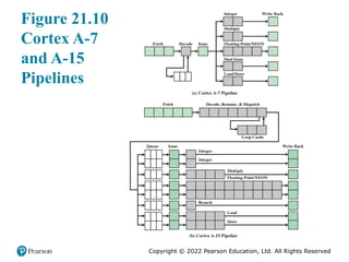
#16 The A7 is far simpler and less powerful than
the A15. But its simplicity requires far fewer transistors than does the A15’s
complexity—and fewer transistors require less energy to operate. The differences
between the A7 and A15 cores are seen most clearly by examining their instruction
pipelines, as shown in Figure 21.10.
The A7 is an in-order CPU with a pipeline length of 8 to 10 stages. It has a
single queue for all of its execution units, and two instructions can be sent to its five
execution units per clock cycle. The A15, on the other hand, is an out-of- order
processor with a pipeline length of 15 to 24 stages. Each of its eight execution units has
its own multistage queue, and three instructions can be processed per clock cycle.
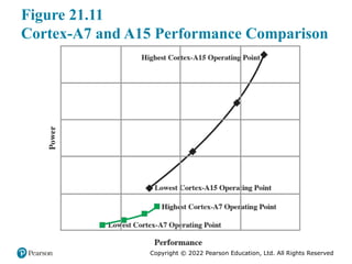
#17 The energy consumed by the execution of an instruction is partially related to
the number of pipeline stages it must traverse. Therefore, a significant difference in
energy consumption between Cortex-A15 and Cortex-A7 comes from the different
pipeline complexity. Across a range of benchmarks, the Cortex-A15
delivers roughly twice the performance of the Cortex-A7 per unit MHz, and the
Cortex-A7 is roughly three times as energy efficient as the Cortex-A15
in completing the same workloads [JEFF12]. The performance tradeoff is illustrated in
Figure 21.11 [STEV13].
#18 Typically, a heterogeneous multicore processor will feature dedicated L2 cache
assigned to the different processor types. We see that in the general depiction of a
CPU/GPU scheme of Figure 21.7. Because the CPU and GPU are engaged in quite
different tasks, it makes sense that each has its own L2 cache, shared among the similar
CPUs. We also see this in the big.Little architecture (Figure 21.9), in which the A7
cores share an L2 cache and the A15 cores share a separate L2 cache.
When multiple caches exist, there is a need for a cache-coherence scheme to
avoid access to invalid data. Cache coherency may be addressed with software-
based techniques. In the case where the cache contains stale data, the cached copy may be
invalidated and reread from memory when needed again. When memory contains
stale data due to a write-back cache containing dirty data, the cache may be cleaned
by forcing write back to memory. Any other cached copies that may exist in other
caches must be invalidated. This software burden consumes too many resources in a
SoC chip, leading to the use of hardware cache-coherent implementations, especially
in heterogeneous multicore processors.
As described in Chapter 20, there are two main approaches to hardware-implemented
cache coherence: directory protocols and snoopy protocols. ARM
has developed a hardware coherence capability called ACE (A dvanced Extensible
Interface C oherence E xtensions) that can be configured to implement either directory
or snoopy approach, or even a combination. ACE has been designed to support
a wide range of coherent masters with differing capabilities. ACE supports
coherency between dissimilar processors such as the Cortex-A15 and Cortex-A7
processors, enabling ARM big.Little technology. It supports I/O coherency for
un-cached masters, supports masters with differing cache line sizes, differing internal
cache state models, and masters with write-back or write-through caches. As
another example, ACE is implemented in the memory subsystem memory controller
(MSMC) in the TI SoC chip of Figure 21.8. MSMC supports hardware cache
coherence between the ARM CorePac L1/L2 caches and EDMA/IO peripherals for
shared SRAM and DDR spaces. This feature allows the sharing of MSMC SRAM
and DDR data spaces by these masters on the chip, without having to use explicit
software cache maintenance techniques.
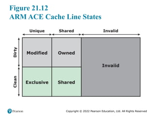
#19 ACE makes use of a five-state cache model. In each cache, each line is either
Valid or Invalid. If a line is Valid, it can be in one of four states, defined by two
dimensions. A line may contain data that are Shared or Unique. A Shared line contains
data from a region of external (main) memory that is potentially sharable. A
Unique line contains data from a region of memory that is dedicated to the core
owning this cache. And the line is either Clean or Dirty, generally meaning either
memory contains the latest, most up-to-date data and the cache line is merely a copy
of memory, or if it’s Dirty then the cache line is the latest, most up-to-date data and
it must be written back to memory at some stage. The one exception to the above
description is when multiple caches share a line and it’s dirty. In this case, all caches
must contain the latest data value at all times, but only one may be in the Shared/
Dirty state, the others being held in the Shared/Clean state. The Shared/Dirty state
is thus used to indicate which cache has responsibility for writing the data back to
memory, and Shared/Clean is more accurately described as meaning data is shared
but there is no need to write it back to memory.
The ACE states correspond to a cache coherency model with five states,
known as MOESI (Figure 21.12).
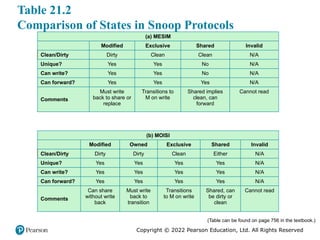
#20 Table 21.2 compares the MOESI model with the
MESI model described in Chapter 20.
#21 Intel has introduced a number of multicore products in recent years. In this section,
we look at the Intel Core i7-5960X.
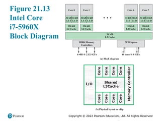
The general structure of the Intel Core i7-5960X is shown in Figure 21.13. Each
core has its own dedicated L2 cache and the eight cores share a 20-MB L3 cache . One
mechanism Intel uses to make its caches more effective is prefetching, in which the
hardware examines memory access patterns and attempts to fill the caches speculatively
with data that’s likely to be requested soon.
The Core i7-5960X chip supports two forms of external communications to
other chips. The DDR4 memory controller brings the memory controller for the
DDR main memory onto the chip. The interface supports three channels that are
8 bytes wide for a total bus width of 256 bits, for an aggregate data rate of up to
64 GB/s. With the memory controller on the chip, the Front Side Bus is eliminated.
The PCI Express is a peripheral bus. It enables high-speed communications
among connected processor chips. The PCI Express link operates at 8 GT/s
(transfers per second). At 40 bits per transfer, that adds up to 40 GB/s.
#22 We have already seen two examples of heterogeneous multicore processors using
ARM cores, in Section 21.4: the big.Little architecture, which uses a combination of
ARM Cortex-A7 and Cortex-A15 cores; and the Texas Instruments DSP SoC architecture,
which combines Cortex-A15 cores with TI DSP cores. In this section, we
introduce the Cortex-A15 MPCore multicore chip, which is a homogeneous multicore
processor using multiple A15 cores. The A15 MPCore is a high-performance
chip targeted at applications including mobile computing, high-end
digital home servers, and wireless infrastructure.
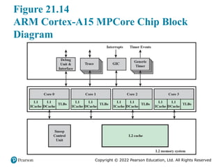
Figure 21.14 presents a block diagram of the Cortex-A15
MPCore. The key elements of the system are as follows:
■ Generic interrupt controller (GIC): Handles interrupt detection and interrupt
prioritization. The GIC distributes interrupts to individual cores.
■ Debug unit and interface: The debug unit enables an external debug host to: stop
program execution; examine and alter process and coprocessor state; examine
and alter memory and input/output peripheral state; and restart the processor.
■ Generic timer: Each core has its own private timer that can generate interrupts.
■ Trace: Supports performance monitoring and program trace tools.
■ Core: A single ARM Cortex-15 core.
■ L1 cache: Each core has its own dedicated L1 data cache and L1 instruction
cache.
■ L2 cache: The shared L2 memory system services L1 instruction and data
cache misses from each core.
■ Snoop control unit (SCU): Responsible for maintaining L1/L2 cache
coherency.
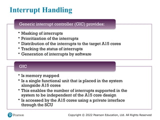
#23 The GIC collates interrupts from a large number of sources. It provides
■ Masking of interrupts
■ Prioritization of the interrupts
■ Distribution of the interrupts to the target A15 cores
■ Tracking the status of interrupts
■ Generation of interrupts by software
The GIC is a single functional unit that is placed in the system alongside A15
cores. This enables the number of interrupts supported in the system to be independent
of the A15 core design. The GIC is memory mapped; that is, control registers
for the GIC are defined relative to a main memory base address. The GIC is
accessed by the A15 cores using a private interface through the SCU.
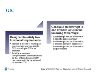
#24 The GIC is designed to satisfy two functional requirements:
■ Provide a means of routing an interrupt request to a single CPU or multiple
CPUs, as required.
■ Provide a means of interprocessor communication so that a thread on one
CPU can cause activity by a thread on another CPU.
As an example that makes use of both requirements, consider a multithreaded
application that has threads running on multiple processors. Suppose the application
allocates some virtual memory. To maintain consistency, the operating system
must update memory translation tables on all processors. The OS could update the
tables on the processor where the virtual memory allocation took place, and then
issue an interrupt to all the other processors running this application. The other
processors could then use this interrupt’s ID to determine that they need to update
their memory translation tables.
The GIC can route an interrupt to one or more CPUs in the following three
ways:
■ An interrupt can be directed to a specific processor only.
■ An interrupt can be directed to a defined group of processors. The MPCore
views the first processor to accept the interrupt, typically the least loaded, as
being best positioned to handle the interrupt.
■ An interrupt can be directed to all processors.
#25 From the point of view of software running on a particular CPU, the OS can
generate an interrupt to all but self, to self, or to specific other CPUs. For communication
between threads running on different CPUs, the interrupt mechanism is
typically combined with shared memory for message passing. Thus, when a thread is
interrupted by an interprocessor communication interrupt, it reads from the appropriate
block of shared memory to retrieve a message from the thread that triggered
the interrupt. A total of 16 interrupt IDs per CPU are available for interprocessor
communication.
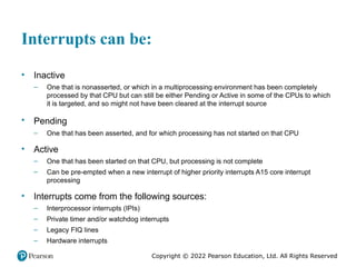
From the point of view of an A15 core, an interrupt can be:
■ Inactive: An Inactive interrupt is one that is nonasserted, or which in a multiprocessing
environment has been completely processed by that CPU but can
still be either Pending or Active in some of the CPUs to which it is targeted,
and so might not have been cleared at the interrupt source.
■ Pending: A Pending interrupt is one that has been asserted, and for which
processing has not started on that CPU.
■ Active: An Active interrupt is one that has been started on that CPU, but processing
is not complete. An Active interrupt can be pre-empted when a new
interrupt of higher priority interrupts A15 core interrupt processing.
Interrupts come from the following sources:
■ Interprocessor interrupts (IPIs): Each CPU has private interrupts, ID0-ID15,
that can only be triggered by software. The priority of an IPI depends on the
receiving CPU, not the sending CPU.
■ Private timer and/or watchdog interrupts: These use interrupt IDs 29 and 30.
■ Legacy FIQ line: In legacy IRQ mode, the legacy FIQ pin, on a per CPU basis,
bypasses the Interrupt Distributor logic and directly drives interrupt requests
into the CPU.
■ Hardware interrupts: Hardware interrupts are triggered by programmable
events on associated interrupt input lines. CPUs can support up to 224 interrupt
input lines. Hardware interrupts start at ID32.
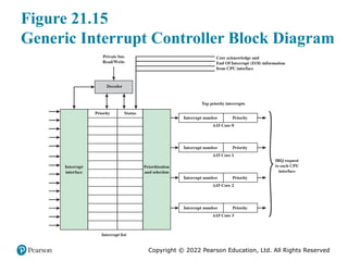
#26 Figure 21.15 is a block diagram of the GIC. The GIC is configurable to support
between 0 and 255 hardware interrupt inputs. The GIC maintains a list of interrupts,
showing their priority and status. The Interrupt Distributor transmits to each
CPU Interface the highest Pending interrupt for that interface. It receives back the
information that the interrupt has been acknowledged, and can then change the
status of the corresponding interrupt. The CPU Interface also transmits End of
Interrupt (EOI) information, which enables the Interrupt Distributor to update the
status of this interrupt from Active to Inactive.
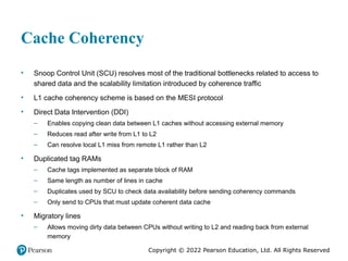
#27 The MPCore’s Snoop Control Unit (SCU) is designed to resolve most of the traditional bottlenecks related to access to shared data and the scalability limitation introduced by coherence traffic.
The L1 cache coherency scheme is based on the MESI protocol described in Chapter 20. The SCU monitors operations with shared data to optimize MESI state migration. The SCU introduces three types of optimization: direct data intervention, duplicated tag RAMs, and migratory lines.
Direct data intervention (DDI) enables copying clean data from one CPU L1 data cache to another CPU L1 data cache without accessing external memory. This reduces read after read activity from the Level 1 cache to the Level 2 cache. Thus, a local L1 cache miss is resolved in a remote L1 cache rather than from access to the shared L2 cache.
Recall that main memory location of each line within a cache is identified by a tag for that line. The tags can be implemented as a separate block of RAM of the same length as the number of lines in the cache. In the SCU, duplicated tag RAMs are duplicated versions of L1 tag RAMs used by the SCU to check for data availability before sending coherency commands to the relevant CPUs. Coherency commands are sent only to CPUs that must update their coherent data cache. This reduces the power consumption and performance impact from snooping into and manipulating each processor’s cache on each memory update. Having tag data available locally lets the SCU limit cache manipulations to processors that have cache lines in common.
The migratory lines feature enables moving dirty data from one CPU to
another without writing to L2 and reading the data back in from external memory.
The operation can be described as follows. In a typical MESI protocol, one processor
has a modified line and another processor attempts to read that line, the following
actions occur:
1. The line contents are transferred from the modified line to the processor that
initiated the read.
2. The line contents are written back to main memory.
3. The line is put in the shared state in both caches.
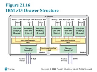
#28 The principal building block of the z13 is the processor node. Two nodes are connected
together with an inter-node S-Bus and housed in a drawer that fits into a slot
of the mainframe cabinet. A-Bus interfaces connect these two nodes with nodes in
other drawers. A z13 configuration can have up to four drawers.
The key components of a node are shown in Figure 21.16:
■ Processor unit (PU): There are three PU chips, each containing eight 5-GHz
processor cores plus three levels of cache. The PUs have external connections
to main memory via memory control units and to I/O via host channel adapters.
Thus, each node includes 24 cores.
■ Storage control (SC): The two SC chips contain an additional level of cache
(L4) plus interconnection logic for connecting to other nodes.
■ DRAM memory slots: providing up to 1.28 GB of main memory.
■ PCie slots: Slots for connection to PCIe I/O drawers.
■ GX++: Slots for connection to InfiniBand.
■ S-Bus: Connection to other nodes in this drawer.
■ A-Bus: Connection to other drawers.
■ Processor support interface (PSI): connects to system control logic.
The microprocessor core features a wide superscalar, out-of-order pipeline
that can decode six z/Architecture CISC instructions per clock cycle (< 0.18 ns)
and execute up to ten operations per cycle. Execution can occur out of program order.
The instruction execution path is predicted by branch direction and target prediction logic.
Each core includes four integer units, two load/store units, two binary floating-point units, and two vector
floating-point units.
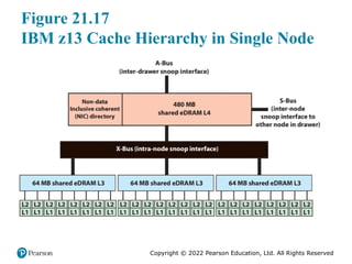
#29 The zEC12 incorporates a four level cache structure. We look at each level in turn
(Figure 21.17).
Each core has a dedicated 96-kB L1 I-cache and a 128-kB L1 D-cache. The L1
cache is designed as a write-through cache to L2, that is, altered data are also stored
to the next level of memory. These caches are eight-way set associative.
Each core also has a dedicated 2-MB L2, split equally into 1-MB data cache
and 1-MB instruction cache. The L2 caches are write-through to L3, and eight-way
set associative.
Each eight-core processor unit chip includes a 64-MB L3 cache shared by all
eight cores. Because L1 and L2 caches are write-through, the L3 cache must process
every store generated by the eight cores on its chip. This feature maintains data
availability during a core failure. The L3 cache is 16-way set associative. The z13
implements embedded DRAM (eDRAM) as L3 cache memory on the chip. While
this eDRAM memory is slower than static RAM (SRAM) traditionally used to
implement cache memory, the eDRAM can hold significantly more bits in a given
surface area. For many workloads, having more memory closer to the core is more
important than having fast memory.
The three PUs in a node share a 480-MB L4 cache. The L4 cache is on a
chip that also includes a non-data inclusive coherent (NIC) directory that points
to L3-owned lines that have not been included in L4 cache. The principal motivation
for incorporating a level 4 cache is that the very high clock speed of the core
processors results in a significant mismatch with main memory speed. The fourth
cache layer is needed to keep the cores running efficiently. The large shared L3 and
L4 caches are suited to transaction-processing workloads exhibiting a high degree
of data sharing and task swapping. The L4 cache is 30-way set associative. The SC
chip, which houses the L4 cache, also acts as a cross-point switch for L4-to-L4 traffic
to up to the other node in the same drawer and two other drawers by bidirectional
data buses. The L4 cache is the coherence manager, meaning that all memory
fetches must be in the L4 cache before that data can be used by the processor.
All four caches use a line size of 256 bytes.
The z13 is an interesting study in design trade-offs and the difficulty in exploiting
the increasingly powerful processors available with current technology. The large L4
cache is intended to drive the need for access to main memory down to the bare minimum.
However, the distance to the off-chip L4 cache costs a number of instruction
cycles. Thus, the on-chip area devoted to cache is as large as possible, even to the point
of having fewer cores than possible on the chip. The L1 caches are small, to minimize
distance from the core and ensure that access can occur in one cycle. Each L2 cache is
dedicated to a single core, in an attempt to maximize the amount of cached data that
can be accessed without resorting to a shared cache. The L3 cache is shared by all four
cores on a chip and is as large as possible, to minimize the need to go to the L4 cache.
Because all of the nodes of the z13 share the workload, all of the L4 caches
form a single L4 cache memory. Thus, access to L4 means not only going off-chip
but perhaps off-drawer, further increasing access delay. This means relatively large
distances exist between the higher-level caches in the processors and the L4 cache
content. Still, accessing L4 cache data on another node is faster than accessing
DRAM on the other node, which is why the L4 caches work this way.
To overcome the delays that are inherent to this design and to save cycles
to access the off-node L4 content, the designers try to keep instructions and data
as close to the cores as possible by directing as much work as possible of a given
logical partition workload to the cores located in the same node as the L4 cache.
This is achieved by having the system and the z/OS dispatcher work together to
keep as much work as possible within the boundaries of as few cores and L4 cache
space (which is best within a node boundary) as can be achieved without affecting
throughput and response times. Preventing the resource manager/scheduler and
the dispatcher from assigning workloads to processors where they might run less
efficiently, contributes to overcoming latency in a high-frequency processor design
such as the z13.