In this chapter,we will derive
the conductive current of a
diode.
3.
• Suppose weare given a PN junction as shown in the following figure.
• In the region labelled as p-type, the density of the majority carriers is . Hence,
the density of the minority carriers .
• Similarly, in the region labelled as n-type, the density of the majority carriers is .
Hence, the density of the minority carriers .
• In the absence of any bias, all the carrier concentrations should remain constant
until they reach the contact interface between P-type region and N-type region.
• However, under a forward bias, the concentration of a minority carrier changes
as a result of the mechanism known as low-level injection.
4.
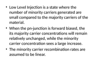
• Low LevelInjection is a state where the
number of minority carriers generated are
small compared to the majority carriers of the
material.
• When the pn-junction is forward biased, the
its majority carrier concentrations will remain
relatively unchanged, while the minority
carrier concentration sees a large increase.
• The minority carrier recombination rates are
assumed to be linear.
5.
What happen ifthe diode is
forward biased by an external
supply voltage?
6.
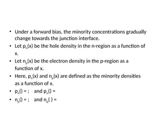
• Under aforward bias, the minority concentrations gradually
change towards the junction interface.
• Let pn(x) be the hole density in the n-region as a function of
x.
• Let np(x) be the electron density in the p-region as a
function of x.
• Here, pn(x) and np(x) are defined as the minority densities
as a function of x.
• pn() = ; and pn() =
• np() = ; and np( ) =
Further Explanation ofthis Low Level Injection
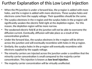
• When the PN junction is under a forward bias, the p-region is added with more
holes, and the n-region is added with more electrons. These surplus holes and
electrons come from the supply voltage. Their quantities should be the same.
• The surplus electrons in the n-region and the surplus holes in the p-region will
significantly weaken the electric field right at the depletion region. For this
reason, the depletion region will be more narrow.
• The weakened electric field E at the junction will not be able to overcome the
diffusion current. Eventually, diffusion will take place as a result of the
concentration gradient.
• Under the forward bias, the surplus electrons in the n-region will be driven
across the junction and will eventually recombine with holes in the p-region.
• Similarly, the surplus holes in the p-region will eventually recombine with
electrons supplied by the supply voltage.
• The minority carriers are injected across the junction under a condition that the
minority carrier concentration is small compared to the majority carrier
concentration. This injection is known as low level injection.
• The majority carrier concentration will be virtually unaffected.
9.
• As aresult of the recombination process, the
minority carrier concentration gradually decreases
against x.
• The concentration profiles for the minority carriers
are a function of x (Please see Fig. 1): i.e. pn(x) and
np(x), which are not derived in this course.
• Instead of using + or -, we replace these quantities
with and . Lp and Ln are respectively defined as the
diffusion lengths for holes and electrons.
• pn(x) and np(x) are given here without any proof as:
=+ (1)
np= + (2)
10.
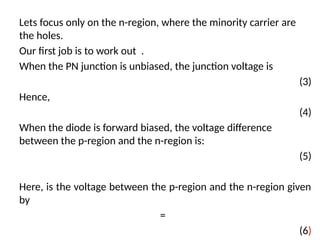
Lets focus onlyon the n-region, where the minority carrier are
the holes.
Our first job is to work out .
When the PN junction is unbiased, the junction voltage is
(3)
Hence,
(4)
When the diode is forward biased, the voltage difference
between the p-region and the n-region is:
(5)
Here, is the voltage between the p-region and the n-region given
by
=
(6)
11.
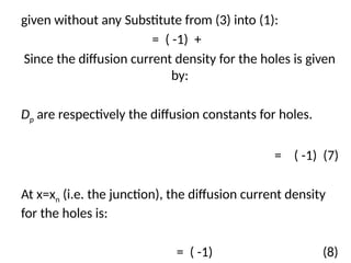
given without anySubstitute from (3) into (1):
= ( -1) +
Since the diffusion current density for the holes is given
by:
Dp are respectively the diffusion constants for holes.
= ( -1) (7)
At x=xn (i.e. the junction), the diffusion current density
for the holes is:
= ( -1) (8)
12.
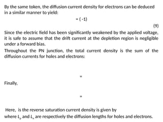
By the sametoken, the diffusion current density for electrons can be deduced
in a similar manner to yield:
= ( -1)
(9)
Since the electric field has been significantly weakened by the applied voltage,
it is safe to assume that the drift current at the depletion region is negligible
under a forward bias.
Throughout the PN junction, the total current density is the sum of the
diffusion currents for holes and electrons:
=
Finally,
=
Here, is the reverse saturation current density is given by
where Lp and Ln are respectively the diffusion lengths for holes and electrons.
13.
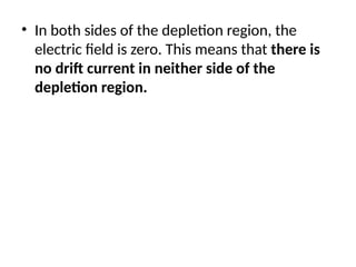
• In bothsides of the depletion region, the
electric field is zero. This means that there is
no drift current in neither side of the
depletion region.
14.
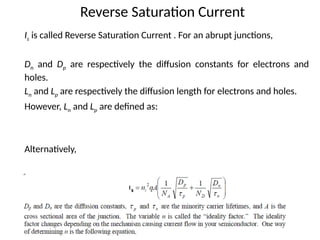
Reverse Saturation Current
Isis called Reverse Saturation Current . For an abrupt junctions,
Dn and Dp are respectively the diffusion constants for electrons and
holes.
Ln and Lp are respectively the diffusion length for electrons and holes.
However, Ln and Lp are defined as:
Alternatively,
15.
Diffusion Capacitance
Differentiate itwith respect to V:
=
=
Conclusion:
The small signal diffusion capacitance of a PN junction is
proportional to the forward current. The larger voltage
you apply, the larger the capacitance is.
16.
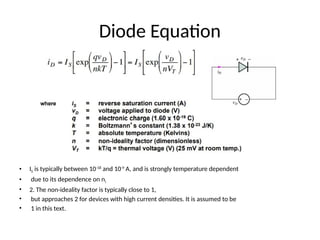
Diode Equation
• ISis typically between 10-18
and 10-9
A, and is strongly temperature dependent
• due to its dependence on ni
• 2. The non-ideality factor is typically close to 1,
• but approaches 2 for devices with high current densities. It is assumed to be
• 1 in this text.
17.
Diode Characteristics
• Turnon voltage marks the transition from low current to high current.
• Is is the reverse saturation current
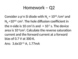
Homework – Q2
Considera p+
n Si diode with Na = 1018
/cm3
and
Nd =1016/
cm3
. The hole diffusion coefficient in
the n-side is 10 cm2
/s and = 10-7
s. The device
area is 10-4
cm2
. Calculate the reverse saturation
current and the forward current at a forward
bias of 0.7 V at 300 K.
Ans: 3.6x10⁻¹⁵
A, 1.77mA


![Current Density in forward bias[2][1].pptx](https://cdn.slidesharecdn.com/ss_thumbnails/currentdensityinforwardbias21-251218104548-e92f2beb-thumbnail.jpg?width=640&height=640&fit=bounds)


