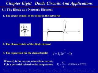
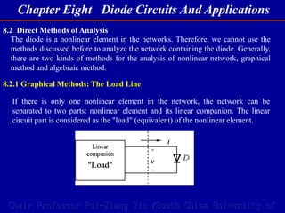
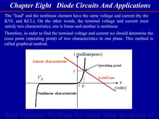
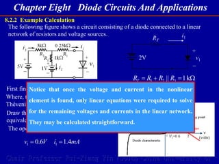
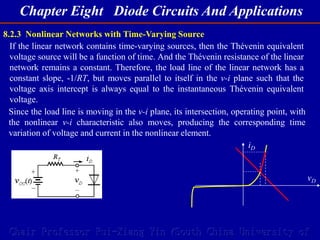
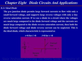
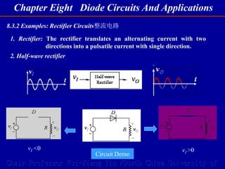
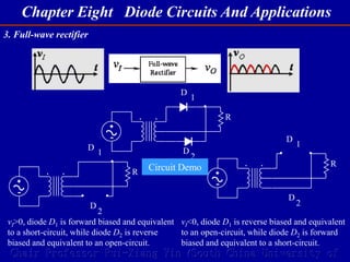
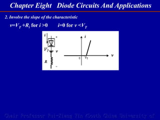
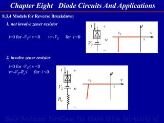
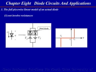
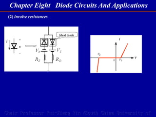
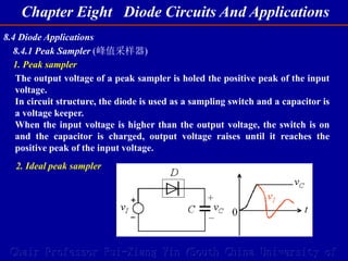
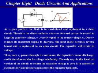
1. Chair Professor Rui-Xiang Yin (South China University of
Chapter Eight Diode Circuits And Applications
8.1 The Diode as a Network Element
8.2 Direct Methods of Analysis
8.3 Piecewise linear Models of Diode Behavior
8.4 Diode Applications
Contents of this Chapter:
2. Chapter Eight Diode Circuits And Applications
Chair Professor Rui-Xiang Yin (South China University of
8.1 The Diode as a Network Element
1. The circuit symbol of the diode in the networks
2. The characteristic of the diode element
3. The expression for the characteristic
Where IS is the reverse saturation current,
VT is a potential related to the temperature
( 1)
T
v
V
S
i I e
, (25.8mV at 27 C)
T
kT
V
q
3. Chapter Eight Diode Circuits And Applications
Chair Professor Rui-Xiang Yin (South China University of
8.2 Direct Methods of Analysis
The diode is a nonlinear element in the networks. Therefore, we cannot use the
methods discussed before to analyze the network containing the diode. Generally,
there are two kinds of methods for the analysis of nonlinear network, graphical
method and algebraic method.
8.2.1 Graphical Methods: The Load Line
If there is only one nonlinear element in the network, the network can be
separated to two parts: nonlinear element and its linear companion. The linear
circuit part is considered as the "load" (equivalent) of the nonlinear element.
4. Chapter Eight Diode Circuits And Applications
Chair Professor Rui-Xiang Yin (South China University of
The "load" and the nonlinear element have the same voltage and current (by the
KVL and KCL). On the other words, the terminal voltage and current must
satisfy two characteristics, one is linear and another is nonlinear.
Therefore, in order to find the terminal voltage and current we should determine the
cross point (operating point) of two characteristics in one plane. This method is
called graphical method.
5. Chapter Eight Diode Circuits And Applications
Chair Professor Rui-Xiang Yin (South China University of
8.2.2 Example Calculation
The following figure shows a circuit consisting of a diode connected to a linear
network of resistors and voltage sources.
First find the Thévenin equivalent for the linear network.
2V
RT
+
_
v1
i1
Where, the open-circuit voltage can be determined by superposition, and the
Thévenin resistance is 1 kohm.
1 2 3
|| 1k
T
R R R R
Draw the v-i characteristic of this
equivalent and the diode in one plane.
The operating point is found in the figure that
1 1
0.6 1.4
v V i mA
Notice that once the voltage and current in the nonlinear
element is found, only linear equations were required to solve
for the remaining voltages and currents in the linear network.
They may be calculated straightforward.
6. Chapter Eight Diode Circuits And Applications
Chair Professor Rui-Xiang Yin (South China University of
8.2.3 Nonlinear Networks with Time-Varying Source
If the linear network contains time-varying sources, then the Thévenin equivalent
voltage source will be a function of time. And the Thévenin resistance of the linear
network remains a constant. Therefore, the load line of the linear network has a
constant slope, -1/RT, but moves parallel to itself in the v-i plane such that the
voltage axis intercept is always equal to the instantaneous Thévenin equivalent
voltage.
Since the load line is moving in the v-i plane, its intersection, operating point, with
the nonlinear v-i characteristic also moves, producing the corresponding time
variation of voltage and current in the nonlinear element.
vD
iD
7. Chapter Eight Diode Circuits And Applications
Chair Professor Rui-Xiang Yin (South China University of
8.2.4 Networks with More than One Nonlinear Element*
If a circuit contains more than one nonlinear element, graphical solutions,
while possible, become more complex. First, it is not possible to separate
the circuit into a linear part and a single nonlinear element. Thus the
network facing a given nonlinear element contains at least one nonlinear
element, and the v-i characteristic at its terminals will produce a nonlinear
load line. Of course, the intersection of the nonlinear load line with the
remaining nonlinear characteristic produces the desired operating point;
the difficulty is with the construction of the nonlinear load line. If the
network contains only two nonlinear elements, a graphical solution can be
obtained with only a modest increase in complexity. For cases with more
than two nonlinear elements, the effort required for graphical solutions is
seldom justified. For this reason we seek alternate methods of solution to
networks with nonlinear elements, some of which we will now describe.
8. Chapter Eight Diode Circuits And Applications
Chair Professor Rui-Xiang Yin (South China University of
8.2.5 Algebraic Methods: The Exponential and Logarithmic Amplifier
Because the diode has an exponential characteristic, it is possible to construct
the exponential or logarithmic amplifier using the diode and op-amps.
If the element A has characteristic i =f1(vi)
Then the output voltage would be vo=f2(f1(vi))
According to the selection of components A and F, two special amplifiers can be
constructed.
and the element F has characteristic vo=f2(i).
9. Chapter Eight Diode Circuits And Applications
Chair Professor Rui-Xiang Yin (South China University of
1. Exponential amplifier
Let element A be a diode ( 1)
T
v
V
S
i I e
element F a resistor R 0
v R i
The transfer characteristic of the circuit is
0 for 10
i
q
v
kT
S i
kT
v R I e v
q
Circuit Demo
10. Chapter Eight Diode Circuits And Applications
Chair Professor Rui-Xiang Yin (South China University of
2. Logarithmic amplifier
Let element A be a resistance R:
element F a diode D
The transfer characteristic of the circuit is
0
( 1)
T
v
V
S
i I e
i
v
i
R
0 ln for
i
i S
S
v
q
v v RI
kT R I
Circuit Demo
11. Chapter Eight Diode Circuits And Applications
Chair Professor Rui-Xiang Yin (South China University of
8.3 Piecewise linear Models of Diode Behavior
In networks with several nonlinear elements, the graphical and algebraic
methods become very complex. Furthermore, in a network containing an
energy storage element, the graphical technique cannot handle adequately
the dynamic responses to time-varying inputs.
An alternate and very useful approach is to represent the nonlinear v-i
characteristic in pieces with a set of approximate but linear v-i
characteristics, each one valid over a suitably restricted range of voltage
and current. In fact, we have already used this approach in discussing op-
amps. The complete op-amp transfer characteristic was represented in
three linear segments: a linear gain region and two saturation regions. As
long as we were careful to check that the voltages and currents in the
proper ranges, it was possible to represent the nonlinear op-amp with a
piecewise linear model.
12. Chapter Eight Diode Circuits And Applications
Chair Professor Rui-Xiang Yin (South China University of
8.3.1 Ideal Diode
The p-n junction diode permits large forward currents to flow with only a
small forward voltage, and supports large reverse voltages with only a tiny
reverse saturation current. If we use a diode in a circuit where the voltages
are much large compared to the diode forward voltage and the currents are
much large compared to the diode reverse saturation current, then both the
diode forward voltage and diode reverse current can be neglected. This is
the ideal diode, which characteristic is represented as
v=0 for i >0 i=0 for v <0
13. Chapter Eight Diode Circuits And Applications
Chair Professor Rui-Xiang Yin (South China University of
8.3.2 Examples: Rectifier Circuits整流电路
1. Rectifier: The rectifier translates an alternating current with two
directions into a pulsatile current with single direction.
2. Half-wave rectifier
vI >0
vI <0
Circuit Demo
14. Chapter Eight Diode Circuits And Applications
Chair Professor Rui-Xiang Yin (South China University of
3. Full-wave rectifier
D
D
2
1
R
D
D
2
1
R
D
D
2
1
R
vI>0, diode D1 is forward biased and equivalent
to a short-circuit, while diode D2 is reverse
biased and equivalent to an open-circuit.
vI<0, diode D1 is reverse biased and equivalent
to an open-circuit, while diode D2 is forward
biased and equivalent to a short-circuit.
Circuit Demo
15. Chapter Eight Diode Circuits And Applications
Chair Professor Rui-Xiang Yin (South China University of
8.3.3 Improved Models for Forward Bias
In many circuits, the source voltages present are not large compared to the
threshold voltage (0.6V in silicon or 0.3V in germanium). In such circuits, the
representation of a forward biased diode as a perfect short circuit is too drastic
a simplification. In this case, we should use more accurate model (combine an
ideal diode and other additional elements) to represent the diode.
1. Involve the threshold voltage
v=VT for i >0 i=0 for v <VT
16. Chapter Eight Diode Circuits And Applications
Chair Professor Rui-Xiang Yin (South China University of
2. Involve the slope of the characteristic
v=VT +Ri for i >0 i=0 for v <VT
17. Chapter Eight Diode Circuits And Applications
Chair Professor Rui-Xiang Yin (South China University of
8.3.4 Models for Reverse Breakdown
1. not involve zener resistor
i=0 for -VZ< v <0 v=-VZ for i <0
2. involve zener resistor
i=0 for -VZ< v <0
v=-VZ-Rz·i for i <0
18. Chapter Eight Diode Circuits And Applications
Chair Professor Rui-Xiang Yin (South China University of
3. The full piecewise linear model of an actual diode
(1) not involve resistances
19. Chapter Eight Diode Circuits And Applications
Chair Professor Rui-Xiang Yin (South China University of
(2) involve resistances
20. Chapter Eight Diode Circuits And Applications
Chair Professor Rui-Xiang Yin (South China University of
8.4 Diode Applications
8.4.1 Peak Sampler (峰值采样器)
1. Peak sampler
The output voltage of a peak sampler is holed the positive peak of the input
voltage.
In circuit structure, the diode is used as a sampling switch and a capacitor is
a voltage keeper.
When the input voltage is higher than the output voltage, the switch is on
and the capacitor is charged, output voltage raises until it reaches the
positive peak of the input voltage.
2. Ideal peak sampler
21. Chapter Eight Diode Circuits And Applications
Chair Professor Rui-Xiang Yin (South China University of
As vI goes positive, the diode is forward-biased and equivalent to a short
circuit. Therefore the diode conducts whatever forward current is needed to
keep the capacitor voltage, vC, exactly equal to the source voltage, vI. Once vI
reaches its maximum begins to decrease, the ideal diode becomes reverse
biased and is equivalent to an open circuit. The capacitor will retain its
voltage.
Thus, once vI passes through its maximum, the capacitor cannot discharge,
and it therefore retains its voltage indefinitely. The only way, in this idealized
version of the circuit, to return the capacitor voltage to zero is to connect an
external short circuit once again across the capacitor terminals.
22. Chapter Eight Diode Circuits And Applications
Chair Professor Rui-Xiang Yin (South China University of
3. The effect of forward diode drop and load resistor on peak sampler
In practice, there are several ways in which actual peak samplers depart in
their behavior from the ideal. First, with an actual diode replacing the ideal
diode, the capacitor charges to a voltage that is smaller than the peak of vI
by an amount equal to the forward voltage drop on the diode, roughly 0.6 V
for silicon. Second, a resistor has been added to represent either an external
circuit (such as a voltmeter) or the leakage resistance of the capacitor.
In either case, the finite resistance shunting the capacitor allows the
capacitor to discharge with time constant RC even after the diode becomes
reverse-biased. Thus the peak voltage on the capacitor is less than the actual
waveform peak, and it decays at a rate dependent on the current paths for
discharge. (The reverse saturation current of the diode also provides a
discharge path for the capacitor.)
Peak samplers in which the above
errors are largely eliminated can be
constructed using op-amps and
feedback.
23. Chapter Eight Diode Circuits And Applications
Chair Professor Rui-Xiang Yin (South China University of
8.4.2 A Power Supply Rectifier电源整流电路
The rectifiers are already shown in 8.3.2. In this section we discuss the
power supply rectifier with a capacitance load and sin-wave input voltage.
1. Full-Wave rectifier without the capacitor
When the secondary voltage of the
transformer, v1, is positive (>0), the
diode D1 is forward-bias and D2 is
reverse-bias. Then a current flows
through D1 and RL.
While the secondary voltage of the
transformer, v1, is negative (<0), the
diode D2 is forward-bias and D1 is
reverse-bias. A current flows through
D2 and RL.
In either cases, the current through
the load, RL, is from top to bottom in
the circuit. Therefore, the voltage on
the load resistance should be always
positive ( single polarity but identity).
24. Chapter Eight Diode Circuits And Applications
Chair Professor Rui-Xiang Yin (South China University of
The average output voltage, DC voltage, is
Where, V1 is the virtual value (r-m-s) of secondary voltage, v1, of the transformer.
0 1 1
2
0.9
m
V V V
25. Chapter Eight Diode Circuits And Applications
Chair Professor Rui-Xiang Yin (South China University of
2. Full-Wave rectifier with the capacitor
When v1 exceeds the capacitor voltage vo. diode D1 will conduct, charging up the capacitor.
When -vo < v1 < vo, diodes D1 and D2 will cut-off, discharging the capacitor through the resistance RL
When v1 < -vo, diode D2 will conduct, charging up the capacitor again.
26. Chapter Eight Diode Circuits And Applications
Chair Professor Rui-Xiang Yin (South China University of
The operating waveform of the Full-Wave rectifier with the capacitor is shown as
follows
The average output voltage,
DC voltage, is determined by
the time constant of capacitor
and
1 0 1
0.9 2
V V V
Where, V1 is the virtual value (r-m-s) of secondary voltage, v1, of the transformer.
In engineering, if the RLC>10it may be calculated approximately
0 1
1.2
V V
27. Chapter Eight Diode Circuits And Applications
Chair Professor Rui-Xiang Yin (South China University of
8.4.3 Diode Clamps and Limiters 二极管钳位和限幅电路
1. Ideal diode limiter
Since diode become strongly conducting when the forward voltage exceeds
the threshold, diodes can be used to limit or clamp the excursion of voltages
in a network. In the circuit bellow the diode will conduct a forward current
whenever the input voltage vI exceeds the battery voltage V.
When vI >V, the diode is forward bias and equivalent to a short-circuit. Then,
When vI <V, the diode is reverse bias and equivalent to a open-circuit. Then,
0 I
v V for v V
0 I I
v v for v V
28. Chapter Eight Diode Circuits And Applications
Chair Professor Rui-Xiang Yin (South China University of
2. Bipolar limiter
By reversing the diode, the limiter can be made to prevent the output voltage
from ever becoming less than the battery voltage. Also, by reversing the
polarity of the battery, limiting can be made to occur for negative values of
output voltage. This circuit and its variations are used as protection circuits
to prevent burnout of semiconductor devices through excessive voltage, and
to produce waveforms of constant amplitude for FM and digital signal
applications.
Positive limiter Negative limiter
Bipolar limiter
29. Chapter Eight Diode Circuits And Applications
Chair Professor Rui-Xiang Yin (South China University of
3. Diode protection circuit
A dc source is connected to a relay coil (modeled as an inductor). When the
switch is opened, the current in the inductor must drop rapidly to zero,
producing a strongly negative transient in vL. If an alternate path is not
provided for this current, the transient will get big enough to produce a spark
across the switch (this principle is used to ignite the spark plug in an
automobile engine).
The diode provides an alternate path for
the current, limiting the negative
excursion of vL to the threshold voltage
of the diode. Sparks across the switch are
prevented, and the current in the
inductor decays smoothly, dissipating the
inductive stored energy in diode. Often, a
small resistor is put in series with the
diode. This diode is often called "free-
wheeling" diode. 泄放二极管
30. Chapter Eight Diode Circuits And Applications
Chair Professor Rui-Xiang Yin (South China University of
8.4.4 A DC Power Supply Employing a Zener Diode Regulator
稳压二极管稳压直流电源
1. The purpose of regulating? The output of a power rectifier with capacitor
In practice, the load of a DC power may be
uncertain usually. The ripple is varied with
the load current, or load resistance. On the
other hand, the output DC voltage will be
changed by AC voltage and the load current.
This uncertain output DC voltage is not
expected in applications. Therefore, the
output of a power rectifier should be
regulated in order to obtain a unchanged DC
voltage.
2. How to regulate?
As we know, the terminal voltage of a reverse breakdown zener diode is fixed.
If a zener diode is connected in parallel across the output terminals, as long as
the diode is reverse breakdown the output must be fixed to the breakdown
voltage of the diode in spite of changing of input voltage and load.
31. Chapter Eight Diode Circuits And Applications
Chair Professor Rui-Xiang Yin (South China University of
The changeable components (ripple
and instability) of the rectifier are
absorbed by resistance R. R also
protects the excess current through
the zener diode, so it is called
current- limit resistance. Here is the
operating waveforms
32. Chapter Eight Diode Circuits And Applications
Chair Professor Rui-Xiang Yin (South China University of
3. Determination of current-limit resistance
In the circuit, there are two worst cases:
(1) The input voltage is maximum and the load current is minimum. In this
case, the zener diode carries maximum current, which should less than the
maximum allowable current of the diode:
max
min max
C Z
Z L Z
V V
I I I
R
(2) The input voltage is minimum and the load current is maximum. In this
case, the zener diode carries minimum current, which should greater than the
minimum stabilized current of the diode:
min
max min
C Z
Z L Z
V V
I I I
R
where, VC is the average (DC component) of the capacitor voltage, which can be
calculated by 1.2V1. Therefore, the allowable range of the current-limit
resistance R can be determined as
max min
min max max min
C Z C Z
L Z L Z
V V V V
R
I I I I
33. Chapter Eight Diode Circuits And Applications
Chair Professor Rui-Xiang Yin (South China University of
The Exercises of Chapter 8:
E8.2, E8.3, E8.4, E8.5, E8.8, E8.9*, E8.10, E8.11