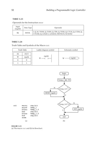
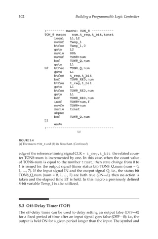
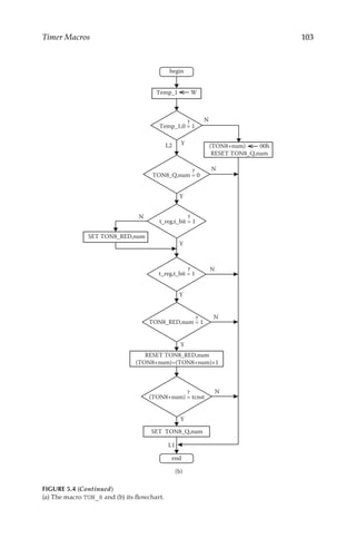
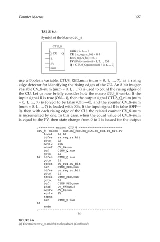
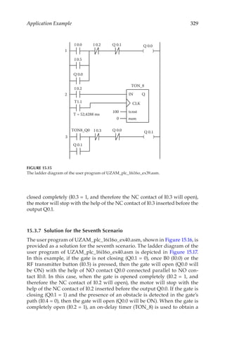
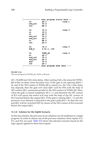
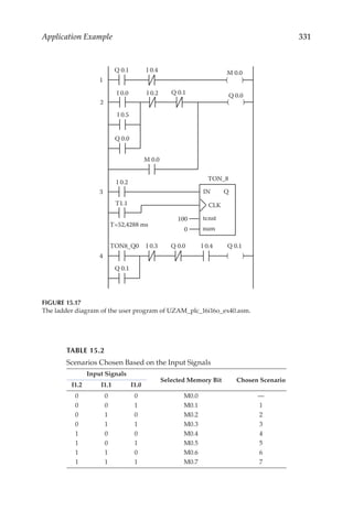
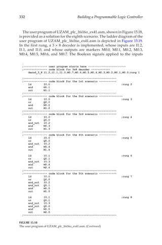
Download to read offline


![xvii
Background and Use of the Book
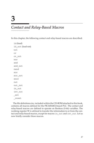
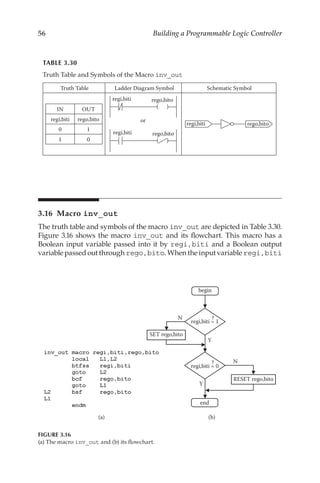
This project was completed during the search for an answer to the follow-
ing question: How could one design and implement a programmable logic
controller (PLC)? The answer to this question was partially discovered about
15 years ago by the author in a freely available PLC project called PICBIT.
The file, called picbit.inc of PICBIT, contains the basic PLC macro definitions.
The PIC16F648A-based PLC project has been completed by the inspiration of
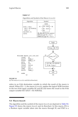
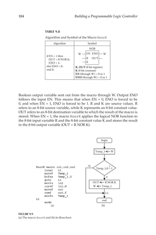
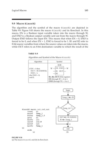
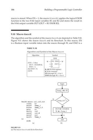
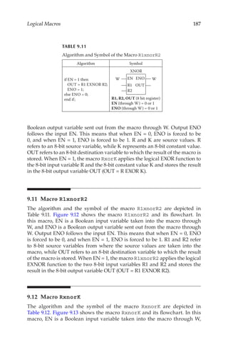
these macros. Of course many new features have been included within the
PIC16F648A-based PLC project to make it an almost perfect PLC. The reader
should be aware that this project does not include graphical interface PC
software as in PICBIT or in other PLCs for developing PLC programs. Rather,
PLC programs are developed by using macros as done in the Instruction
List (IL) PLC programming language. An interested and skilled reader could
well (and is encouraged to) develop graphical interface PC software for easy
use of the PIC16F648A-based PLC.
The PIC16F648A-based PLC project was first reported in a series of 22 arti-
cles published in Electronics World magazine (http:/
/www.electronicsworld.
co.uk/) between the years 2008 and 2010 [1–22]. All details of this project
can be viewed at http/
/www.meliksah.edu.tr/muzam/UZAM_PLC_with_
PIC16F648A.htm [23]. This book is based on an improved version of the
project reported in Electronics World magazine. The improvements are sum-
marized as follows:
1. The current hardware has two boards: the CPU board and the I/O
extension board. In the previous version of the hardware, the main
board consisted of the CPU board and eight inputs/eight outputs,
while in the current version, the CPU board excludes eight inputs/
eight outputs. Thus, the CPU board is smaller than the previous
main board. In addition, the current I/O extension board is also
smaller than in the previous version.
2. The hardware explained in this book consists of one CPU board and
two I/O extension boards. Therefore, the current version of the soft-
ware supports 16 inputs and 16 outputs, while the previous one sup-
ported 8 inputs and 8 outputs.
3. Clock frequency was 4 MHz in the previous version, but is 20 MHz
in the current version.
4. Someofthemacrosareimprovedcomparedwiththepreviousversions.
5. Flowcharts are provided to help the understanding of all macros
(functions).](https://image.slidesharecdn.com/buildingaprogrammablelogiccontrollerwithapic16f648amicrocontrollerlenguajeasembler-220618154203-89548f6a/85/Building-a-Programmable-Logic-Controller-with-a-PIC16F648A-Microcontroller-lenguaje-asembler-pdf-18-320.jpg)
![xviii Background and Use of the Book
In order to properly follow the topics explained in this book, it is expected
that the reader will construct his or her PIC16F648A-based PLC consist-
ing of the CPU board and two I/O extension boards using the PCB files
provided within the CD-ROM attached to this book. In this book, as the
PIC assembly is used as the programming language within the MPLAB
integrated development environment (IDE), the reader is referred to the
homepage of Microchip (http://www.microchip.com/) to obtain the latest
version of MPLAB IDE. References [24] and [25] may be useful to under-
stand some aspects of the PIC16F648A microcontroller and MPASM™
assembler, respectively.
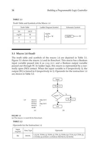
The contents of the book’s 15 chapters are explained briefly, as follows:
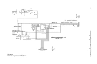
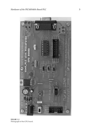
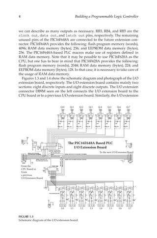
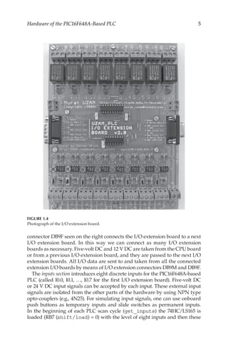
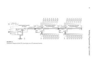
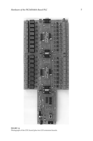
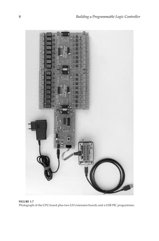
1. Hardware: Inthischapter,thehardwarestructureofthePIC16F648A-
based PLC, consisting of 16 discrete inputs and 16 discrete outputs,
is explained in detail.
2. Basic software: This chapter explains the basic software structure
of the PIC16F648A-based PLC. A PLC scan cycle includes the fol-
lowing: obtain the inputs, run the user program, and update the
outputs. In addition, it is also necessary to define and initialize all
variables used within a PLC. Necessary functions are all described
as PIC assembly macros to be used in the PIC16F648A-based PLC.
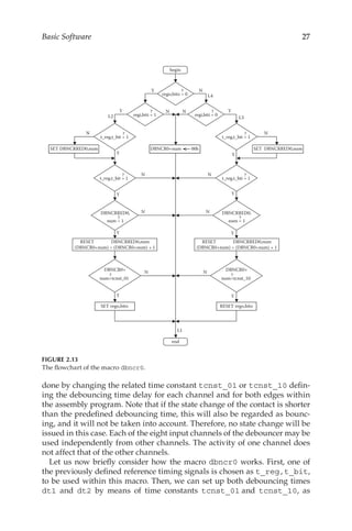
The macros described in this chapter can be summarized as follows:
HC165 (for handling the inputs), HC595 (for sending the outputs),
dbncr0 and dbncr1 (for debouncing 16 inputs), initialize,
get_inputs, and send_outputs.
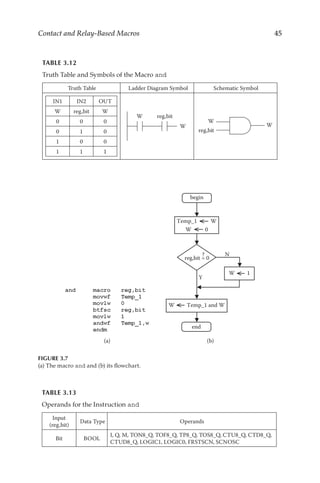
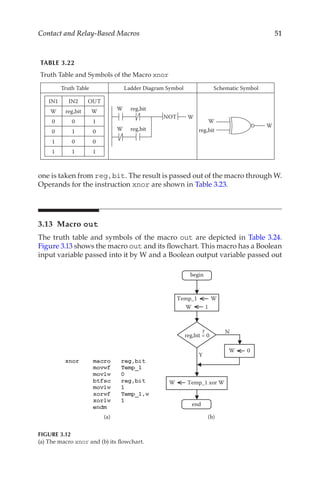
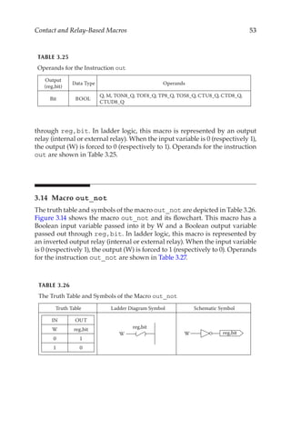
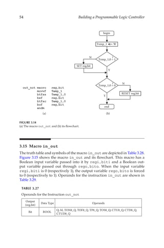
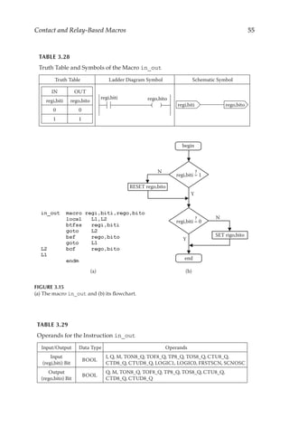
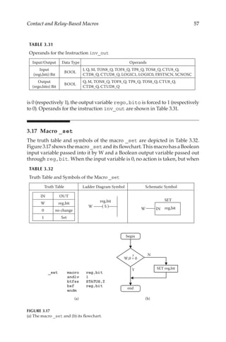
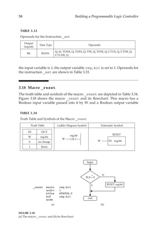
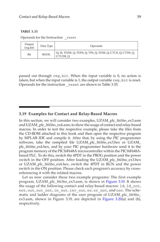
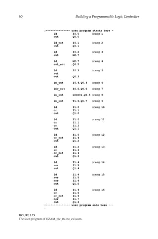
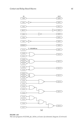
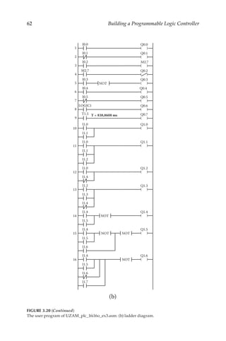
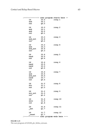
3. Contact and relay-based macros: The following contact and relay-
based macros are described in this chapter: ld (load), ld_not (load_
not), not, or, or_not, nor, and, and_not, nand, xor, xor_not,
xnor, out, out_not, in_out, inv_out, _set, _reset. These
macros are defined to operate on 1-bit (Boolean) variables.
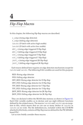
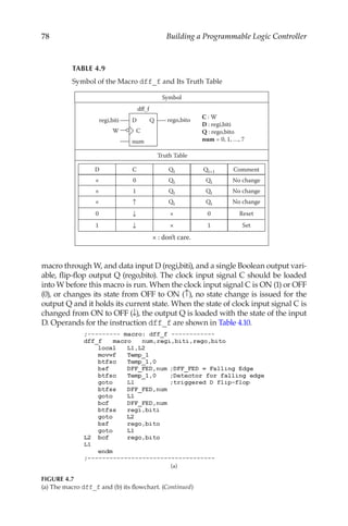
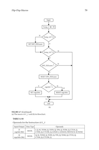
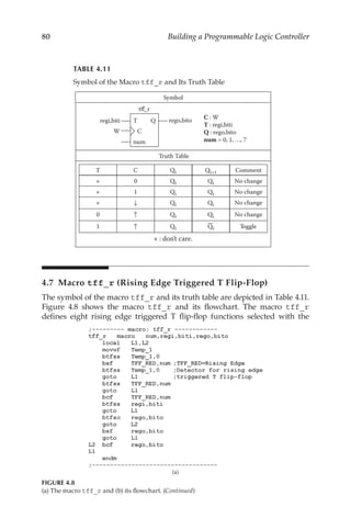
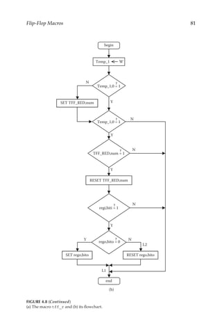
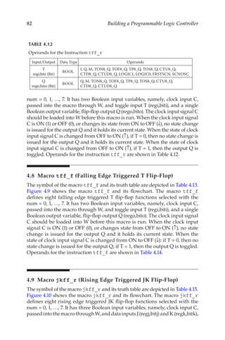
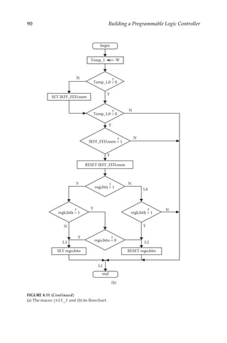
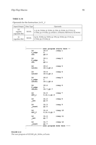
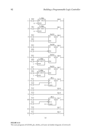
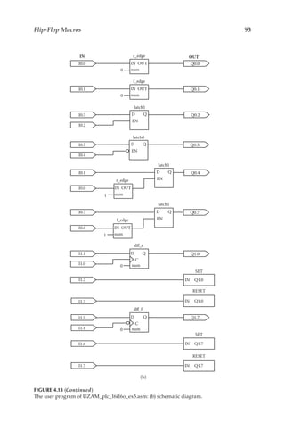
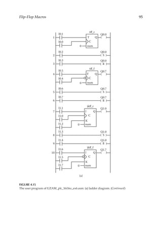
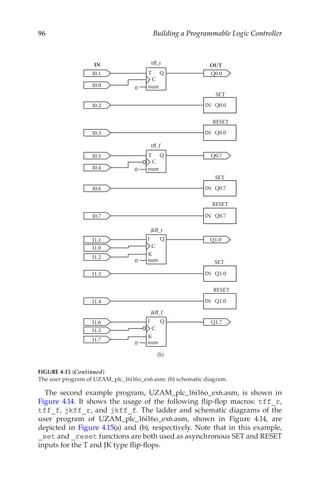
4. Flip-flop macros: The following flip-flop–based macros are
described in this chapter: r_edge (rising edge), f_edge (falling
edge), latch0, latch1, dff_r (rising edge triggered D flip-flop),
dff_f (falling edge triggered D flip-flop), tff_r (rising edge trig-
gered T flip-flop), tff_f (falling edge triggered T flip-flop), jkff_r
(rising edge triggered JK flip-flop), and jkff_f (falling edge trig-
gered JK flip-flop).
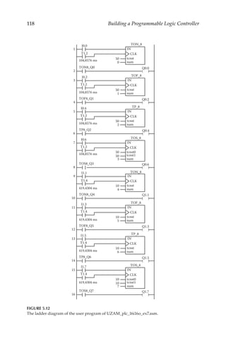
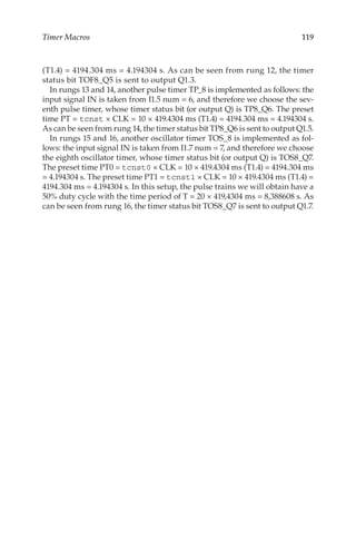
5.
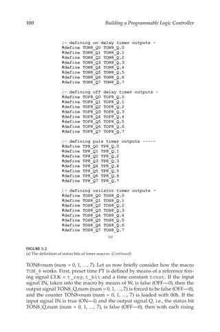
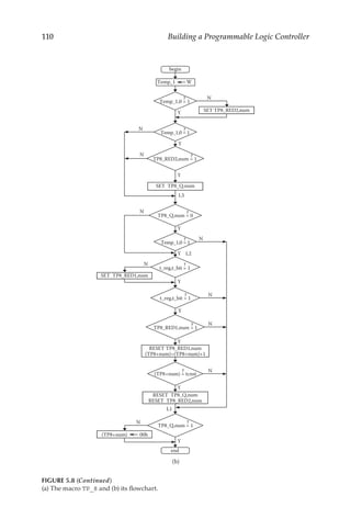
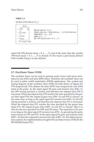
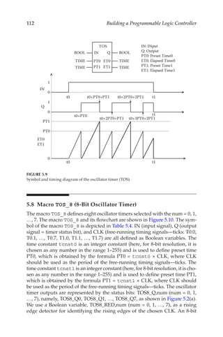
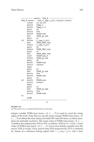
Timer macros: The following timer macros are described in this
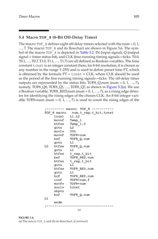
chapter: TON_8 (8-bit on-delay timer), TOF_8 (8-bit off-delay timer),
TP_8 (8-bit pulse timer), and TOS_8 (8-bit oscillator timer).
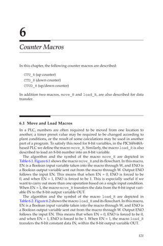
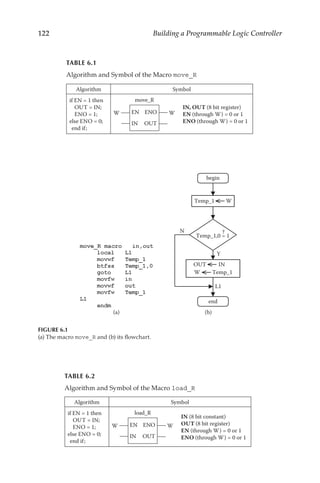
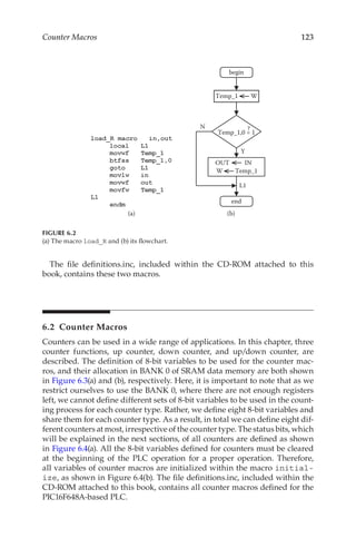
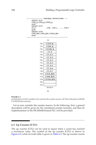
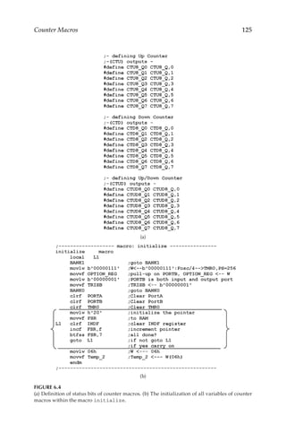
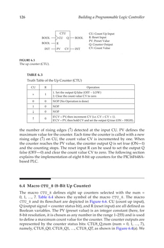
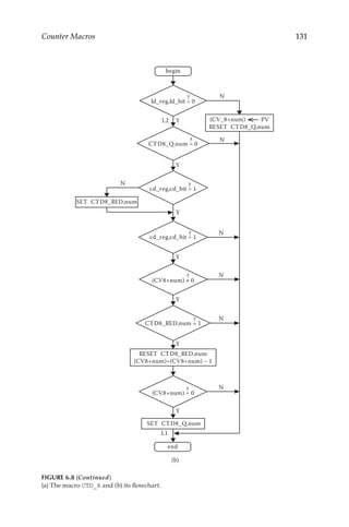
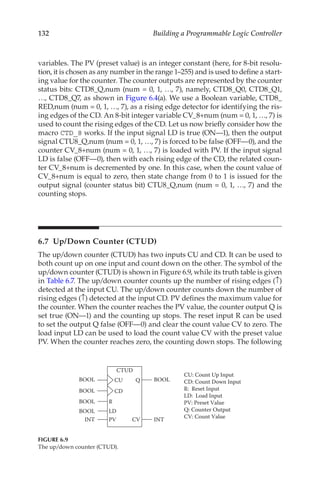
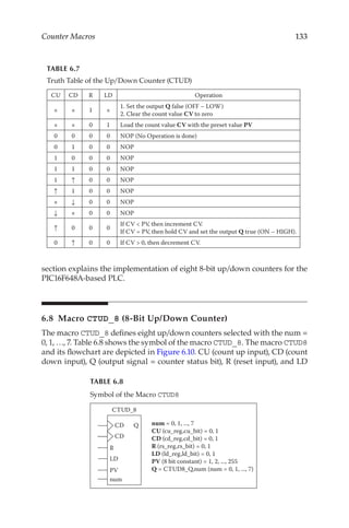
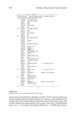
6. Counter macros: The following counter macros are described in this
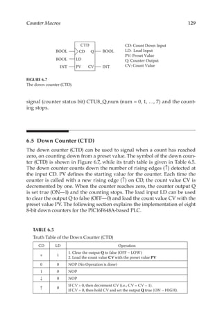
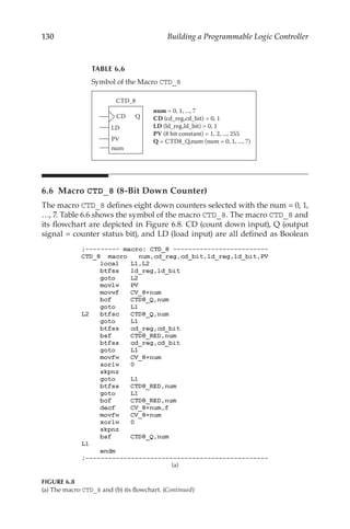
chapter: CTU_8 (8-bit up counter), CTD_8 (8-bit down counter), and
CTUD_8 (8-bit up/down counter).](https://image.slidesharecdn.com/buildingaprogrammablelogiccontrollerwithapic16f648amicrocontrollerlenguajeasembler-220618154203-89548f6a/85/Building-a-Programmable-Logic-Controller-with-a-PIC16F648A-Microcontroller-lenguaje-asembler-pdf-19-320.jpg)
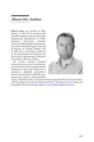
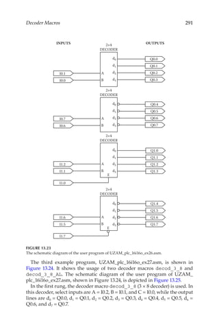
![xx Background and Use of the Book
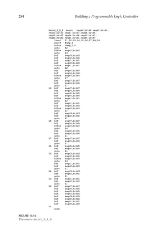
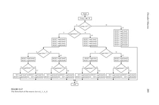
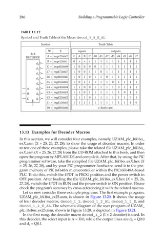
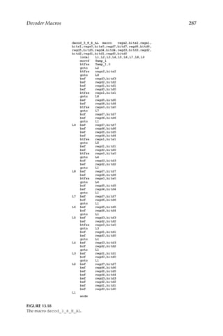
decod_3_8_E_AL (3×8 decoder with enable input and active low
outputs).
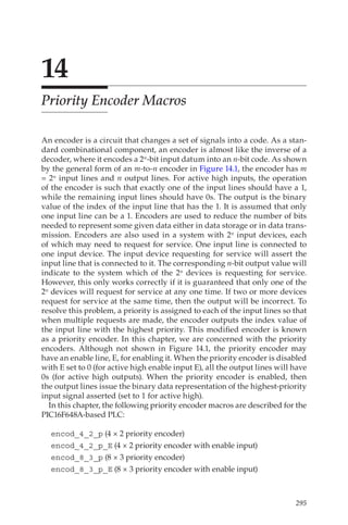
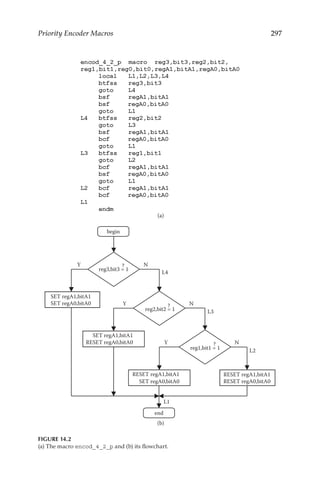
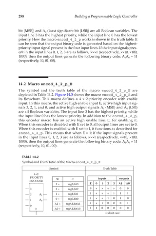
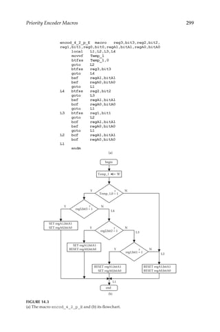
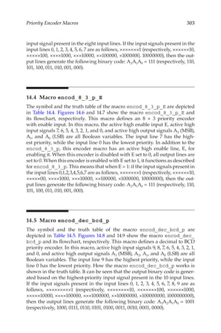
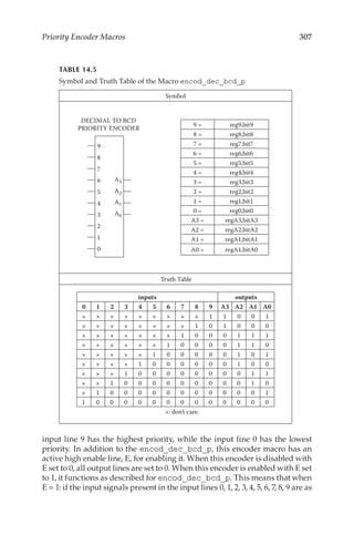
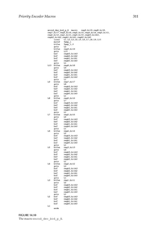
14. Priority encoder macros: The following priority encoder mac-
ros are described in this chapter: encod_4_2_p (4×2 priority
encoder), encod_4_2_p_E (4×2 priority encoder with enable
input), encod_8_3_p (8×3 priority encoder), encod_8_3_p_E
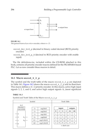
(8×3 priority encoder with enable input), encod_dec_bcd_p
(decimal to binary coded decimal [BCD] priority encoder), and
encod_dec_bcd_p_E (decimal to BCD priority encoder with
enable input).
15. Application example: This chapter describes an example remotely
controlled model gate system and makes use of the PIC16F648A-
based PLC to control it for different control scenarios.
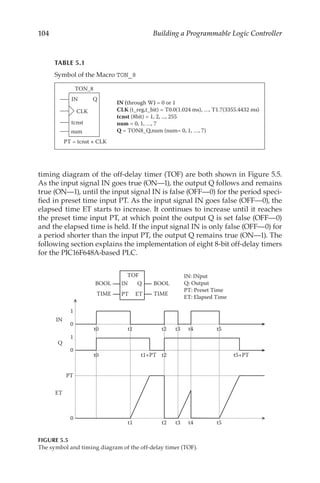
Table 1 shows the general characteristics of the PIC16F648A-based PLC.
TABLE 1
General Characteristics of the PIC16F648A-Based PLC
Inputs/Outputs/Functions
Byte Addresses/
Related Bytes
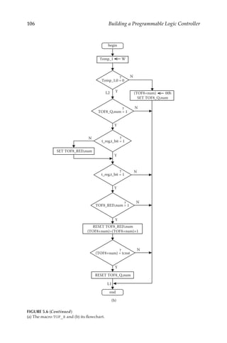
Bit Addresses or Function
Numbers
16 discrete inputs
(external inputs: 5 or 24 V DC)
I0
I1
I0.0, I0.1, …, I0.7
I1.0, I1.1, …, I1.7
16 discrete outputs
(relay type outputs)
Q0
Q1
Q0.0, Q0.1, …, Q0.7
Q1.0, Q1.1, …, Q1.7
32 internal relays
(memory bits)
M0
M1
M2
M3
M0.0, M0.1, …, M0.7
M1.0, M1.1, …, M1.7
M2.0, M2.1, …, M2.7
M3.0, M3.1, …, M3.7
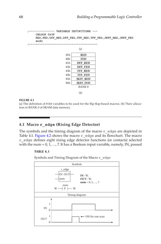
8 rising edge detectors RED r_edge (0, 1, …, 7)
8 falling edge detectors FED f_edge (0, 1, …, 7)
8 rising edge triggered
D flip-flop
DFF_RED
dff_r (0, 1, …, 7), regi,biti,
rego,bito
8 falling edge triggered
D flip-flop
DFF_FED
dff_f (0, 1, …, 7), regi,biti,
rego,bito
8 rising edge triggered
T flip-flop
TFF_RED
tff_r (0, 1, …, 7), regi,biti,
rego,bito
8 falling edge triggered
T flip-flop
TFF_FED
tff_f (0, 1, …, 7), regi,biti, rego,bito
8 rising edge triggered
JK flip-flop
JKFF_RED
jkff_r (0, 1, …, 7), regi,biti,
rego,bito
8 falling edge triggered
JK flip-flop
JKFF_FED
jkff_f (0, 1, …, 7), regi,biti,
rego,bito](https://image.slidesharecdn.com/buildingaprogrammablelogiccontrollerwithapic16f648amicrocontrollerlenguajeasembler-220618154203-89548f6a/85/Building-a-Programmable-Logic-Controller-with-a-PIC16F648A-Microcontroller-lenguaje-asembler-pdf-21-320.jpg)


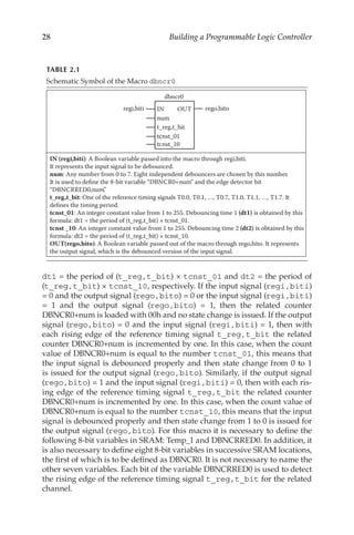
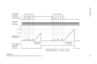
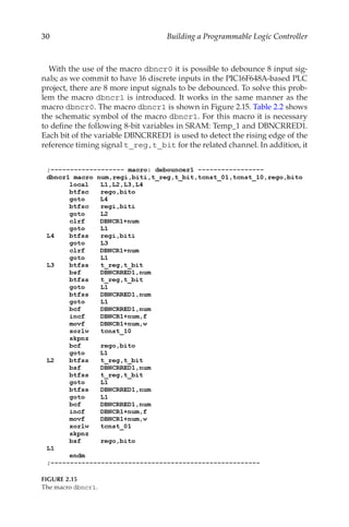


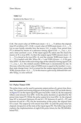
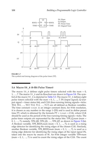

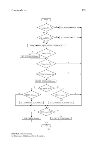
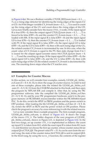
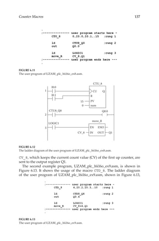
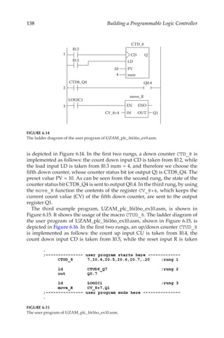
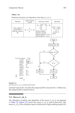
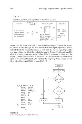
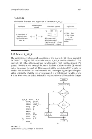
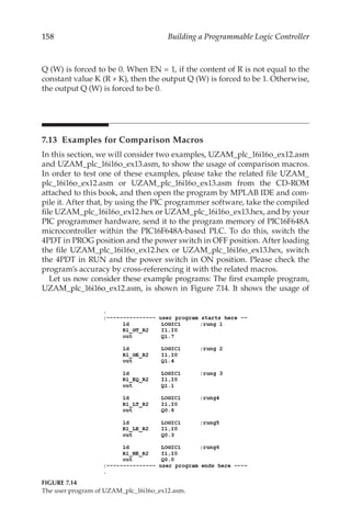
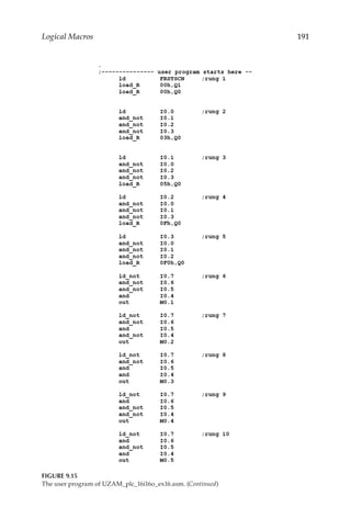
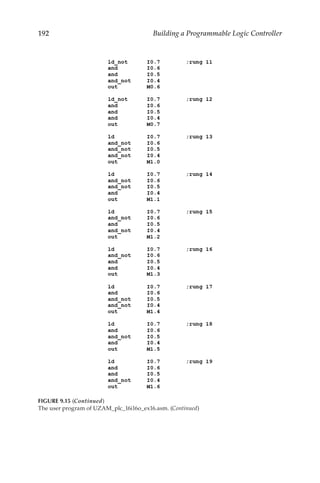
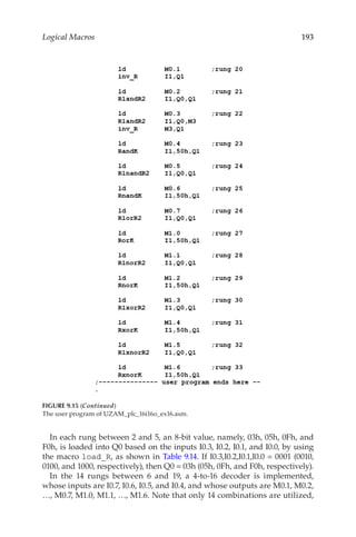
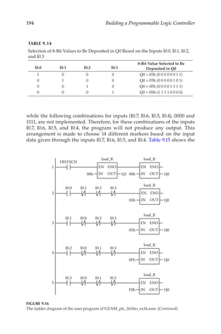


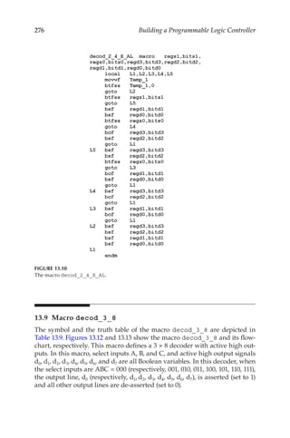
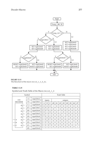
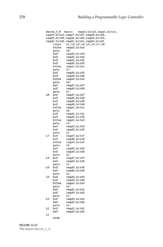
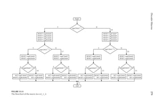


This document provides an overview of a book that describes how to build a programmable logic controller (PLC) using a PIC16F648A microcontroller. The book teaches advanced students and engineers how to design and use a microcontroller-based PLC. It assumes the reader has knowledge of digital logic, microcontrollers, and PLCs. The accompanying CD-ROM contains all the source code and examples from the book. The goal is to answer how one can design and implement a PLC in a way that is accessible for learning.


![[Deck] What's New in Spark-Iceberg Integration via DSV2.pptx](https://cdn.slidesharecdn.com/ss_thumbnails/deckwhatsnewinspark-icebergintegrationviadsv2-260210005337-25955b12-thumbnail.jpg?width=640&height=640&fit=bounds)


