More Related Content
Similar to BN hybridezed graphene
Similar to BN hybridezed graphene (20)
BN hybridezed graphene
- 1. ARTICLES
PUBLISHED ONLINE: 28 FEBRUARY 2010 | DOI: 10.1038/NMAT2711
Atomic layers of hybridized boron nitride and
graphene domains
Lijie Ci1 *, Li Song1 *, Chuanhong Jin2 , Deep Jariwala1† , Dangxin Wu3 , Yongjie Li1† , Anchal Srivastava1† ,
Z. F. Wang3 , Kevin Storr4 , Luis Balicas5 , Feng Liu3 and Pulickel M. Ajayan1‡
Two-dimensional materials, such as graphene and monolayer hexagonal BN (h-BN), are attractive for demonstrating
fundamental physics in materials and potential applications in next-generation electronics. Atomic sheets containing
hybridized bonds involving elements B, N and C over wide compositional ranges could result in new materials with properties
complementary to those of graphene and h-BN, enabling a rich variety of electronic structures, properties and applications.
Here we report the synthesis and characterization of large-area atomic layers of h-BNC material, consisting of hybridized,
randomly distributed domains of h-BN and C phases with compositions ranging from pure BN to pure graphene. Our studies
reveal that their structural features and bandgap are distinct from those of graphene, doped graphene and h-BN. This new form
of hybrid h-BNC material enables the development of bandgap-engineered applications in electronics and optics and properties
that are distinct from those of graphene and h-BN.
R
ecent investigations have demonstrated that graphene has structures. h-BN is a material with a wide bandgap of up to 5.9 eV,
spectacular electronic properties1 . Various approaches have with important applications as a deep-ultraviolet-light emitter16,17 .
been developed to fabricate high-performance graphene We expect that the hybridized h-BNC structures would have
devices by engineering their bandgaps so as to improve their interesting properties by combining the properties of two seemingly
semiconducting properties. One of the most feasible methods disparate materials with similar lattice parameters and crystal
to control the semiconducting properties of graphene is by structure. Here we show that we have successfully synthesized
doping, which is a process intentionally used to tailor the uniform and continuous h-BNC films on a large area.
electrical properties of intrinsic semiconductors. Experimental and To synthesize h-BNC films, we used a thermal catalytic CVD
theoretical studies on graphene doping show the possibility of method (see Supplementary Information for more details), which
making p-type and n-type semiconducting graphene by substituting has the potential for large-wafer growth of graphene18 . We chose
C atoms with B and N atoms2–4 , respectively. The dopant atoms Cu as substrate, which has been successfully used for large-area
can modify the electronic band structure of graphene, and open graphene growth19 . Cu substrates have also been used previously
up an energy gap between the valence and conduction bands. More for h-BN deposition20 . A surface-adsorption growth mechanism
interestingly, B, C and N can be atomically mixed together to form has recently been proposed for graphene deposition on a Cu
various semiconducting hexagonal layered structures with varying surface21 , implying that if we simultaneously supply a C and a
stoichiometry, such as BCN nanotubes5,6 . BCN graphitic films BN source it may be possible to deposit two-dimensional (2D)
(thickness from 100 nm to a few micrometres) have been prepared monolayers of h-BNC. In our growth, methane and ammonia
by thermally decomposing B-, C- and N-containing precursors by borane (NH3 –BH3 ) were used as precursors for carbon and BN,
chemical vapour deposition (CVD; ref. 7). Experimental studies and respectively. The atomic ratio of B, C and N can be tuned by
theoretical calculations have indicated that BCN nanostructures controlling the experimental parameters, although the B/N ratio is
show semiconducting properties with a small bandgap7–9 and always unity. For example, we can control the atomic percentage
interesting mechanical properties10 . of C from about 10% to ∼100% (see Supplementary Table S1).
Previous studies have found that B–N and C–C bonds tend to After growth, the films were transferred to other substrates for
segregate in the BCN systems11 . For example, owing to their very further characterization (see Supplementary Fig. S1a,b). Similar
similar lattice parameters, it is possible to synthesize layer-by-layer to the processing of graphene, the h-BNC films could also be
composite structures of hexagonal BN (h-BN) and graphene12–14 . lithographically patterned and cut into various shapes by exposure
Theoretical calculations indicate that a small bandgap can be in oxygen plasma (see Supplementary Fig. S1c). This enables
opened by placing a graphene layer onto an h-BN substrate15 . h-BNC atomic films to be easily fabricated into devices. Figure 1a
A hybrid atomic monolayer consisting of hybridized phases of is a photograph of h-BNC film on a quartz substrate, showing
h-BN and graphene (h-BNC) is another interesting structure that that the film is transparent. Figure 1b shows an atomic force
would enable the tailoring of physical properties in graphene-based microscopy (AFM) image of the film on a Si substrate. Both optical
1 Department of Mechanical Engineering & Materials Science, Rice University, Houston, Texas 77005, USA, 2 Nanotube Research Center, National Institute
of Advanced Industrial Science and Technology (AIST), Tsukuba 305-8565, Japan, 3 Department of Materials Science & Engineering, University of Utah,
Salt Lake City, Utah 84112, USA, 4 Department of Physics, Prairie View A&M University, Prairie View, Texas 77446, USA, 5 National High Magnetic Field
Laboratory, Tallahassee, Florida 32310, USA. *These authors contributed equally to this work. † Present addresses: Department of Metallurgical
Engineering, Banaras Hindu University, Varanasi 221005, India (D.J.); Department of Physics, Banaras Hindu University, Varanasi 221005, India (A.S.);
Department of Chemistry, Lanzhou University, Lanzhou 730000, China (Y.L.). ‡ e-mail: ajayan@rice.edu.
NATURE MATERIALS | ADVANCE ONLINE PUBLICATION | www.nature.com/naturematerials 1
© 2010 Macmillan Publishers Limited. All rights reserved.
- 2. ARTICLES NATURE MATERIALS DOI: 10.1038/NMAT2711
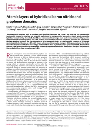
a b
h-BNC film
c d e
CK
4
σ∗
3
Counts (× 105)
2
BK π∗
NK
σ∗ π∗ σ∗
1
π∗
0
200 300 400
Energy loss (eV)
Figure 1 | Characteristics of an h-BNC film. a, Photograph of a transparent h-BNC film on a quartz slide. b, An AFM image shows the uniform thickness of
an h-BNC film (scale bar: 1 µm). c,d, HRTEM images indicate that the as-grown films are two or three atomic layers thick (scale bars: 5 nm). e, K-shell
excitations of B, C and N are revealed from the core EELS spectra taken from these films.
imaging and AFM images indicate that the film is fairly uniform be resolved from the hexagonal packing, we have not been able
except for some wrinkles. Further AFM thickness measurement to identify the positions of the individual B, C and N atoms in
indicates that the thickness of the films is about 1 nm (see the lattice, owing to their very close atomic sizes. Atomic HRTEM
Supplementary Fig. S2). High-resolution transmission electron images and selected-area electron diffraction patterns taken from
microscopy (HRTEM) observations indicate that our h-BNC films several areas show more details of our few-layer h-BNC films
mainly consist of two or three layers, as Fig. 1c,d shows. This is (see Supplementary Figs. S4,S5). We find that the multiple layers
slightly different from the growth of graphene on Cu, which leads are typically in turbostratic stacking and that the different Moiré
mainly to the growth of a single layer under similar conditions19 . patterns seen in the atomic-scale images are due to the lack of AB
We made electron energy-loss spectroscopy (EELS) measure- stacking registry between the layers24 . Figure 2b shows an image of
ments on the h-BNC film to determine their chemical composi- such a Moiré pattern, and the FFT pattern shown in the inset shows
tion and structure. Figure 1e shows an EELS spectrum with three three sets of hexagonal spots with a rotational angle of 11◦ , which
visible edges starting at 185, 276 and 393 eV, corresponding to the indicates that this is a three-layer region, and the relative rotational
characteristic K-shell ionization edges of B, C and N, respectively22 . angle with respect to each layer is 11◦ . Figure 2c shows an area with a
The three bands corresponding to each element can be well resolved different Moiré pattern, and the FFT pattern, as shown in the inset,
and show a first peak corresponding to the 1s-π ∗ antibonding orbit, indicates a two-layer stacking with a relative rotational angle of 16◦ .
followed by a wider band attributed to the 1s-σ ∗ antibonding orbit. Using the FFT spots, we can reconstruct each sheet of the hexagonal
This type of EELS edge structure proves that all three elements are atomic network, as shown in Fig. 2d,e (see Supplementary Fig. S6
sp2 hybridized22,23 , and indicates that the atomic films grown on Cu for more details). The hexagonal atomic arrangement can be clearly
possess a hexagonal structure consisting of B, C and N. Elemen- identified from the reconstructed images. A proposed model for
tal mapping using energy filtered techniques (see Supplementary the structure of our atomic films based on hybridized domains
Fig. S3) also proves that all three elements are distributed over the of h-BN and C is shown in Fig. 2f. The model is based on our
entire area of the films. Using a low-voltage aberration-corrected experimental analysis (the following sections and Supplementary
HRTEM, we show the atomic structure of our as-grown h-BNC Fig. S10 in Section S6) and theoretical calculations on the stability
film (Fig. 2). As mentioned above, most of our h-BNC films are two of h-BNC films (see more details in Supplementary Section S5).
or three layers thick. However, we can expose small areas showing Figure 3a–c shows an X-ray photoelectron spectroscopy (XPS)
projections from a single layer only (Fig. 2a), so that the atomic spectrum of B, N and C, respectively, from an as-grown h-BNC
structure of an individual layer can be observed. The inset of Fig. 2a, film. The shape and position of the spectra of all three elements
showing the fast Fourier transform (FFT) from the image, indicates are very different from those of previous XPS studies of films
a hexagonal atomic structure. Even though individual atoms can with BC2 N and BCN compositions9,25 . The main peak of the B 1s
2 NATURE MATERIALS | ADVANCE ONLINE PUBLICATION | www.nature.com/naturematerials
© 2010 Macmillan Publishers Limited. All rights reserved.
- 3. NATURE MATERIALS DOI: 10.1038/NMAT2711 ARTICLES
a b
11°
11°
c d f
16°
e
B C N
Figure 2 | Atomic HRTEM images of h-BNC film. a, An HRTEM image of a single-layer region exposed a nearby hole in the film. The inset is the FFT
pattern of the single-layer region. b, An atomic-scale Moiré pattern; the inset FFT indicates a three-layer stacked region with rotational angle of 11◦ . c, A
Moiré pattern from a different region; the FFT in the inset reveals a two-layer packing with a relative rotational angle of 16◦ . d,e, Two individual atomic
layers reconstructed by masking the FFT pattern from the area in c (red line). f, Atomic model of the h-BNC film showing hybridized h-BN and graphene
domains. Scale bars: 2 nm.
spectrum is at 190.9 eV (Fig. 3a), which is very close to that of B 1s broader D band at 1,360 cm−1 . At 1,620 cm−1 (D band), a shoulder
(190.1 eV) in h-BN (ref. 9). This suggests that the main bonding appears on the right side of the G band. Both Raman D and D
configuration for B in our films is similar to that of h-BN, where bands of carbon materials originate from the finite crystal size or
three N atoms surround one B atom. However, a small shoulder lattice distortion26 . The second-order Raman band located at about
at a lower binding energy of 188.4 eV implies a contribution from 2,700 cm−1 (2D band) has been used to determine the number of
the bonding configurations of B and C, and this is because C atoms layers of CVD-grown graphene according to its relative intensity
have a lower electronegativity than N (ref. 25). The N 1s peak is with respect to the G band and its position18,19 . The intensity of
located at 398.0 eV (Fig. 3b), similar to the position of the N 1s the 2D band from the pure graphene is about twice that of the
spectrum (398.1 eV) of h-BN (ref. 9). However, the shoulder seen at G band, indicating one to two layers of graphene. For bilayer or
the higher energies suggests that some N atoms partially bond with trilayer pure graphene, the intensity of the 2D band is supposed
C atoms. Both the B 1s and the N 1s spectrum indicate that the main to be equal to that of the G band. However, in the h-BNC film
configuration for B and N atoms is the B–N bond, implying that (2–3 layers), the intensity of the 2D band is suppressed, possibly
h-BN domains exist in the film. The C 1s peak is located at 284.4 eV owing to a strong photoluminescence background. Our Raman data
(Fig. 3c), which is close to the value observed in graphite (284.9 eV). support the model of domain structure (Fig. 2f) in our h-BNC films.
This suggests that the C–C bonds stay together and form graphene For example, if they were h-BN/graphene stacked structures, as we
domains. The small shoulder at the higher binding energies is due did not see apparent Raman signal from our CVD-grown pure BN,
to C–N bonds, whereas the other one at lower binding energies is the Raman spectrum should be very close to that of graphene. We
from C–B bonds. These bonds must be located at the boundaries should observe a lower D peak at 1,340 cm−1 and a higher and
of the hybridized h-BN and graphene domains, as shown in the narrower G peak at 1,580 cm−1 , and a 2D peak at around 2,700 cm−1
atomic model in Fig. 2f. should provide us with information about the formation of single-
Figure 3d shows a typical Raman spectrum of the h-BNC atomic or bilayer graphene. Experimentally, we can tune the compositional
film (top curve). Compared with that of a pure graphene sample ranges of the two components (C and BN) over the whole range, a
(bottom curve), the h-BNC curve shows a much higher and fact that also does not support a BN/graphene stacked structure (for
NATURE MATERIALS | ADVANCE ONLINE PUBLICATION | www.nature.com/naturematerials 3
© 2010 Macmillan Publishers Limited. All rights reserved.
- 4. ARTICLES NATURE MATERIALS DOI: 10.1038/NMAT2711
a d 2D
h-BNC
B 1s
Intensity (a.u.)
G
D'
D
Intensity (a.u.)
186 188 190 192 194 196
Binding energy (eV)
b Graphene
N 1s
Intensity (a.u.)
1,200 1,400 1,600 2,600 2,800
Raman shift (cm¬1)
e
396 398 400 402 0.16
Binding energy (eV)
Absorpance (a.u.)
c 0.12
C 1s
Intensity (a.u.)
0.08
0.04
h -B
800 NC
h-B 85
280 282 284 286 288 290 600 NC at.%
Wa Gra 65 C
vele phe at.%
Binding energy (eV) ngt 400 Pur ne C
h (n e h-
m) 200 BN
Figure 3 | Evidence for hybridized h-BN and graphene domain-like structure of h-BNC. a–c, XPS spectra of B, N and C 1s core levels, respectively. The
spectrum curves (filled diamonds) are deconvoluted (black dashed curves) by Gaussian fitting (red curves), indicating possible multibonding information.
d, Raman spectrum of an h-BNC and a CVD-grown graphene film. e, Ultraviolet–visible absorption spectra of different graphene films.
example, a two-layer film should be restricted to 50 at.% carbon). resume their individual bandgap identities, forming effectively a
We can conclude that both Raman D and D bands should be mainly superlattice. This provides further evidence that the film we have
attributed to disorders and boundaries in the carbon network made consists of hybrid atomic layers of h-BN and C graphene
induced by BN domains. nanodomains rather than a substitutionally doped (B and N in C)
The ultraviolet–visible absorption spectrum was taken to or alloyed phase between h-BN and pure graphene.
investigate the optical energy gap of the h-BNC film owing to To investigate electrical properties of the h-BNC films, devices
optically induced transitions. The optical bandgaps are determined with four electrodes were fabricated (see Fig. 4a, and also
on the basis of Tauc’s formulation27 . As Fig. 3e shows, a graphene Supplementary Fig. S8a,b). Figure 4b shows the linear I –V
sample shows a very weak absorption edge in the range of behaviour from all the samples. We found that the electrical
190–800 nm. The absorption spectrum of the h-BN sample shows conductivity of h-BNC ribbon increases on increasing its percentage
one absorption edge at 218 nm, which corresponds to an optical of carbon. The pure BN film is an insulator, whereas the h-BNC
bandgap of 5.69 eV (see Supplementary Fig. S7 for the method). ribbon with 94% carbon has a lower resistivity, around 10−3 cm.
Absorption curves from h-BNC films show two absorption edges, This suggests that we can easily control the electrical properties of
indicating two possible domain structures as proposed. For the our h-BNC films from insulator to highly conducting by tuning the
h-BNC sample with 65 at.% C, the first absorption edge corresponds carbon concentration. Figure 4c shows the back-gate-dependent
to an optical bandgap of 4.48 eV, which must come from h-BN electrical response of an h-BNC sample (40 at.% C) at room
domains in the film. However, it is smaller than that of h-BN sample temperature. The drain current is modulated by applying a gate
(5.69 eV), indicating the effect of C doping. There may be some voltage. Our h-BNC field-effect transistor shows an ambipolar
intrinsic doping (C atom in BN or B, N in graphene domain) semiconducting behaviour, which is similar to that of CVD-grown
or a boundary effect, which are difficult to distinguish from each graphene17–19 . This result further indicates that our films have
other. We can see that increasing C content to 84 at.% lowers an atomic structure consisting of hybridized h-BN and graphene
this value to 3.85 eV. The second absorption edge corresponds domains, because theoretical and experimental investigations have
to an optical bandgap of 1.62 eV and 1.51 eV from the samples indicated that B, C, N mixed atomic structures are typically p-type
with 65 at.% C and 84 at.% C, respectively. This absorption edge semiconductors29,30 . The h-BN domains decrease the gating effect,
must be from h-BN-doped graphene domains. On the basis of the which results in a lower effective gate modulation behaviour. We
measured bandgaps, we expect the domain size to be larger than a calculate the carrier mobility from the slope of the conductivity
few nanometres (see Supplementary S6). If all the domain sizes were variation with gate voltage. The electron and hole mobility of our
smaller than 2–3 nm, then the film would behave like a BN–C ‘alloy’, h-BNC devices is in the range of 5–20 cm2 V−1 s−1 . This value
with a bandgap equal to the average gap of h-BN and graphene, is much smaller than the mobilities reported for graphene17,19 ,
similar to the case of a short-period semiconductor superlattice28 . and can be attributed to electron scattering at the boundaries
The fact that we observe two different optical bandgaps indicates between h-BN and graphene domains inside the sample. The
that both the h-BN and graphene domains are large enough to carrier scattering also induces a charge-neutrality point (point of
4 NATURE MATERIALS | ADVANCE ONLINE PUBLICATION | www.nature.com/naturematerials
© 2010 Macmillan Publishers Limited. All rights reserved.
- 5. NATURE MATERIALS DOI: 10.1038/NMAT2711 ARTICLES
a b 30
100 at.% C
25
20 94 at.% C
Drain current (μA)
15
10 56 at.% C
5
35 at.% C
0
h-BN
0 0.2 0.4 0.6 0.8 1.0
Drain voltage (V)
c 5.6 d
3.0 16
5.2 2.5 15 Eg = 18.19 meV
Drain current (× 10¬6 A)
Vsd = 1 V
Resistance (× 106 Ω )
ln (R)
2.0 14
4.8
1.5 13
4.4
12
1.0 0.010 0.015 0.020
4.0 0.5 1/T (K¬1)
3.6 0
¬40 ¬20 0 20 40 50 100 150 200
Back-gate voltage (V) Temperature (K)
Figure 4 | Electrical properties of h-BNC atomic films. a, Optical image of a four-terminal h-BNC ribbon field-effect transistor. Scale bar: 30 µm.
b, Current–voltage (I–V) characteristics of as-grown BNC with different percentages in carbon measured at room temperature. c, The drain current
as a function of the voltage applied to the back gate for a 7-µm-wide BNC ribbon with 40% carbon. The drain–source voltage is fixed to 1 V.
d, A resistance-versus-temperature curve for a typical h-BNC ribbon with a width of 5 µm and a length of 11 µm. The inset shows ln(R) as a function of T −1
in the temperature range from 50 to 100 K. The linear fit (solid line) shows that the data are well described by R(T) ∝ exp(E /kB T). E is the bandgap and
kB is Boltzmann’s constant.
minimum conductivity) shifting up to a gate voltage of 18 V (ref. 31) Fig. S9a,b). Using the tight-binding method, we estimated an upper
(see Supplementary Fig. S8c for more neutrality-point shifts at limit of the domain size for the film with 50 at.% C to be ∼42 nm
various carbon percentages). We would like to point out here that from the measured gap of 18 meV (see Supplementary Fig. S9c).
the above electrical transport data do not support a C/BN stacked Our modelling indicates that the experimentally observed h-BNC
structure: otherwise, the conductivity should be dominated by the must be a kinetically stabilized non-equilibrium-grown structure
highly conducting graphene layer. where the actual domain size could be controlled by various kinetic
Temperature-dependent electrical transport measurements on factors, such as the growth temperature, the deposition rate and the
our h-BNC samples (Fig. 4d) show a significant increase in the effect of the substrate.
resistance by more than 10-fold on cooling down from room We have synthesized a new form of 2D atomic film consisting
temperature to 50 K, which is a typical semiconducting behaviour. of hybridized h-BN and C (graphene) domains, showing structural
The value of the bandgap is calculated on the basis of a linear features and a bandgap that have not been found in graphene, h-BN
Arrhenius plot of the logarithm of the resistance ln(R) versus the or boron- and nitrogen-codoped graphene. This new structure with
inverse temperature T −1 (see Fig. 4d, inset). The measured bandgap separated graphene and BN domains and a wide range of com-
is 18 meV for a 5-µm-wide h-BNC ribbon with 56 at.% carbon, and positions may be engineered to build unique semiconducting 2D
this value for the bandgap is close to that of a 30-nm-wide pristine architectures, which could have potential applications in electronics
graphene ribbon32 . As discussed above, the h-BNC samples consist and optics. These hybridized atomic films are an isotropic structure,
of a percolating graphene network embedded with BN domains. and we did not observe any anisotropic property in our electrical
As the BN domains have a very large bandgap (∼5 eV) acting like transport or optical results. In addition, the h-BN domains can act
an ‘infinite’ barrier, the electronic and transport properties of the as long-range impurities within the graphene lattice, making h-BNC
graphene network will be similar to those of the graphene nanohole a promising system for fundamental physical investigations, such as
superlattices33 . Small gaps are opened in the graphene owing to charge localization35 and possible metal–insulator transitions36 .
quantum confinement and/or spin polarization at specific C–BN
boundaries (see Supplementary Fig. S9c). Methods
First-principles calculations on the basis of the density functional CVD growth process. Growth of boron-nitride-hybridized graphene (h-BNC)
theory were carried out to model the h-BNC structure. Our was carried out in a split tube furnace with a fused-quartz processing tube (50 mm
modelling results, as well as recent reports34 , indicate that BN and outer diameter). Boron and nitrogen were introduced into the system by separately
C are thermodynamically immiscible, preferring to separate into heating ammonia borane using a heating belt in the front region of the processing
tube. The Cu substrate was placed in the furnace under vacuum, annealed at 600 ◦ C
2D domains in planar h-BNC structures. However, our calculations for 20 min in Ar/H2 (15 vol% H2 ) flow and gradually heated up to 900–1,000 ◦ C
also indicate that larger domains would be preferred to decrease the in 40 min. Methane and ammonia borane were then introduced into the growth
total domain interfacial energy in the system (see Supplementary chamber. During the growth process, Ar/H2 flow was shut down, and the system
NATURE MATERIALS | ADVANCE ONLINE PUBLICATION | www.nature.com/naturematerials 5
© 2010 Macmillan Publishers Limited. All rights reserved.
- 6. ARTICLES NATURE MATERIALS DOI: 10.1038/NMAT2711
vacuum was controlled by the methane flow (about 200 mtorr). The growth of 19. Li, X. et al. Large-area synthesis of high-quality and uniform graphene films on
pure h-BN and graphene films was also carried out without methane flow and BN copper foils. Science 324, 1312–1314 (2009).
introduction, respectively. 20. Preobrajenski, A. B., Vinogradov, A. S. & Mårtensson, N. Monolayer of h-BN
chemisorbed on Cu(111) and Ni(111). Surf. Sci. 582, 21–30 (2005).
Characterization methods. HRTEM, selected-area electron diffraction, EELS 21. Li, X., Cai, W., Colombo, L. & Ruoff, R. S. Evolution of graphene growth on
measurements and elemental mapping (Gatan GIF) were carried out on a Cu and Ni studied by carbon isotope labeling. Nano Lett. 9, 4268–4272 (2009).
JEOL-2100 field emission HRTEM operated at 200 kV. Atomically resolved 22. Stephan, O. et al. Doping graphitic and carbon nanotube structures with boron
HRTEM observations were conducted within a TEM set-up (JEOL-2010F, operated and nitrogen. Science 266, 1683–1685 (1994).
at 120 and 80 kV) equipped with a postspecimen aberration corrector (CEOS). 23. Kouvetakis, J. et al. Novel aspects of graphite intercalation by fluorine and
XPS (PHI Quantera XPS) was carried out using monochromatic aluminium Kα fluorides and new B/C, C/N and B/C/N materials based on the graphite
X-rays. XPS data were analysed with the MultiPak software. Raman spectroscopy network. Synth. Met. 34, 1–7 (1989).
(Renishaw inVia) was used to characterize the structure of the film at 514.5 nm 24. Warne, J. H., Rümmeli, M. H., Gemming, T., Büchner, B. & Briggs, G. A. D.
laser excitation. Optical-absorptance measurements (Shimadzu ultraviolet-3600) Direct imaging of rotational stacking faults in few layer graphene. Nano Lett. 9,
were made on atomic films after they were transferred onto optical quartz plates. 102–106 (2009).
The as-grown h-BNC film was transferred onto an n-type silicon wafer with a 25. Watanabe, M. O., Itoh, S., Mizushima, K. & Sasaki, T. Bonding characterization
300-nm-thick SiO2 layer for the fabrication of a back-gated field-effect transistor. of BC2 N thin films. Appl. Phys. Lett. 68, 2962–2964 (1996).
Optical lithography and the oxygen-plasma-etching process were used to pattern 26. Pimenta, M. A. et al. Studying disorder in graphite-based systems by Raman
the thin film into long h-BNC ribbons with widths ranging from 5 to 15 µm. spectroscopy. Phys. Chem. Chem. Phys. 9, 1276–1291 (2007).
Electrodes (Au/Ti = 30 nm/3 nm) were patterned onto the h-BNC ribbon by 27. Tauc, J., Grigorovici, R. & Vancu, A. Optical properties and electronic structure
using optical lithography and e-beam evaporator techniques. A probe station of amorphous germanium. Phys. Status Solidi 15, 627–637 (1966).
was used to test the electrical properties of h-BNC at room temperature. All 28. Ihm, J. Effects of the layer thickness on the electronic character in GaAs–AlAs
of the reported electrical transport measurements were made in a 10−5 torr superlattices. Appl. Phys. Lett. 50, 1068–1070 (1987).
vacuum chamber. We further characterized the electrical properties of h-BNC 29. Watanabe, M. O., Itoh, S., Mizushima, K. & Sasaki, T. Electrical properties of
ribbon by investigating the temperature dependence of the resistance in a 3 He BC2 N thin films prepared by chemical vapour deposition. J. Appl. Phys. 78,
cryostat. The data were recorded by using a Lakeshore resistance bridge in a 2880–2882 (1995).
four-terminal configuration. 30. Watanabe, M. O., Itoh, S., Sasaki, T. & Mizushima, K. Visible-light-emitting
layered BC2N semiconductor. Phys. Rev. Lett. 77, 187–189 (1996).
Received 21 October 2009; accepted 27 January 2010; 31. Novoselov, K. S. et al. Electric field effect in atomically thin carbon films.
published online 28 February 2010 Science 306, 666–669 (2004).
32. Han, M. Y., Özyilmaz, B., Zhang, Y. & Kim, P. Energy band-gap engineering of
References graphene nanoribbons. Phys. Rev. Lett. 98, 206805 (2007).
1. Geim, A. K. & Novoselov, K. S. The rise of graphene. Nature Mater. 6, 33. Liu, W., Wang, Z. F., Shi, Q. W., Yang, J. & Liu, F. Band gap scaling of graphene
183–191 (2007). nanohole superlattices. Phys. Rev. B 80, 233405 (2009).
2. Wang, X. et al. N-doping of graphene through electrothermal reactions with 34. Yuge, K. Phase stability of boron carbon nitride in a heterographene structure.
ammonia. Science 324, 768–771 (2009). Phys. Rev. B 79, 144109 (2009).
3. Martins, T. B., Miwa, R. H., da Silva, A. J. R. & Fazzio, A. Electronic and 35. Carroll, D. L. Effects of nanodomain formation on the electronic structure of
transport properties of boron-doped graphene nanoribbons. Phys. Rev. Lett. doped carbon nanotubes. Phys. Rev. Lett. 81, 2332–2335 (1998).
98, 196803 (2007). 36. Zhang, Y. et al. Localization and the Kosterlitz–Thouless transition in
4. Lherbie, A., Blasé, R. X., Niquet, Y., Triozon, F. & Roche, S. Charge transport disordered graphene. Phys. Rev. Lett. 102, 106401 (2009).
in chemically doped 2D graphene. Phys. Rev. Lett. 101, 036808 (2008).
5. Cherrey, K. et al. Synthesis of Bx Cy Nz nanotubules. Phys. Rev. B 51, Acknowledgements
11229–11232 (1995). P.M.A. acknowledges support from Rice University start-up funds and funding
6. Golberg, D., Dorozhkin, P., Bando, Y. & Dong, Z. C. Synthesis, analysis and support from the Office of Naval Research (ONR) through the MURI programme on
electrical property measurements of compounds nanotubes in the ceramic graphene and the Basic Energy Sciences division of the Department of Energy (DOE).
B–C–N system. MRS Bull. 29, 38–42 (2004). L.C. (for work carried out on graphene growth and structural characterization) was
7. Kaner, R. B., Kouvetakis, J., Warble, C. E., Sattler, M. L. & Bartlett, N. supported by the ONR MURI programme (award No N00014-09-1-1066) and L.S.
Boron–carbon–nitrogen materials of graphite-like structure. Mater. Res. Bull. (for work done in device fabrication and electrical characterization) by DOE-BES
22, 399–404 (1987). programme DE-SC0001479. C.J. acknowledges the International Balzan Foundation
8. Liu, A. Y., Wentzcovitch, R. M. & Cohen, M. L. Atomic arrangement and for financial support through Meijo University. F.L. acknowledges support from
electronic structure of BC2 N. Phys. Rev. B 39, 1760–1765 (1989). DOE-BES programme DE-FG0203ER46027. Y.L. acknowledges a scholarship from
9. Miyamoto, Y., Rubio, A., Cohen, M. L. & Louie, S. G. Chiral tubules of the Chinese State Scholarship fund. A.S. acknowledges support from the BOYSCAST
hexagonal BC2 N. Phys. Rev. B 50, 4976–4979 (1994). scheme sponsored by the Department of Science and Technology (DST), India.
10. Hernández, E., Goze, C., Bernier, P. & Rubio, A. Elastic properties of C and K.S. acknowledges support from the National Science Foundation Major Research
Bx Cy Nz composite nanotubes. Phys. Rev. Lett. 80, 4502–4505 (1998). Instrumentation programme (NSF-MRI) DMR-0619801 (for the dilution refrigerator)
11. Kawaguchi, M., Kawashima, T. & Nakajima, T. Syntheses and structures of new and the Department of Energy National Nuclear Security Administration (DOE-NNSA)
graphite-like materials of composition BCN(h) and BC2 N(H). Chem. Mater. 8, DE-FG52-05NA27036 (17 T magnet and 3 He system) and the PVAMU Title III
1197–1201 (1996). Program US Department of Education (infrastructure). L.B. acknowledges support from
12. Suenaga, K. et al. Synthesis of nanoparticles and nanotubes with well-separated DOE-BES and NHMFL-UCGP programmes.
layers of boron nitride and carbon. Science 278, 653–655 (1997).
13. Han, W. Q., Mickelson, W., Cumings, J. & Zettl, A. Transformation of Bx Cy Nz
nanotubes to pure BN nanotubes. Appl. Phys. Lett. 81, 1110–1112 (2002).
Author contributions
L.C. and L.S. contributed equally to this work. L.C. and L.S. designed and carried out
14. Kawasaki, T. et al. Double atomic layers of graphene/monolayer h-BN on
most of the experiments (CVD, TEM, AFM, XPS, Raman, ultraviolet–visible spectra,
Ni(111) studied by scanning tunnelling microscopy and scanning tunnelling
electrical test), and analysed the data. C.J. carried out atomically resolved HRTEM
spectroscopy. Surf. Rev. Lett. 9, 1459–1464 (2002).
work. D.J. and A.S. conducted part of the CVD growth. Y.L. conducted part of the
15. Giovannetti, G., Khomyakov, P. A., Brocks, G., Kelly, P. J. & van den Brink, J.
XPS measurement. K.S., L.B. and L.S. conducted electrical measurements and data
Substrate-induced band gap in graphene on hexagonal boron nitride: Ab initio
analysis. D.W., Z.F.W. and F.L. carried out the modelling. P.M.A was responsible for
density functional calculations. Phys. Rev. B 76, 073103 (2007).
the project planning. L.C., L.S., P.M.A. and F.L. co-wrote the paper. All the authors
16. Watanabe, K., Taniguchi, T. & Kanda, H. Direct-band gap properties and
discussed the results.
evidence for ultraviolet lasing of hexagonal boron nitride single crystal.
Nature Mater. 3, 404–409 (2004).
17. Kubota, Y., Watanabe, K., Tsuda, O. & Taniguchi, T. Deep ultraviolet Additional information
light–emitting hexagonal boron nitride synthesized at atmospheric pressure. The authors declare no competing financial interests. Supplementary information
Science 317, 932–934 (2007). accompanies this paper on www.nature.com/naturematerials. Reprints and permissions
18. Reina, A. et al. Large area, few-layer graphene films on arbitrary substrates by information is available online at http://npg.nature.com/reprintsandpermissions.
chemical vapour deposition. Nano Lett. 9, 30–35 (2009). Correspondence and requests for materials should be addressed to P.M.A.
6 NATURE MATERIALS | ADVANCE ONLINE PUBLICATION | www.nature.com/naturematerials
© 2010 Macmillan Publishers Limited. All rights reserved.