2. observed for SuCoLEx. This opens ways to tailor thermal
expansion though strain engineering. To demonstrate the
performance of our composite as a heat-sink material, we show
that SuCoLEx reduces the thermal strain in silicon by up to a
factor of 4 compared to copper and aluminum and outperforms
copper in cooling a high-power light-emitting device (LED).
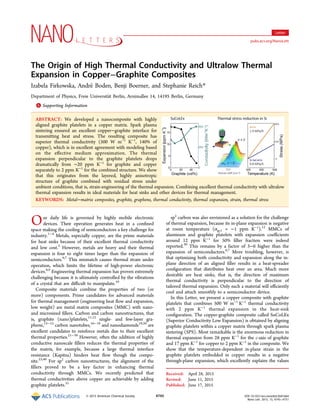
Graphite platelets with lateral size of 300 and 5 μm thickness
(Figure 1a) were mixed with copper powder by ball milling (see
Experimental Methods). The extracted material was consoli-
dated by SPS39,41,42
resulting in the metal−matrix composite
SuCoLEx that can be shaped, cut, and polished (Figure 1c).
This bulk synthesis approach is a big advantage for thermal
Figure 1. Structure and density of SuCoLEx. (a) Scanning electron microscopy (SEM) image of a graphite platelet. (b) SEM image of the SuCoLEx
cross-section. The arrow highlights the graphite alignment. (c) Density (black square) and expected density (dashed line) of SuCoLEx as well as
pictures of the bulk material compared to one cent. (d) Raman intensity of the G peak as a function of the angle between the polarization of the light
and in-plane direction of SuCoLEx for 8 (black square), 20 (red circle), 40 (green triangle), and 50 vol % (blue diamond).
Figure 2. Thermal properties of SuCoLEx. (a) Thermal conductivity of SuCoLEx in the in-plane kx (blue circle) and through-plane kz (black square)
direction obtained from the measured thermal diffusivity, density, and heat capacity (Supporting Information). Dashed lines were calculated with the
effective medium approximation and σG = 0.37 alignment. The right axis is the thermal conductivity enhancement (TCE, ratio between composite
and matrix thermal conductivity). (b) Through-plane αz (black square) and in-plane coefficient of thermal expansion αx (blue circle) of SuCoLEx.
The dotted and dashed lines are the modeling predictions. (c) Sandwich-like structure of copper and graphite.
Nano Letters Letter
DOI: 10.1021/acs.nanolett.5b01664
Nano Lett. 2015, 15, 4745−4751
4746
3. management applications over techniques that produce MMC
films.36−38
The addition of graphite to the copper matrix
reduced the density (Figure 1c) and increased the heat capacity
(Supporting Information Figure 1S) following the rule of
mixture. We characterized the nanofillers and the composite by
Raman scattering and electron microscopy. The crystalline
structure of the graphite platelets remained intact during
composite synthesis as verified by the constant D-line intensity
in Raman scattering (Supporting Information Figure 2S). The
internal structure of SuCoLEx shows strong alignment of the
graphite flakes, Figure 1b. This alignment occurs because of the
platelet geometry (small thickness to length ratio) combined
with the forces during consolidation. The thin graphite particles
orient during SPS, because it is performed under uniaxial
pressure, see Methods. The c-axis of the platelets is
preferentially oriented along the force direction, which we
call the through-plane direction or z-axis in this paper; compare
inset of Figure 2a. To quantify the platelet orientation, we
measured the Raman intensity of the G peak as a function of
the polarization angle of the incoming and scattered light
(Figure 1d).21,43
The intensity drop at 90° and 270° confirms
the alignment of the platelets, which is strongest for 40 and 50
vol % platelet concentration (further details can be found in
Supporting Information). We evaluated the polarization
dependent intensity following ref 21 and obtained a standard
distribution for the orientation σG = 0.69 for 8 vol %, σG = 0.61
for 20 vol %, and σG = 0.37 for a graphite volume fraction above
20 vol %. The alignment at high filler concentration exceeds the
maximum value observed in our previous findings,21
which
indicates that graphite alignment can be tuned not only as a
function of lateral size but also as a function of filler
concentration.
The thermal conductivity of SuCoLEx was measured by a
light flash method. The transient method determines the
thermal diffusivity from the time dependence of the temper-
ature increase after a short energy pulse. A special sample
holder determines the in-plane and through-plane component
of the diffusivity separately. The thermal conductivity is then
obtained by multiplying the diffusivity with the density and
specific heat of SuCoLEx that were measured on the same
samples, see Methods for details. The thermal conductivity of
SuCoLEx in the in-plane direction (along the graphite flakes
alignment), Figure 2a, reaches 503 W m−1
K−1
at 50 vol %,
which is 40% higher than pure copper. It also exceeds the
thermal conductivity of any metal (including silver) and
common engineering alloys5
as well as metal matrix composites
with randomly dispersed carbon fillers.32,33,36,39
The trough-
plane conductivity kz is up to ten times smaller than kx making
SuCoLEx a highly anisotropic material with directional heat
transport.
We model the thermal conductivity of SuCoLEx within the
effective medium approximation considering filler anisotropy,
geometry, and orientation;44
see Supporting Information for
details. In graphite platelets, the in-plane thermal conductivity
kgr,1 = 1500 W m−1
K−1
is much higher than the through-plane
conductivity kgr,3 = 15 W m−1
K−1
.45
Using the experimental
parameters for filler alignment at 40 and 50 vol %
concentration, platelet geometry, and a graphite-copper thermal
interface resistance Rk = 10−9
m2
K W−1
(refs 21 and 46), we
obtain excellent agreement with experimental data for the 40
and 50 vol % composites (Figure 2a). The simulations show
that alignment is the key factor for the increase in kx compared
to copper. The apparent drop in the SuCoLEx performance at
low filler fraction is due to the increased disorder in the platelet
orientation. In Supporting Information Figure 4S we present
EMA calculations for σG = 0.69 and σG = 0.61 as obtained from
polarized Raman scattering at low filler fraction. They nicely
reproduce the experimental results for graphite concentration
of 8 and 20 vol %, respectively. We also note that the copper−
graphite interface resistance is small (Rk = 10−9
m2
K W−1
)21,46
compared to other metal−graphite interfaces.47
Nevertheless,
Supporting Information Figure S5 shows that even an increase
in the Kapitza resistance by 1 order of magnitude has little
effect on the thermal conductivity of the composite. The
potential of SuCoLEx as a heat sink material is highlighted by
assuming perfect alignment of the filler (σG = 0), which results
in an expected maximum for the thermal conductivity of
SuCoLEx kx = 880 W m−1
K−1
at f = 0.5.
The highly anisotropic layered structure of graphite
combined with platelet alignment causes intriguing changes in
the thermal expansion of the SuCoLEx composite (Figure 2b).
The in-plane expansion decreases slightly with increasing
platelet concentration to αx = 12 ppm K−1
at f = 0.5. This
trend is expected from the negative expansion of graphite (αgr,1
= −1 ppm K−1
). The through-plane expansion, however, drops
dramatically to αz = 1.9 ppm K−1
at highest loading and
becomes comparable to the expansion of semiconductors. The
through-plane expansion of SuCoLEx is by a factor of 9 smaller
than the expansion of copper (αCu = 17 ppm K−1
)6
and by a
factor of 15 smaller than the graphite expansion along c (αgr,3 =
28 ppm K−1
).12
This means that the thermal expansion of the
composite differs significantly from the averaged thermal
expansion of its two components. To understand this
counterintuitive behavior, we model the mechanical and
thermal interplay of graphite and copper within elasticity
theory.
We consider a sandwich-like structure of graphite and copper
(Figure 2c). There is excellent transmission of stress along the
in-plane copper-graphite interface; this is in line with the small
Kapitza resistance.21
The in-plane lattice constant of graphite
follows the expansion coefficient of the composite. This builds
up an in-plane strain ε11 = ε22 in graphite that varies with
temperature dε11/dT = Δαx = αx − αgr,1 = 13 ppm K−1
. We
now derive an expression for the resulting expansion of a
hexagonal crystal along its c-axis.
The strain ε in a system with the temperature T and the
external stress σ as independent variables is given by the
equation of state48
ε σ= +S m (1)
where S is the stiffness. m is the thermal strain under zero
external stress (its temperature derivative is the thermal
expansion α). The temperature-dependent biaxial stress
σ11=σ22=σ in the in-plane direction yields a strain
ε11=ε22=(S12+S22)σ. The strain along the c axis is given by
elasticity theory
ε σ ε ε= =
+
= −S
S
S S
C
C
2
2 2
33 13
13
11 12
11
13
33
11
(2)
where Cij are the elastic compliance constants of graphite. We
restrict eq 1 to ε33 and insert eq 2
ε ε= − +T
C
C
T m T( )
2
( ) ( )33
13
33
11 33
(3)
Nano Letters Letter
DOI: 10.1021/acs.nanolett.5b01664
Nano Lett. 2015, 15, 4745−4751
4747
4. with the thermal strain under ambient conditions m33. The
thermal expansion of graphite along c is the temperature
derivative of eq 3
α
ε
α ν α
ν
ε= = + Δ − ≈ − −
T T
d
d
d
d
26 ppm Kx33
33
gr,3 2D
2D
11
0 1
(4)
where v2D = −2C13/C33 = −0.83 is the two-dimensional
equivalent of Poisson’s ratio and its temperature derivative
dν2D/dT = −4.3 × 10⁻²
K−1
.49
The elastic constants and their
temperature derivatives are C13 = 15 GPa, C33 = 36 GPa, dC13/
dT = −0.8 GPa/K, and dC33/dT = −0.05 GPa/K.49
We used a
residual in-plane strain ε11
0
≈ −10−3
after SPS, which was
estimated from the effective sintering temperature of a copper
matrix (400 °C).50
The z-axis expansion of copper within the sandwiched
structure, Figure 2c, is 24 ppm K−1
due to the compressive in-
plane strain. A perfectly aligned, laminated structure of 50%
copper and graphite (Figure 2c) has a through-plane thermal
expansion αz ≈ −1 ppm K−1
. αz of SuCoLEx at high volume
fraction is well described by the sandwich structure (Figure 2c)
as represented by the dashed-dotted line in Figure 2b. At low
filler fraction and poor alignment of the filler, the thermal
expansion follows an isotropic model of vanishing internal
stress, see dotted line in Figure 2b.30
A temperature-dependent in-plane strain in graphite results
in a shrinking through-plane lattice constant. This surprisingly
strong change in the thermal expansion is due to the large two-
dimensional Poisson ratio of graphite and its strong temper-
ature dependence. They originate from the two-dimensional
layered structure of graphite and the negative Grüneisen
parameters of the out-of-plane modes (Lifshitz membrane
effect).51
Similar mechanical properties might occur in other
two-dimensional layered materials promising more flexible
engineering of thermal expansion and mechanical properties.
SuCoLEx, given its low thermal expansion should induce less
thermal strain when used as a heat sink for semiconductors
compared to metals with their higher expansion coefficient. A
piece of (001) Si was glued on heat sinks; the thermal strain
under operation was mimicked by changing the temperature of
the device and quantified by the Raman spectra (Figure 3a).
The phonon frequency of Si on Cu increased from 522.0 cm−1
for stress-free silicon at room temperature to 526.3 cm−1
at 83
K. The majority of the shift originated from the anharmonicity
of the vibrational potential,52
but the thermal strain induced by
the mismatch in thermal expansion resulted in Δω (83 K) = 1.3
cm−1
(Figure 3a). The strain-induced frequency shift in Si on
SuCoLEx, Al, and Cu (Figure 3b) reveals the highest strain at
the Al−Si interface Δω (83 K) = 2.0 cm−1
, whereas SuCoLEx
generates the smallest frequency shift of only Δω (83 K) = 0.5
cm−1
, 2.5 times smaller than in silicon attached to copper. The
cooling and heating cycles are highly reproducible (error bars in
Figure 3b) verifying the reversibility and reusability of
SuCoLEx. The frequency change of the Si phonon with
temperature is given by (Methods)
ω
ω ω
α α ω= + − −
⎡
⎣
⎢
⎢
⎛
⎝
⎜
⎞
⎠
⎟
⎤
⎦
⎥
⎥T
F
q C
C
p
T
d
d
1 ( ) ( )x
s
0
2
12
11 0
2 Si 0
(5)
where ω0(T) is the phonon frequency of free-standing Si as a
function of temperature.52
(q/ω0
2
= −2.31) and (p/ω0
2
= −1.85)
are the phonon deformation potentials of Si.53
F = 1/2 for
SuCoLEx and F = 1 for Al and Cu.
Equation 5 predicts for the Si−SuCoLEx interface a phonon
frequency shift by thermal strain −4.1 × 10⁻³
cm−1
K−1
compared to the experimental result −3.4 × 10⁻³
cm−1
K−1
(Figure 3b). The slightly smaller experimental values points
toward slip at the interface due to the epoxy glue. Slipping was
more pronounced for the Si−metal interfaces because of the
higher thermal strain (Cu, predicted −1.2 × 10⁻²
cm−1
K−1
,
observed −0.8 × 10⁻²
cm−1
K−1
; Al, predicted −1.6 × 10⁻²
cm−1
K−1
, observed −1.0 × 10⁻²
cm−1
K−1
). The experimental
peak positions scattered more for Si−metal interfaces (Figure
3b) confirming that thermal strains affect the controllability of
an interface between a device and its heat sink.
From the phonon frequency shift we calculated the average
thermal stress at the Si−SuCoLEx interface dσ/dT = 0.8 MPa
K−1
, a strong reduction compared to Cu (1.9 MPa K−1
). The
fracture strength of silicon dies is 200−400 MPa depending on
the processing conditions.54
Within a range of operating
Figure 3. Thermal strain at the Si-heat sink interface. (a) Temperature dependence of the Raman mode in Si on Cu with a schematic of the Si-heat-
sink sample. The dashed spectrum was recorded on free-standing Si. (b) Temperature dependence of the Si phonon frequency (black square) and
for Si on SuCoLEx (green inverse triangle), Al (gray circle), and Cu (red triangle). Error bars indicate the standard deviation from repeated cycles.
The solid curves are fits with eq 5.
Nano Letters Letter
DOI: 10.1021/acs.nanolett.5b01664
Nano Lett. 2015, 15, 4745−4751
4748
5. temperatures of −50 to +200 °C, SuCoLEx remains below the
critical stress level for silicon (max stress at 200 °C is 160
MPa), whereas Cu induces 380 MPa stress.
SuCoLEx has enormous potential as a heat sink material; it
induces less thermal stress (Figure 3) thereby preventing
buckling and delamination and it provides better cooling
(Figure 2a) than conventional heat sinks. The latter is further
highlighted by cooling two 3 W light-emitting diodes, which
were mounted on heat sinks made of 50 vol % SuCoLEx and
pure copper (Figure 4a and Supporting Information). Heat flux
and diode temperature were monitored with an infrared
camera. SuCoLEx outperformed copper; in particular, the
hotspot right under the LED was efficiently eliminated by the
SuCoLEx heat sink. The heat sink temperature was reduced
thanks to the higher kx (Figure 2a).
On an Ashby plot (Figure 4b) SuCoLEx disrupts the
correlation between thermal conductivity and expansion that is
characteristic for metals and ceramics. Rivaling in their thermal
properties are only highly thermally conductive semiconduc-
tors, that is , diamond and boron nitride. However, they are
prohibitively expensive, difficult to process and manufacture in
bulk quantities. An important figure of merit for highly mobile
systems is the specific thermal conductivity (ratio between
conductivity and density).4
It doubled from 450 W cm2
kg−1
K−1
for copper to 950 W cm2
kg−1
K−1
for 50 vol % SuCoLEx
exceeding the value of aluminum (850 W cm2
kg−1
K−1
).
In conclusion, our work showed how to engineer thermal
expansion and conductivity in composite materials. The
combined contribution of residual and thermal strain was
used to strongly reduce the through-plane thermal expansion of
graphite. A copper composite with highly aligned graphite
platelets then expands like a semiconductor material (2 ppm
K−1
). Alignment was also key for increasing the thermal
conductivity by microscale fillers (503 W m−1
K−1
). Metal
composites reinforced by two-dimensional fillers are promising
candidates for advanced materials in thermal management.
■ METHODS
Fabrication of SuCoLEx. Commercial Cu powder (3 μm
dendritic, Sigma-Aldrich) and natural flake graphite (lateral size
300 μm, thickness 5 μm, Graphene Supermarket) were mixed
for 3 h by planetary ball milling (Fritsch) at 250 rpm. A 250 mL
milling jar was filled with 50 (1 cm in diameter) grinding balls
made of zirconia. The graphite concentration ranged 8−50 vol
%. SuCoLEx discs with 2.5 cm diameter and 0.1−1 cm
thickness were obtained from the composite powders by spark
plasma sintering in a Dr.SinterLab Jr.211Lx (Fuji Electronic).
The SPS temperature was 600 °C with a heating rate 50 K
min−1
and 5 min annealing time. The pulsed sintering current
was controlled by a thermocouple inserted in a small pinhole in
the graphite die and reached values up to 1000 A. A pressure of
40 MPa was applied during SPS in vacuum (pressure <5 Pa).
Starting materials and composites were characterized by SEM
(Hitachi SU-8030) and Raman spectroscopy.
Thermal Diffusivity and Expansion. The thermal
diffusivity was measured by the light flash method (NetzschL-
FA447 NanoFlash). The in-plane and through-plane diffusivity
were determined on the same sample using a masked sample
holder.21
The specific heat was obtained by calibrating the flash
signal with a graphite reference. The thermal conductivities kx
and kz were calculated by multiplying thermal diffusivity,
specific heat, and bulk density (measured by Archimedes’
principle). Thermal expansion was studied on a Dilatometer
L75XH1000 (Linseis). The measurements were conducted
between 20°−150 °C with constant heating rates of 1 and 2 K
min−1
. The in-plane and through-plane expansion were
measured on the same sample with 5 × 5 × 5 mm dimension.
Graphite Alignment. Polarized Raman spectroscopy was
carried out on a fractured cross-section of SuCoLEx (excitation
wavelength 532 nm and power 1 mW). The light was focused
by a 10× objective; the spectra were recorded on a Horiba
T64000 triple monochromator. The polarizations of the
incoming and scattered light were parallel to each other. The
angle between the polarization direction and the sample normal
was rotated with a λ/2 wave plate in front of the microscope
objective. Data evaluation is described in the Supporting
Information.
Phonon Frequencies under Stress. The experiments
were performed on 100 μm thick piece of silicon (5 × 5 mm)
attached to SuCoLEx, Cu, and Al blocks (10 × 10 × 5 mm)
with epoxy glue (UHU Plus endfest 300). To avoid residual
stress in the silicon substrate the glue was cured overnight at
room temperature. The Raman spectra were obtained with a
micro-Raman spectrometer in backscattering geometry (532
nm excitation). The measurements were carried out under
nitrogen atmosphere at temperatures 83−298 K using a
cooling/heating stage (THMS600 Linkam Scientific). The
samples were cooled to 83 K and subsequently heated to 298 K
with a rate of 10 K min−1
. The spectra were taken every 5 K.
The spectral resolution is 0.05 cm−1
, which corresponds to 12
MPa stress.
The heat sink exerts an in-plane stress on the Si resulting in
an in-plane strain. The strain induced by SuCoLEx is
approximately uniaxial (ε11 = 0, ε22=ε), because αz is close to
the Si thermal expansion. For the metal heat sinks the strain is
biaxial (ε11 = ε22 = ε). The in-plane strain induces a strain along
the z axis ε33 = −C12/C11(ε11 + ε22). The frequency shift of a Si
phonon polarized along the z axis under strain is55
(Supporting
Information)
Figure 4. (a) LEDs on SuCoLEx (right) and Cu (left) heat sinks (top
image) and temperature distribution on the LEDs and heat sinks
under operation (bottom image). (b) Ashby plot of SuCoLEx and key
engineering materials. The green area marks the preferred region for
heat sink materials (the darker the better).
Nano Letters Letter
DOI: 10.1021/acs.nanolett.5b01664
Nano Lett. 2015, 15, 4745−4751
4749
6. ω
ω
ω ω
ω
ω
ε
ω
ε ε
ω ω
ε
Δ
=
−
= + +
= −
⎡
⎣
⎢
⎤
⎦
⎥
⎡
⎣
⎢
⎤
⎦
⎥
p q
F
q C
C
p
1
2
( )
s
0
s 0
0
0
2 33
0
2 11 22
0
2
12
11 0
2
(6)
The temperature derivative of eq 6 was used for eq 5 assuming
no temperature dependence of the elastic constants and
phonon deformation potentials. To calculate the thermal stress
we used the relation ε11 + ε22 = (S12 + S11)(σ11 + σ22).
■ ASSOCIATED CONTENT
*S Supporting Information
Details on the crystalline quality of the graphite flakes;
additional information on the measurements of the thermal
transport properties; details on the orientation dependent
Raman intensity calculation as well as effective medium
approximation; details on the phonon frequency shift in Si;
and additional information on the LED cooling setup. The
Supporting Information is available free of charge on the ACS
Publications website at DOI: 10.1021/acs.nanolett.5b01664.
■ AUTHOR INFORMATION
Corresponding Author
*E-mail: stephanie.reich@fu-berlin.de. Tel.: +49 30 838 56162.
Fax: +49 30 838 56081.
Author Contributions
The project was conceived by I.F., A.B., and S.R. I.F. and A.B.
designed the experiments. B.B. prepared the samples. A.B.
measured and analyzed the thermal properties of SuCoLEx
supported by B.B. A.B. modeled the thermal conductivity by
EMA and quantified the graphite alignment. I.F. performed
SEM characterization and analyzed Raman strain data. S.R.
developed the elasticity theory and contributed to the strain
analysis. I.F., A.B., and S.R. wrote the manuscript; all the
authors contributed to the scientific discussion and revised the
manuscript
Notes
The authors declare no competing financial interest.
■ ACKNOWLEDGMENTS
We thank H. Grötzebauch for the thermographic camera
imaging, C. Thomsen and J. Maultzsch for providing
equipment for the strain measurements, P. Kusch for assistance
in the Raman experiments, and M. Gegg for the helpful
discussions concerning the thermal expansion. We acknowledge
the Federal Ministry of Education and Research, BMBF (Grant
VIP 0420482104) and the Focus Area NanoScale for financial
support.
■ REFERENCES
(1) M. Arden, W. Curr. Opin. Solid State Mater. Sci. 2002, 6 (5), 371−
377.
(2) Shabany, Y. Heat Transfer: Thermal Management of Electronics;
CRC Press: Boca Raton, FL, 2009.
(3) Lasance, C. J. M. Advances In High-Performance Cooling For
Electronics. Electron. Cool. Mag. November 2005.
(4) Zweben, C. JOM 1998, 50 (6), 47−51.
(5) Ho, C. Y.; Powell, R. W.; Liley, P. E. Thermal conductivity of the
elements: a comprehensive review; American Chemical Society:
Washington, DC, 1974.
(6) White, G. K. J. Phys. Appl. Phys. 1973, 6 (17), 2070.
(7) Ibach, H. Phys. Status Solidi B 1969, 31 (2), 625−634.
(8) Carlson, R. O.; Glascock, H. H. I.; Webster, H. F.; Neugebauer,
C. A. In Symposium J. − Electronic Packaging Materials Science I; MRS
Online Proceedings Library; Cambridge University Press: New York,
1984; Vol. 40.
(9) Chung, D. Materials for Electronic Packaging; Butterworth-
Heinemann: Woburn, MA, 1995.
(10) Grüneisen, E. Ann. Phys. 1912, 344 (12), 257−306.
(11) Klemens, P. G.; Pedraza, D. F. Carbon 1994, 32 (4), 735−741.
(12) Nelson, J. B.; Riley, D. P. Proc. Phys. Soc. 1945, 57 (6), 477.
(13) Balandin, A. A.; Ghosh, S.; Bao, W.; Calizo, I.; Teweldebrhan,
D.; Miao, F.; Lau, C. N. Nano Lett. 2008, 8 (3), 902−907.
(14) Ghosh, S.; Calizo, I.; Teweldebrhan, D.; Pokatilov, E. P.; Nika,
D. L.; Balandin, A. A.; Bao, W.; Miao, F.; Lau, C. N. Appl. Phys. Lett.
2008, 92 (15), 151911.
(15) Singh, V.; Sengupta, S.; Solanki, H. S.; Dhall, R.; Allain, A.;
Dhara, S.; Pant, P.; Deshmukh, M. M. Nanotechnology 2010, 21 (16),
165204.
(16) Berber, S.; Kwon, Y.-K.; Tománek, D. Phys. Rev. Lett. 2000, 84
(20), 4613−4616.
(17) Cao, J.; Yan, X.; Xiao, Y.; Ding, J. Phys. Rev. B 2004, 69 (7),
073407/1−4.
(18) Yosida, Y. J. Appl. Phys. 2000, 87 (7), 3338−3341.
(19) Olson, J. R.; Pohl, R. O.; Vandersande, J. W.; Zoltan, A.;
Anthony, T. R.; Banholzer, W. F. Phys. Rev. B 1993, 47 (22), 14850−
14856.
(20) Krishnan, R. S. Nature 1944, 154, 486−487.
(21) Boden, A.; Boerner, B.; Kusch, P.; Firkowska, I.; Reich, S. Nano
Lett. 2014, 14 (6), 3640−3644.
(22) Balandin, A. A. Nat. Mater. 2011, 10 (8), 569−581.
(23) Firkowska, I.; Boden, A.; Vogt, A.-M.; Reich, S. J. Mater. Chem.
2011, 21 (43), 17541−17546.
(24) Tian, X.; Itkis, M. E.; Bekyarova, E. B.; Haddon, R. C. Sci. Rep.
2013, 3, 1710/1−6.
(25) Kidalov, S. V.; Shakhov, F. M. Materials 2009, 2 (4), 2467−
2495.
(26) Amini, S.; Garay, J.; Liu, G.; Balandin, A. A.; Abbaschian, R. J.
Appl. Phys. 2010, 108 (9), 094321.
(27) Zhou, C.; Huang, W.; Chen, Z.; Ji, G.; Wang, M. L.; Chen, D.;
Wang, H. W. Composites, Part B 2015, 70, 256−262.
(28) Bakshi, S. R.; Lahiri, D.; Agarwal, A. Int. Mater. Rev. 2010, 55
(1), 41−64.
(29) Chai, G.; Sun, Y.; Sun, J.; Chen, Q. J. Micromech. Microeng.
2008, 18 (3), 035013.
(30) Chen, J. K.; Huang, I. S. Composites, Part B 2013, 44 (1), 698−
703.
(31) Cui, Y.; Wang, L.; Li, B.; Cao, G.; Fei, W. Acta Metall. Sin. (Engl.
Lett.) 2014, 1−7.
(32) Prieto, R.; Molina, J. M.; Narciso, J.; Louis, E. Scr. Mater. 2008,
59 (1), 11−14.
(33) Nie, J.; Jia, C.; Jia, X.; Li, Y.; Zhang, Y.; Liang, X. Int. J. Miner.
Metall. Mater. 2012, 19 (5), 446−452.
(34) Rawal, S. P. JOM 2001, 53 (4), 14−17.
(35) Zhang, C.; He, X.; Liu, Q.; Ren, S.; Qu, X. J. Compos. Mater.
2014, DOI: 10.1177/0021998314562220.
(36) Subramaniam, C.; Yasuda, Y.; Takeya, S.; Ata, S.; Nishizawa, A.;
Futaba, D.; Yamada, T.; Hata, K. Nanoscale 2014, 6 (5), 2669−2674.
(37) Jagannadham, K. Metall. Mater. Trans. B 2011, 43 (2), 316−324.
(38) Goli, P.; Ning, H.; Li, X.; Lu, C. Y.; Novoselov, K. S.; Balandin,
A. A. Nano Lett. 2014, 14 (3), 1497−1503.
(39) Khaleghi, E.; Torikachvili, M.; Meyers, M. A.; Olevsky, E. A.
Mater. Lett. 2012, 79, 256−258.
(40) Gharagozloo-Hubmann, K.; Boden, A.; Czempiel, G. J. F.;
Firkowska, I.; Reich, S. Appl. Phys. Lett. 2013, 102 (21), 213103.
Nano Letters Letter
DOI: 10.1021/acs.nanolett.5b01664
Nano Lett. 2015, 15, 4745−4751
4750
7. (41) Orrù, R.; Licheri, R.; Locci, A. M.; Cincotti, A.; Cao, G. Mater.
Sci. Eng. R 2009, 63 (4−6), 127−287.
(42) Saheb, N.; Iqbal, Z.; Khalil, A.; Hakeem, A. S.; Al Aqeeli, N.;
Laoui, T.; Al-Qutub, A.; Kirchner, R. J. Nanomater. 2012, 2012,
e983470.
(43) Cardona, M. In Light Scattering in Solids II; Cardona, P. D. M.,
Güntherodt, P. D. G., Eds.; Topics in Applied Physics; Springer: Berlin
Heidelberg, 1982; pp 19−178.
(44) Nan, C.-W.; Birringer, R.; Clarke, D. R.; Gleiter, H. J. Appl. Phys.
1997, 81 (10), 6692.
(45) Lin, W.; Zhang, R.; Wong, C. P. J. Electron. Mater. 2010, 39 (3),
268−272.
(46) Jagannadham, K. J. Appl. Phys. 2011, 110 (7), 074901.
(47) Schmidt, A. J.; Collins, K. C.; Minnich, A. J.; Chen, G. J. Appl.
Phys. 2010, 107 (10), 104907.
(48) Boussaa, D. Int. J. Solids Struct. 2014, 51 (1), 26−34.
(49) Gauster, W. B.; Fritz, I. J. J. Appl. Phys. 1974, 45 (8), 3309−
3314.
(50) Agrawal, P.; Conlon, K.; Bowman, K. J.; Sun, C. T.; Cichocki, F.
R., Jr.; Trumble, K. P. Acta Mater. 2003, 51 (4), 1143−1156.
(51) Mounet, N.; Marzari, N. Phys. Rev. B 2005, 71 (20), 205214.
(52) Balkanski, M.; Wallis, R. F.; Haro, E. Phys. Rev. B 1983, 28 (4),
1928−1934.
(53) Anastassakis, E.; Cantarero, A.; Cardona, M. Phys. Rev. B 1990,
41 (11), 7529−7535.
(54) Wu, J. D.; Huang, C. Y.; Liao, C. C. Microelectron. Reliab. 2003,
43 (2), 269−277.
(55) Cerdeira, F.; Buchenauer, C. J.; Pollak, F. H.; Cardona, M. Phys.
Rev. B 1972, 5 (2), 580−593.
Nano Letters Letter
DOI: 10.1021/acs.nanolett.5b01664
Nano Lett. 2015, 15, 4745−4751
4751