th^
U burn fvliTccL tr
14EVE42l
2Arc
USN
Fourth
Time: 3 hrs.
o
Q
Q
i<
E
a
E0.)
()
i-
8R
-o
uo ll
ioo
.= c(Bw
Y/ cr
o.l=eC)
d'-
-.4)
(J";
- '.=
i^cs
oO
bo=
'ob
>r.csad-
IC(s
r? o)
'E ,-
or=ad
ia. E_
tro-
orv
?., -v
6:
otE
-()=e
too
()=
=9r
=cJvL
()
U<
* C'.1
0)
zP
63
1n
La.
b.
c.
2a.
b.
c.
3a.
b.
Max. Marks:100
Note: Answer $rry FIVE full questions.
Explain CMOS inverter using transfer characteristic and describe aspect ratio with relevant
expression. (10 N1arks)
Using switch logic, write CMOS NAND gate and CMOS NOR gate diagram. (06 Marks)
Compare CMOS and BiCMOS technologies. (04 Marks)
Explain MESFET under bias of Vo below pinch off and bias at pinch off with its current -
vo ltage characteristic. (10 Marks)
Derive an expression for the pinch-ofTvoltage in MESFET with an active layer thickness of
Describe the MIS system under three different biased conditions (i.e accumulation, depletion
and inversion region). (12 Marks)
Calculate the threshold voltage (Vr) for a n-channel MIS device given the following
Na : l0l7 cm'', Q,
: 10" alcm2, d: 20nm and Q*, : -0.95 V. (08 Marks)
With a neat diagram, explain two dimensional potential profile for a long channel MOSFET
't' .
Differentiate between MESFE,T arrd MODFET.
device and short channel MOSFET device.
Describe the processing challenges to further CMOS miniaturization.
Explain the differerlces betwccn bulk MOSFET and SOI MOSFET
depletion region.
Discuss :
i) Conventional Vs tactile computation
ii) Molecular and biologicai computing.
(06 Marks)
(04 Marks)
(12 Marks)
(08 Marks)
in the gate controlled
(10 Marks)
a.
b.
a.
b.
a. Explain RC delay line using long silicon trine using suitable rnathematrcal analysis.
b. What are super buffers? Explain inverting and non inverting nMOS super butfers.
a. Describe 4 input taliy circuits.
b. Realize (AB + CD) : y rn i) NN,'IOS ii) CMOS technology, using static AOI.
c. Write a note on nMOS multiplxers.
Discuss :
a. Regularity
b. Modularity
c. Locality
d. Standard ceil
e. Full custom design.
(10 Marks)
(10 Marks)
(10 Marks)
(10 Marks)
(05 Marks)
(05 Marks)
****{<
(20 Marks)
USN
Fourth Semesten
Synthesis
Time: 3 hrs.
14EVE41
(10 Marks)
(05 Marks)
(06 Marks)
(08 Marks)
(06 Marks)
(08 Marks)
(04 Marks)
(10 Marks)
(10 Marks)
(08 Marks)
the algorithmic and rule - based binding
(12 Marks)
M.Tech. Degree Examination, June/July 2016
and Optimization of Digital Gircuits
Max. Marks:100
0)
.9
o
c0
!
(€
a
c)
C)
!
8R
-}4'
6e
7(.)
.^II
ccc
.= c
cd i+
bi0
otrd ,:)
frZ
a=
o4)
(do
o0(
c0(i
o
a(g
5lrad
c.Ltra.
5Cd();
av
a)=
5(.)
r, tr=
t6)
6.Y> q-
ooo
cc0
(I)=
=d:i'I
=G)o
c<
*N
c)
Z
(6:
t-
C4
E
a.
b.
a.
b.
with respect to a.
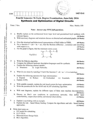
c. For the graph in figure, find the minimum vertex cover.
D Expand ii) Reduce
Explain ATPG.
iii) Irredundant iv) Essentials.
With suitable example, explain the rule based system for logic optimization.
Write the pseudocode for the ASAP and ALAP scheduling algoiltt *.
Note: Answer any FIVE.fall questions"
Briefly explain on the architectural level, logic level and geometrical level synthesis with
relevant figures. (10 Marks)
With necessary diagrams and notations discuss on directed and undirected graphs. (10 Marks)
Give the structural and behavioural representation of Half Adder in rfUOt. (05 Marks)
For a function f : (ab + bc + ac), find the Boolean difference , consensus and smoothing
3a.
b.
c.
4a.
b.
Fig.Q2(c)
Write the Drjkstra algorithm.
Compare the different hardware description languages used for synthesis.
Explain the following abstract models :
D Structures ii) Logic Networks.
What do you mean by tautology? Find if the function f : ab * ac * a'is a tautology.
Explain the following operators for logic minimization ,
t08 Marks)
c.
a.
b.
a.
b.
With neat diagrams, explain the different types of finite state machine decompositions.
(08 Nlarks)
Discuss on Don't care conditions in synchronous networks. Also define input
controllability, output observability and internal observability. (12 Marks)
a. Explain Loop folding with an example.
b. Explain the rule - based library binding. Compare
approaches.
Write short notes on :
a. ILP model for scheduling.
b. LUT FPGA.
c. Microelectronic Design Style.
d. Hu's Algorithm. (20 Marks)

4th Semester M Tech: VLSI Design and Embedded System (June-2016) Question Papers

  • 1.
    th^ U burn fvliTccLtr 14EVE42l 2Arc USN Fourth Time: 3 hrs. o Q Q i< E a E0.) () i- 8R -o uo ll ioo .= c(Bw Y/ cr o.l=eC) d'- -.4) (J"; - '.= i^cs oO bo= 'ob >r.csad- IC(s r? o) 'E ,- or=ad ia. E_ tro- orv ?., -v 6: otE -()=e too ()= =9r =cJvL () U< * C'.1 0) zP 63 1n La. b. c. 2a. b. c. 3a. b. Max. Marks:100 Note: Answer $rry FIVE full questions. Explain CMOS inverter using transfer characteristic and describe aspect ratio with relevant expression. (10 N1arks) Using switch logic, write CMOS NAND gate and CMOS NOR gate diagram. (06 Marks) Compare CMOS and BiCMOS technologies. (04 Marks) Explain MESFET under bias of Vo below pinch off and bias at pinch off with its current - vo ltage characteristic. (10 Marks) Derive an expression for the pinch-ofTvoltage in MESFET with an active layer thickness of Describe the MIS system under three different biased conditions (i.e accumulation, depletion and inversion region). (12 Marks) Calculate the threshold voltage (Vr) for a n-channel MIS device given the following Na : l0l7 cm'', Q, : 10" alcm2, d: 20nm and Q*, : -0.95 V. (08 Marks) With a neat diagram, explain two dimensional potential profile for a long channel MOSFET 't' . Differentiate between MESFE,T arrd MODFET. device and short channel MOSFET device. Describe the processing challenges to further CMOS miniaturization. Explain the differerlces betwccn bulk MOSFET and SOI MOSFET depletion region. Discuss : i) Conventional Vs tactile computation ii) Molecular and biologicai computing. (06 Marks) (04 Marks) (12 Marks) (08 Marks) in the gate controlled (10 Marks) a. b. a. b. a. Explain RC delay line using long silicon trine using suitable rnathematrcal analysis. b. What are super buffers? Explain inverting and non inverting nMOS super butfers. a. Describe 4 input taliy circuits. b. Realize (AB + CD) : y rn i) NN,'IOS ii) CMOS technology, using static AOI. c. Write a note on nMOS multiplxers. Discuss : a. Regularity b. Modularity c. Locality d. Standard ceil e. Full custom design. (10 Marks) (10 Marks) (10 Marks) (10 Marks) (05 Marks) (05 Marks) ****{< (20 Marks)
  • 2.
    USN Fourth Semesten Synthesis Time: 3hrs. 14EVE41 (10 Marks) (05 Marks) (06 Marks) (08 Marks) (06 Marks) (08 Marks) (04 Marks) (10 Marks) (10 Marks) (08 Marks) the algorithmic and rule - based binding (12 Marks) M.Tech. Degree Examination, June/July 2016 and Optimization of Digital Gircuits Max. Marks:100 0) .9 o c0 ! (€ a c) C) ! 8R -}4' 6e 7(.) .^II ccc .= c cd i+ bi0 otrd ,:) frZ a= o4) (do o0( c0(i o a(g 5lrad c.Ltra. 5Cd(); av a)= 5(.) r, tr= t6) 6.Y> q- ooo cc0 (I)= =d:i'I =G)o c< *N c) Z (6: t- C4 E a. b. a. b. with respect to a. c. For the graph in figure, find the minimum vertex cover. D Expand ii) Reduce Explain ATPG. iii) Irredundant iv) Essentials. With suitable example, explain the rule based system for logic optimization. Write the pseudocode for the ASAP and ALAP scheduling algoiltt *. Note: Answer any FIVE.fall questions" Briefly explain on the architectural level, logic level and geometrical level synthesis with relevant figures. (10 Marks) With necessary diagrams and notations discuss on directed and undirected graphs. (10 Marks) Give the structural and behavioural representation of Half Adder in rfUOt. (05 Marks) For a function f : (ab + bc + ac), find the Boolean difference , consensus and smoothing 3a. b. c. 4a. b. Fig.Q2(c) Write the Drjkstra algorithm. Compare the different hardware description languages used for synthesis. Explain the following abstract models : D Structures ii) Logic Networks. What do you mean by tautology? Find if the function f : ab * ac * a'is a tautology. Explain the following operators for logic minimization , t08 Marks) c. a. b. a. b. With neat diagrams, explain the different types of finite state machine decompositions. (08 Nlarks) Discuss on Don't care conditions in synchronous networks. Also define input controllability, output observability and internal observability. (12 Marks) a. Explain Loop folding with an example. b. Explain the rule - based library binding. Compare approaches. Write short notes on : a. ILP model for scheduling. b. LUT FPGA. c. Microelectronic Design Style. d. Hu's Algorithm. (20 Marks)