1. University of Dar es Salaam
Switching Electronics
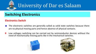
Electronics Switch
The electronic switches are generally called as solid state switches because there
are no physical moving parts and hence absence of physical contacts.
Low voltages switching can be carried out by semiconductor devices without the
need of mechanically moving parts like in the mechanical switches.
2. University of Dar es Salaam
Switching Electronics
Construction-Connection Establishment
Electronic switches do not require any physical contact in order to control a circuit.
These are activated by semiconductor action.
Electronic switches are also referred to as contactless or non-contacting switches.
Electronic switches are electrically operated switches using semiconductor
devices.
Electronics Switch
3. University of Dar es Salaam
Switching Electronics
Electronics Switch
Transistor Switches
BJT
MOSFET
IGBT
IEGT
Thyristor Switches
SCR
GTO
IGCT
4. University of Dar es Salaam
Switching Electronics
Transistor Switch
BJT – Bipolar Junction Transistor
A Bipolar Junction Transistor (BJT) is current controlled device.
A transistor can allow the current to pass or it blocks the current as similar to
working of normal switch.
It offers an open-circuit (𝑅∞) when it is put in the OFF position and a short circuit
(𝑅 = 0) when put in ON position.
A transistor only switches DC output ON or OFF.
5. University of Dar es Salaam
Switching Electronics
Transistor Switch
BJT – Bipolar Junction Transistor
By controlling 𝐼𝐵𝐸, the 𝑅𝐶𝐸 resistance can be either nearly infinity or nearly zero.
6. University of Dar es Salaam
Switching Electronics
Transistor Switch
BJT – Bipolar Junction Transistor
Transistor IV Characteristic Curves.
7. University of Dar es Salaam
Switching Electronics
Transistor Switch
BJT – Bipolar Junction Transistor
A transistor can be made to operate as switch by biasing the base terminal to
operate in the cut-off and saturation regions.
In switching circuits, transistor operates in cut-off mode for OFF or current blocking
condition and in saturation mode for ON condition.
The active region of the transistor is not used for switching applications.
The power loss in these two regional is low but not zero.
The power loss in the active region is large hence avoided in switching operations
to minimize power loss.
8. University of Dar es Salaam
Switching Electronics
BJT – Bipolar Junction Transistor
Cut-Off Region Characteristics
The input and Base are grounded ( 0 V )
Base-Emitter voltage 𝑉𝐵𝐸 < 0.7 V
Base-Emitter junction is reverse biased
Base-Collector junction is reverse biased
Transistor is "fully-OFF" ( Cut-Off region )
No Collector current flows (𝐼𝐶 = 0)
𝑉𝑂𝑈𝑇 = 𝑉𝐶𝐸 = 𝑉𝐶𝐶 ="1"
Transistor operates as an "open switch".
9. University of Dar es Salaam
Switching Electronics
BJT – Bipolar Junction Transistor
Saturation Region Characteristics
The input and Base are connected to 𝑉𝐶𝐶
Base-Emitter voltage 𝑉𝐵𝐸 > 0.7 V
Base-Emitter junction is forward biased
Base-Collector junction is forward biased
Transistor is "fully-ON" ( saturation region )
Maximum collector current flows (𝐼𝐶 =
𝑉𝐶𝐶
𝑅𝐿
)
𝑉𝐶𝐸 = 0 (ideal saturation)
𝑉𝑂𝑈𝑇 = 𝑉𝐶𝐸 = "0"
Transistor operates as a "closed switch"
10. University of Dar es Salaam
Switching Electronics
BJT – Bipolar Junction Transistor
In Practice
In OFF state there is a small leakage current flowing through the transistor ⟹
𝐼𝐶 ≠ 0
In ON state the transistor has a low resistance value causing a small 𝑉𝐶𝐸(𝑠𝑎𝑡) across
it ⟹ 𝑉𝐶𝐸 ≠ 0
Therefore, transistor is not a perfect switch.
11. University of Dar es Salaam
Switching Electronics
BJT – Bipolar Junction Transistor
Power Issues
At both ON and OFF states power dissipation is at its minimum
For 𝐼𝐵 to flow the base terminal must be made more positive than the emitter by
increasing it above 0.7 V.
By varying the base-emitter voltage (𝑉𝐵𝐸), the base current (𝐼𝐵) is also altered and
which in turn control collector current (𝐼𝐶) flow through the transistor.
12. University of Dar es Salaam
Switching Electronics
BJT – Bipolar Junction Transistor
Power Issues
From the figure, when 𝐼𝐵 = 0, 𝐼𝐶 has very
small constant values for wide range of 𝑉𝐶𝐸.
This implies that when a transistor is
operated with 𝐼𝐵 ≤ 0 the 𝐼𝐶 ≅ 0 - is very
tiny.
The power loss across the transistor switch
(𝐼𝐶 × 𝑉𝐶𝐸) is negligible because 𝐼𝐶 is tiny.
13. University of Dar es Salaam
Switching Electronics
BJT – Bipolar Junction Transistor
Power Issues
From the figure 𝐼𝐶 = 𝐼𝐶1 and 𝐼𝐶 < 𝐼𝐶1.
This implies that the transistor is operated in
the saturation region.
Thus, for any 𝐼𝐶 < 𝐼𝐶1 there will be a tiny
𝑉𝐶𝐸.
The current through the transistor will be as
high as the load current.
The power loss is also negligible(𝐼𝐶 × 𝑉𝐶𝐸) is
negligible because 𝐼𝐶 is tiny.
Let 𝐼𝐵 = 𝐼𝐵3
14. University of Dar es Salaam
Switching Electronics
BJT – Bipolar Junction Transistor
Max Power Loss
Maximum power loss happens in a transistor during the transition period of
changing state.
The amount of energy dissipated is quite moderate as the period of transition is
quite small.
For low-frequency operation, the generated heat may be moderated.
But if the frequency of operation is quite high, there will be significant power loss
and corresponding generation of heat.
)
𝑃𝐴𝑉 = 𝜓 𝐼𝑂𝑁 × 𝑉𝑂𝑁 + 𝑓(𝑊𝑂𝑁 + 𝑊𝑂𝐹𝐹
15. University of Dar es Salaam
Switching Electronics
BJT – Bipolar Junction Transistor
Performance
PARAMETER ADVANTAGE DISADVANTAGE
Power handling Small power only
DC switching Capable
AC Switching Not capable
Switching speed Relatively fast
Power loss Relatively small
Contact wear No tear and wear
16. University of Dar es Salaam
Switching Electronics
BJT – Bipolar Junction Transistor
Current Handling Capacity Boosting
Transistor pairing
Darlington Transistor
Boost current 𝐼𝐶
𝛽 = 𝛽1𝛽2
This configuration double voltage drop relative to
single transistor application.
17. University of Dar es Salaam
Switching Electronics
BJT – Bipolar Junction Transistor
Current Handling Capacity Boosting
Transistor pairing
Darlington Transistor – Sziklai configuration
Boost current 𝐼𝐶
𝛽 = 𝛽1𝛽2
This configuration minimizes losses due to
voltage drop.
18. University of Dar es Salaam
Switching Electronics
BJT – Bipolar Junction Transistor
Current Handling Capacity Boosting
Using electromagnetic relay
20. University of Dar es Salaam
Switching Electronics
S.No BJT MOSFET
1 It is a Bipolar Device It is majority carrier Device
2 Current control Device Voltage control Device.
3 Output is controlled by controlling base current Output is controlled by controlling gate voltage
4 Negative temperature coefficient Positive temperature coefficient
5 So, paralleling of BJT is difficult. So, paralleling of this device is easy.
6
Dive circuit is complex. It should provide
constant current(Base current)
Dive circuit is simple. It should provide constant
voltage(gate voltage)
7 Losses are low. Losses are higher than BJTs.
8 So used in high power applications. Used in low power applications.
9 BJTs have high voltage and current ratings. They have less voltage and current ratings.
10 Switching frequency is lower than MOSFET. Switching frequency is high.
22. University of Dar es Salaam
Switching Electronics
Transistor Switch
Device Characteristic Power Bipolar Power MOSFET IGBT
Voltage Rating High <1kV High <1kV Very High >1kV
Current Rating High <500A Low <200A High >500A
Input Drive Current, hFE 20-200 Voltage, VGS 3-10V Voltage, VGE4-8V
Input Impedance Low High High
Output Impedance Low Medium Low
Switching Speed Slow (uS) Fast (nS) Medium
Cost Low Medium High
25. University of Dar es Salaam
Switching Electronics
Electronics Switch
26. University of Dar es Salaam
Switching Electronics
Electronics Switch
Editor's Notes
Image comparisons between the solid-state and electromagnetic relays
BJT – Bipolar Junction Transistor
IEGT (Injection Enhanced Gate Transistor) is a high power device that can control large current with voltage drive which improves the sharp increase of the on-state voltage accompanying the increase in collector-emitter voltage by devising the element structure of the emitter of the IGBT.
NPN transistor
𝑃= 𝐼 𝐶 × 𝑉 𝐶𝐸
𝐼 𝐵 =0 ⟹ 𝐼 𝐶 =0
𝑉 𝐶𝐸 is maximum ⟹ 𝑉 𝐶𝐸 = 𝑉 𝐶𝐶
No current flow through the transistor
The transistor is fully switched OFF.
During switch ON period, the current ( 𝐼 𝐶 ) will be building up while the collector-emitter voltage 𝑉 𝐶𝐸 will be falling towards zero. As the current increases from zero (ideal) to its maximum value and voltage falls from the maximum value to zero (ideal) there will be an instant where both of them will be maximum. At that point, peak power loss happens. In the same way, maximum power loss happens in a transistor when it comes at OFF state from ON state.
BJT Vs Electromagnetic Relay
BJT Vs Electromagnetic Relay
Explain how this reduces voltage drop
BJT Vs Electromagnetic Relay
Did not cover this because of limited knowledge of students on this. Not much is taught at A level Physics