Equipo de sonido lg lm u5050 u4050 a
•
0 likes•637 views

This document is a service manual for various LM-U and LMS-U series 3CD changer hi-fi systems. It contains information for servicing the units, including safety precautions, specifications for the models covered, an electrical troubleshooting guide, internal block diagrams of ICs, schematic diagrams, wiring diagrams, printed circuit board diagrams, and exploded views of components. The manual provides technicians with the information needed to diagnose and repair electrical and mechanical issues with the hi-fi systems.
![- 1-1 -
[CONTENTS]
❍ SECTION 1. GENERAL
• SERVICING PRECAUTIONS . . . . . . . . . . . . . . . . . . . . . . . . . . . . . . . . . . . . . . . . . . . . . . . 1-2
• ESD PRECAUTIONS . . . . . . . . . . . . . . . . . . . . . . . . . . . . . . . . . . . . . . . . . . . . . . . . . . . . . 1-4
• SPECIFICATION . . . . . . . . . . . . . . . . . . . . . . . . . . . . . . . . . . . . . . . . . . . . . . . . . . . . . . . . . .1-5
❍ SECTION 2. ELECTRICAL SECTION
• ELECTRICAL TROUBLESHOOTING GUIDE . . . . . . . . . . . . . . . . . . . . . . . . . . . . . . . . . . . 2-1
• INTERNAL BLOCK DIAGRAM of ICs . . . . . . . . . . . . . . . . . . . . . . . . . . . . . . . . . . . . . . . . . 2-10
• BLOCK DIAGRAM . . . . . . . . . . . . . . . . . . . . . . . . . . . . . . . . . . . . . . . . . . . . . . . . . . . . . . 2-15
• SCHEMATIC DIAGRAMS . . . . . . . . . . . . . . . . . . . . . . . . . . . . . . . . . . . . . . . . . . . . . . . . . 2-19
• WIREING DIAGRAM . . . . . . . . . . . . . . . . . . . . . . . . . . . . . . . . . . . . . . . . . . . . . . . . . . . . . 2-43
• PRINTED CIRCUIT DIAGRAMS . . . . . . . . . . . . . . . . . . . . . . . . . . . . . . . . . . . . . . . . . . . . 2-45
❍ SECTION 3. EXPLODED VIEWS
• CABINET AND MAIN FRAME SECTION . . . . . . . . . . . . . . . . . . . . . . . . . . . . . . . . . . . . . . . .3-1
• TAPE DECK MECHANISM (A/R & A/S : RIGHT A/R DECK) . . . . . . . . . . . . . . . . . . . . . . . . . .3-3
• TAPE DECK MECHANISM (A/R & A/S : LEFT A/S DECK) . . . . . . . . . . . . . . . . . . . . . . . . . . .3-5
• CD MECHANISM . . . . . . . . . . . . . . . . . . . . . . . . . . . . . . . . . . . . . . . . . . . . . . . . . . . . . . . . . 3-7
❍ SECTION 4. SPEAKER PART
• SPEAKER PART . . . . . . . . . . . . . . . . . . . . . . . . . . . . . . . . . . . . . . . . . . . . . . . . . . . . . . . . . .4-1
❍ SECTION 5. REPLACEMENT PARTS LIST
• REPLACEMENT PARTS LIST . . . . . . . . . . . . . . . . . . . . . . . . . . . . . . . . . . . . . . . . . . . . . . . .5-1](data:image/gif;base64,R0lGODlhAQABAIAAAAAAAP///yH5BAEAAAAALAAAAAABAAEAAAIBRAA7)
Recommended
More Related Content
Similar to Equipo de sonido lg lm u5050 u4050 a
Similar to Equipo de sonido lg lm u5050 u4050 a (20)
Recently uploaded
Recently uploaded (20)
Equipo de sonido lg lm u5050 u4050 a
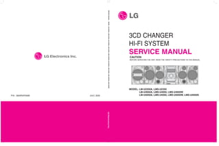
- 1. 3CD CHANGER HI-FI SYSTEM SERVICE MANUAL P/N : 3829RAP006B JULY, 2005 MODEL: LM-U2350A, LMS-U2350 LM-U4050A, LMS-U4050, LMS-U4050W LM-U5050A, LMS-U5050, LMS-U5050W, LMS-U5050S SERVICE MANUAL MODEL: LM-U2350A, LMS-U2350, LM-U4050A, LMS-U4050, LMS-U4050W, LM-U5050A, LMS-U5050, LMS-U5050W, LMS-U5050S CAUTION BEFORE SERVICING THE UNIT, READ THE “SAFETY PRECAUTIONS” IN THIS MANUAL.
- 2. - 1-1 - [CONTENTS] ❍ SECTION 1. GENERAL • SERVICING PRECAUTIONS . . . . . . . . . . . . . . . . . . . . . . . . . . . . . . . . . . . . . . . . . . . . . . . 1-2 • ESD PRECAUTIONS . . . . . . . . . . . . . . . . . . . . . . . . . . . . . . . . . . . . . . . . . . . . . . . . . . . . . 1-4 • SPECIFICATION . . . . . . . . . . . . . . . . . . . . . . . . . . . . . . . . . . . . . . . . . . . . . . . . . . . . . . . . . .1-5 ❍ SECTION 2. ELECTRICAL SECTION • ELECTRICAL TROUBLESHOOTING GUIDE . . . . . . . . . . . . . . . . . . . . . . . . . . . . . . . . . . . 2-1 • INTERNAL BLOCK DIAGRAM of ICs . . . . . . . . . . . . . . . . . . . . . . . . . . . . . . . . . . . . . . . . . 2-10 • BLOCK DIAGRAM . . . . . . . . . . . . . . . . . . . . . . . . . . . . . . . . . . . . . . . . . . . . . . . . . . . . . . 2-15 • SCHEMATIC DIAGRAMS . . . . . . . . . . . . . . . . . . . . . . . . . . . . . . . . . . . . . . . . . . . . . . . . . 2-19 • WIREING DIAGRAM . . . . . . . . . . . . . . . . . . . . . . . . . . . . . . . . . . . . . . . . . . . . . . . . . . . . . 2-43 • PRINTED CIRCUIT DIAGRAMS . . . . . . . . . . . . . . . . . . . . . . . . . . . . . . . . . . . . . . . . . . . . 2-45 ❍ SECTION 3. EXPLODED VIEWS • CABINET AND MAIN FRAME SECTION . . . . . . . . . . . . . . . . . . . . . . . . . . . . . . . . . . . . . . . .3-1 • TAPE DECK MECHANISM (A/R & A/S : RIGHT A/R DECK) . . . . . . . . . . . . . . . . . . . . . . . . . .3-3 • TAPE DECK MECHANISM (A/R & A/S : LEFT A/S DECK) . . . . . . . . . . . . . . . . . . . . . . . . . . .3-5 • CD MECHANISM . . . . . . . . . . . . . . . . . . . . . . . . . . . . . . . . . . . . . . . . . . . . . . . . . . . . . . . . . 3-7 ❍ SECTION 4. SPEAKER PART • SPEAKER PART . . . . . . . . . . . . . . . . . . . . . . . . . . . . . . . . . . . . . . . . . . . . . . . . . . . . . . . . . .4-1 ❍ SECTION 5. REPLACEMENT PARTS LIST • REPLACEMENT PARTS LIST . . . . . . . . . . . . . . . . . . . . . . . . . . . . . . . . . . . . . . . . . . . . . . . .5-1
- 3. - 1-2 - SECTION 1. GENERAL ❏ SERVICING PRECAUTIONS ■ NOTES REGARDING HANDLING OF THE PICK-UP 1. Notes for transport and storage 1) The pick-up should always be left in its conductive bag until immediately prior to use. 2) The pick-up should never be subjected to external pressure or impact. 2. Repair notes 1) The pick-up incorporates a strong magnet, and so should never be brought close to magnetic materials. 2) The pick-up should always be handled correctly and carefully, taking care to avoid external pressure and impact. If it is subjected to strong pressure or impact, the result may be an operational malfunction and/or damage to the printed-circuit board. 3) Each and every pick-up is already individually adjusted to a high degree of precision, and for that reason the adjustment point and installation screws should absolutely never be touched. 4) Laser beams may damage the eyes! Absolutely never permit laser beams to enter the eyes! Also NEVER switch ON the power to the laser output part (lens, etc.) of the pick-up if it is damaged. 5) Cleaning the lens surface If there is dust on the lens surface, the dust should be cleaned away by using an air bush (such as used for camera lens). The lens is held by a delicate spring. When cleaning the lens surface, therefore, a cotton swab should be used, taking care not to distort this. 6) Never attempt to disassemble the pick-up. Spring by excess pressure. If the lens is extremely dirty, apply isopropyl alcohol to the cotton swab. (Do not use any other liquid cleaners, because they will damage the lens.) Take care not to use too much of this alcohol on the swab, and do not allow the alcohol to get inside the pick-up. Storage in conductive bag Drop impact NEVER look directly at the laser beam, and don’t let contact fingers or other exposed skin. Magnet How to hold the pick-up Conductive Sheet Cotton swab Pressure Pressure
- 4. - 1-3 - ■ NOTES REGARDING COMPACT DISC PLAYER REPAIRS 1. Preparations 1) Compact disc players incorporate a great many ICs as well as the pick-up (laser diode). These components are sensitive to, and easily affected by, static electricity. If such static electricity is high voltage, components can be damaged, and for that reason components should be handled with care. 2) The pick-up is composed of many optical components and other high-precision components. Care must be taken, therefore, to avoid repair or storage where the temperature of humidity is high, where strong magnet- ism is present, or where there is excessive dust. 2. Notes for repair 1) Before replacing a component part, first disconnect the power supply lead wire from the unit 2) All equipment, measuring instruments and tools must be grounded. 3) The workbench should be covered with a conductive sheet and grounded. When removing the laser pick-up from its conductive bag, do not place the pick-up on the bag. (This is because there is the possibility of damage by static electricity.) 4) To prevent AC leakage, the metal part of the soldering iron should be grounded. 5) Workers should be grounded by an armband (1M Ω) 6) Care should be taken not to permit the laser pick-up to come in contact with clothing, in order to prevent sta- tic electricity changes in the clothing to escape from the armband. 7) The laser beam from the pick-up should NEVER be directly facing the eyes or bare skin. CLEARING MALFUNCTION You can reset your unit to initial status if malfunction occur(button malfunction, display, etc.). Using a pointed good conductor(such as driver), simply short the RESET jump wire on the inside of the volume knob for more than 3 seconds. If you reset your unit, you must reenter all its settings(stations, clock, timer) NOTE: 1. To operate the RESET jump wire, pull the volume rotary knob and release it. 2. If you wish to operate the RESET jump wire, it is necessary to unplug the power cord. Resistor (1 Mohm) Conductive Sheet Resistor (1 Mohm) Armband RESET jump wire VOLUME VOLUME KNOB DOWN UP
- 5. - 1-4 - ❏ ESD PRECAUTIONS ■ Electrostatically Sensitive Devices (ESD) Some semiconductor (solid state) devices can be damaged easily by static electricity. Such components commonly are called Electrostatically Sensitive Devices (ESD). Examples of typical ESD devices are integrated circuits and some field-effect transistors and semiconductor chip components. The following techniques should be used to help reduce the incidence of component damage caused by static electricity. 1. Immediately before handling any semiconductor component or semiconductor-equipped assembly, drain off any electrostatic charge on your body by touching a known earth ground. Alternatively, obtain and wear a commercially available discharging wrist strap device, which should be removed for potential shock reasons prior to applying power to the unit under test. 2. After removing an electrical assembly equipped with ESD devices, place the assembly on a conductive sur- face such as aluminum foil, to prevent electrostatic charge buildup or exposure of the assembly. 3. Use only a grounded-tip soldering iron to solder or unsolder ESD devices. 4. Use only an anti-static solder removal device. Some solder removal devices not classified as "anti-static" can generate electrical charges sufficient to damage ESD devices. 5. Do not use freon-propelled chemicals. These can generate electrical charges sufficient to damage ESD devices. 6. Do not remove a replacement ESD device from its protective package until immediately before you are ready to install it. (Most replacement ESD devices are packaged with leads electrically shorted together by conductive foam, aluminum foil or comparable conductive materials). 7. Immediately before removing the protective material from the leads of a replacement ESD device, touch the protective material to the chassis or circuit assembly into which the device will by installed. CAUTION : BE SURE NO POWER IS APPLIED TO THE CHASSIS OR CIRCUIT, AND OBSERVE ALL OTHER SAFETY PRECAUTIONS. 8. Minimize bodily motions when handing unpackaged replacement ESD devices. (Otherwise harmless motion such as the brushing together of your clothes fabric or the lifting of your foot from a carpeted floor can gen- erate static electricity sufficient to damage an ESD device). CAUTION. GRAPHIC SYMBOLS THE LIGHTNING FLASH WITH APROWHEAD SYMBOL. WITHIN AN EQUILATERAL TRIANGLE, IS INTENDED TO ALERT THE SERVICE PERSONNEL TO THE PRESENCE OF UNINSULATED “DAN- GEROUS VOLTAGE” THAT MAY BE OF SUFFICIENT MAGNITUDE TO CONSTITUTE A RISK OF ELECTRIC SHOCK. THE EXCLAMATION POINT WITHIN AN EQUILATERAL TRIANGLE IS INTENDED TO ALERT THE SERVICE PERSONNEL TO THE PRESENCE OF IMPORTANT SAFETY INFORMATION IN SERVICE LITERATURE.
- 6. - 1-5 - ❏ SPECIFICATIONS [General] [CD] [Tuner] AM FM (MW) [Speakers] [Subwoofer] [TAPE] Power supply Refer to the back panel of the unit. Power consumption 200 W 110 W Weight 8.5 kg External dimensions (W x H x D) 280 x 370 x 400 mm Frequency response 40 - 18000 Hz Signal-to-noise ratio 75 dB Dynamic range 70 dB Tuning Range 87.5 - 108.0 MHz or 65 - 74 MHz, 87.5 - 108.0 MHz Intermediate Frequency 10.7 MHz Signal to Noise Ratio 60/55 dB Frequency Response 60 - 10000 Hz Tuning Range 522 - 1620 kHz or 520 - 1720 kHz Intermediate Frequency 450 kHz Signal to Noise Ratio 30 dB Frequency Response 120 - 2000 Hz Output Power Front : 270 W + 270 W (LM-U5050 model only) 250 W + 250 W (LM-U4050/U2350 model only) Surround : 110 W + 110 W (LM-U5050 model only) Subwoofer : 350 W (LM-U5050/U4050 model only) T.H.D 0.7% Frequency Response 42 - 20000 Hz Signal-to-noise ratio 80 dB Tape Speed 3000 ± 3 % (MTT-111. NORMAL-SPEED) Wow Flutter 0.25 % (MTT -111, JIS-WTD) F.F/REW Time 120 sec (C-60) Frequency Response 125 - 8000 Hz Signal to Noise Ratio 40 dB Channel Separation 50 dB (P/B)/45 dB (R/P) Erase Ratio 55dB (MTT-5511) Type Bass Reflex 3Way 3 Speaker Bass Reflex 2Way 2Speaker Impedance 6Ω 24Ω Frequency Response 55 - 20000 Hz 60 - 20000 Hz Sound Pressure Level 86 dB/W (1m) 86 dB/W (1m) Rated Input Power 270 W 250 W 110 W Max. Input Power 540 W 500 W 220 W Net Dimensions (W x H x D) 250 X 300 X 415 mm 187 X 258 X 415 mm Weight 9.3 kg 4.3 kg Speaker Name Subwoofer (LMS-U5050W/U4050W) Type 1 Way 1 Speaker Impedance 6Ω Frequency Response 45 - 15000 Hz Sound Pressure Level 84 dB/W (1m) Rated Input Power 350 W Max. Input Power 700 W Net Dimensions (W x H x D) 279 X 320 X 415 mm Weight 10.0 kg LM-U5050 MODEL SECTION LM-U4050 LM-U2350 [Amp] Front speaker (L/R) LMS-U5050 LMS-U4050/U2350 Surround speaker (L/R) [LMS-U5050S] Speaker Name
- 7. - 1-6 -
- 8. - 2-1 - SECTION 2. ELECTRICAL ❏ ELECTRICAL TROUBLESHOOTING GUIDE ■ SMPS POWER CIRCUIT P-SENS PART VKK CHECK SMPS ASSY CN902 ➞ 7PIN 5.1V CHECK MAIN PCB CN710 7PIN 5.1V CHECK MAIN PCB CN304 5PIN 5.1VCHECK FRONT PN302 36PIN 5.1VCHECK FRONT IC306(RESET IC) STATE CHECK U-COM IC304 26PIN 5VCHECK SMPS TROUBLESHOOTING CONSULT CN710 CONNECTION STATE CHECK MAIN PCB PATTERN CUTTING AND SHORT CHECK IC306 INPUTVOLTAGE4V, OUTPUTVOLTAGE.2.1VSTATECHECK IC306 KIA7042 CHANGE NO NO NO YES YES YES YES YES CN710 10PIN DC -33V CHECK IC304 51PIN VOLTAGE CHECK SMPS TROUBLESHOOTING CONSULT NO YES
- 9. - 2-2 - MICOM (IC301) CHECK P-CTRL CHECK "P-SENS" CHECK "RESET" IC304 11 PIN CHECK (HIGH ➞ LOW ➞ HIGH) X301 VIBRATION SIGNAL CHECK IC301 CHANGE PN302 33 PIN "P-CTRL" CHECK (HIGH) CN710 5 PIN CHECK SMPS TROUBLESHOOTING CONSULT IC304 VDD(17,46,72,90) PIN VOLTAGE CHECK P-SENS TROUBLESHOOTING CONSULT Q303 STATE CHECK TR "Q303" CHANGE SMPS TROUBLESHOOTING CONSULT MICOM IC304 STATE CHECK SMPS + MAIN BORD-TO-BORD CHECK MAIN CN710 6 PIN CHECK PN302 35 PIN +5.6V(MI) CHECK X301 CHANGE NO NO NO NO YES YES YES YES NO NO YES YES
- 10. - 2-3 - MUTING TROUBLESHOOTING (MUTE STATE) EXPEND IC(IC305/501/502) STATE Q752(A102) BASE "HIGH" Q701, Q751(D1302) BASE "HIGH" CHECK 16 PIN VDD VOLTAGE CHECK 3 "EXP-CLK" CHECK 2 "EXP-DATA" CHECK 4 PIN ~ 15 PIN EACH PORT STATE CHECK EXPEND IC OK MUTE EXPEND IC(IC305) 5PIN HIGH STATE CHECK Q752(A102)STATE CHECK Q752(A102) FAULTY IS CHANGE EACH PART TR CHANGE D332/D553/D551(1SS133) CHECK D332/D553/D551(1SS133) CHANGE PCB PATTERN CHECK PCB PATTERN CHECK MICOM (IC304) 4/84/85 PIN CHECK(CLK1/2/3) MICOM (IC304) 3 PIN CHECK EXPEND IC FAULTY IS CHANGE NO NO NO NO NO NO NO NO NO YES YES YES YES YES YES YES YES YES YES YES YES
- 11. - 2-4 - SPECIFIC FUNCTION MODE HAS NO SOUND (NJW1190) IC601 IC201 INPUT CHECK(HEAD INPUT)"A"DECK 32,39 "B"DECK 34,37 DECK HEAD WIRE CONNECTION STATE CHECK IC502 10PIN(PB MUTE) STATE STATE CHECK IC502 4PIN(REC SW) "LOW" STATE REC Q212 (C) "HIGH" CHECK Q213 (C) "LOW" CHECK IC502 13 PIN "REC-BAIS" HIGH CHECK L203(4.7MH) COIL VIBRATION SIGNAL CHECK IC601 7 /32 INPUT REC' SIGNAL CHECK IC502 4PIN(REC SW) "HIGH" CHECK IC601(NJW1190) TROUBLESHOOTING CONSULT IC502 2 PIN/3 PIN CHECK(DATA/CL IC502 16 PIN VDD CHECK IC502 EXPEND IC CHANGE IC201 OUTPUT CHECK(5,26 PIN) IC601 3,36PIN INPUT SIGNAL CHECK IC601 17,22 PIN OUTPUT SIGNAL CHECK DECK OUTPUT 1) 1) YES YES YES YES YES YES YES YES YES YES YES YES NO NO NO NO NO
- 12. - 2-5 - AUX JK601 SIGNALINPUT CHECK IC601 5,34 PIN SIGNALINPUTCHECK IC601 17,22 PIN OUTPUT SIGNAL CHECK MAIN PCB PATTERN CHECK IC601(NJW1190) TROUBLESHOOTING CONSULT MAIN PCB PATTERN CHECK IC601(NJW1190) TROUBLESHOOTING CONSULT AUX OUTPUT CD CN709 1,3PIN SIGNALCHECK CD TROUBLESHOOTINGCONSULT IC601 4,35PIN SIGNALINPUTCHECK IC601 17,22 PIN OUTPUT SIGNAL CHECK CD OUTPUT YES YES YES YES YES YES YES YES NO NO NO NO
- 13. - 2-6 - TUNER TU101 3 /5 SIGNAL CHECK IC601 2,37 PIN SIGNALINPUTCHECK IC601 17,22 PIN OUTPUT SIGNAL CHECK TU101 2 PIN "+9V" VOLTAGE CHECK TU101 6,7,8,9 PIN CHECK (PLL-CE, PLL-DI, CLK, PLL-DO) TUNER MODULE CHANGE TUNER OUTPUT MIC CN303 7 PIN "MIC-SIGNAL" CHECK IC601 44 PIN SIGNAL CHECK(OW601 PATTERN) IC601 17,22 PIN OUTPUT SIGNAL CHECK CN303 4 MIC-SENSE CHECK PN400 3 PIN "+12V"CHECK TR CHANGE MIC MUTE CHECK(Q409/ Q408) IC402 8 PIN SIGNAL INPUT CHECK PN400 9 "VOL-IN"CHECK IC402 2 PIN SIGNAL INPUT CHECK PN400 10 PIN "VOL-OUT"CHECK MIC OUTPUT <MIC PCB> YES YES YES YES YES YES YES YES YES YES YES YES NO NO NO NO NO
- 14. - 2-7 - IC601(NJW1190) TROUBLESHOOTING IC601 24PIN VOLTAGE INPUT CHECK IC601 19,20 SDA, SCA PULSE WAVE CHECK (VOL UP, DOWN TURN CHECK) IC601 17.22 PIN WAVE OUTPUT CHECK IC601 OK FUNCTION INPUT PORT SIGNAL CHECK(NJW1190 TROUBLESHOOTING) SMPS VOLTAGE CHECK CONSULT IC301 10,8PIN CHECK IC301 TROUBLESHOOTING IC601 CHANGE NO NO NO YES YES YES YES YES YES YES YES YES AMP MODULE TROUBLESHOOTING IC501 9 PIN(AMP-PWR)HIGH CHECK EXPEND IC TROUBLESHOOTING CONSULT PROTECTION " HIGH" ➞ SMPS VOLTAGE AND AMP ON/ OFF STATE CHECK AMP MODULE CHECK : MOS FET BOTH ARE READ SHORT ➞ AMP DEAD AMP MODULE CHANGE IC305 9 PIN(AMP-PWR) HIGH CHECK IC701 11 PIN "AMP-ON/OFF" HIGH CHECK IC701 12 PIN "PROTECTION" LOW CHECK PN702 3 PIN "PROTECTION"CHECK (HIGH ➞ LOW) NO NO NO IC701 3 ,20 & 5 ,18 EACH +65V &-65V CHECK SMPS TROUBLESHOOTING CONSULT YES NO
- 15. - 2-8 - IC701 9 ,14 ±9V CHECK IC701 10 , 13 INPUT SIGNAL CHECK IC701 5 ,17 OUTPUT SIGNAL CHECK OK SMPS TROUBLESHOOTING CONSULT REC INPUTCHECK CHECK INPUT LINE CHECK IC202 4PIN STATECHECK Q205 BASE 0.6V CHECK VOLTAGE CHECK CONSULT IC202TROUBLESHOOTING CHECK Q204 CHANGE L203 CHANGE Q204 COLLECTOR LOW Q203 CHANGE OK REC OUTPUTCHECK AFTER FAULTY IS ICCHANGE YES YES YES YES YES YES YES YES YES YES NO REC CHECK (Q252,Q202 ON :R273,R223 HIGH) IC601 24PIN VOLTAGE INPUT CHECK IC201 7,24 PIN INPUT CHECK IC201 10.21 PIN OUTPUT CHECK L203 2,3PIN CHECK IC202 14 PIN STATESTATE CHECK Q213.212 STATE STATECHECK DECK CHANGE IC401 EACH INPUTTUNER6,39.TAPE. 7.38.CD. 8.38.AUX.9.36 PIN SIGNAL INPUT CHECK NO NO NO NO NO NO NO NO
- 16. - 2-9 - DUBBING CHECK ("NORMAL OR REC"//"HIGH") IC401 11,34 OUTCHECK REC INPUTCHECK CHECK INPUT LINE CHECK IC201 7,24 PIN INPUT CHECK IC201 10.21PIN OUTPUT CHECK IC401 EACH INPUTTUNER6,39.TAPE. 7.38.CD.8.38.AUX.9.36PIN SIGNAL INPUT CHECK YES YES YES NO NO
- 17. - 2-10 - ❏ INTERNAL BLOCK DIAGRAM of ICs • HA12237F BLOCK DIAGRAM
- 18. - 2-11 - • NJW1190 BLOCK DIAGRAM • AF330W20FS BLOCK DIAGRAM
- 19. - 2-12 - PIN CONFIGURATION PIN DESCRIPTION Pin Number Symbol Type Description 1 L_DO O L-Channel Drain Output 2 SUBGND G Sub Ground 3 VDD_L P L-Channel Positive supply Voltage 4 L_GND P L-Channel Signal Ground 5 VSS_L O L-Channel Negative supply Voltage 6 L_OUT G L-Channel Audio Output 7 AM_F1 I AM Mode control Input 1 8 L_CS I L-Channel Current Sense Input 9 VCC P Positive supply Voltage 10 L_IN I L-Channel Audio Input 11 STANDBY I ON/OFF control 12 P_STATE O Protection State 13 R_IN I R-Channel Audio Input 14 VEE P Negative supply Voltage 15 R_CS I R-Channel Current Sense Input 16 AM_F2 I AM Mode control Input 2 17 R_OUT G R-Channel Audio Output 18 VSS_R O R-Channel Negative supply Voltage 19 R_GND P R-Channel Signal Ground 20 VDD_R P R-Channel Positive supply Voltage 21 SUBGND G Sub Ground 22 R_DO O R-Channel Drain Output
- 20. - 2-13 - • AF350W01FS BLOCK DIAGRAM PIN CONFIGURATION
- 21. - 2-14 - PIN DESCRIPTION Pin Number Symbol Type Description 1 N_DO O NMOS Drain Output 2 VSS P Negative supply Voltage 3 N_CS I NMOS Current Sense Input 4 P_CS I PMOS Current Sense Input 5 NC 6 NC 7 VEE P Negative supply Voltage 8 STANDBY I ON/OFF control 9 IN I Audio Input 10 P_STATE O Protection State 11 VCC P Positive supply Voltage 12 OUT O Audio Output 13 GND G Signal Ground 14 SUBGND G Sub Ground 15 VDD P Positive supply Voltage 16 P_DO O PMOS Drain Output
- 22. 2-15 2-16 ❏ BLOCK DIAGRAM
- 23. 2-17 2-18 ❏ WMA_USB BLOCK DIAGRAM
- 24. 2-19 2-20 ❏ SCHEMATIC DIAGRAMS • FRONT SCHEMATIC DIAGRAM
- 25. 2-22 2-21 • MAIN SCHEMATIC DIAGRAM
- 26. 2-23 2-24 • DECK SCHEMATIC DIAGRAM
- 27. 2-26 2-25 • MIC SCHEMATIC DIAGRAM
- 28. 2-27 2-28 • USB_AUX2_H/P SCHEMATIC DIAGRAM
- 29. 2-30 2-29 • WOOFER AMP SCHEMATIC DIAGRAM
- 30. 2-31 2-32 • AMP SCHEMATIC DIAGRAM
- 31. 2-34 2-33 • SUB POWER SCHEMATIC DIAGRAM
- 32. 2-35 2-36 • POWER SCHEMATIC DIAGRAM (LM-U5050/U4050/K9550/D7550)
- 33. 2-37 2-38 • POWER SCHEMATIC DIAGRAM (LM-U2350/K9250/D7250 SERIES)
- 34. 2-39 2-40 • CDP SCHEMATIC DIAGRAM
- 35. 2-41 2-42 • USB SCHEMATIC DIAGRAM
- 36. 2-43 2-44 ❏ WIRING DIAGRAMS
- 37. ❏ PRINTED CIRCUIT DIAGRAMS • MAIN P.C. BOARD 2-45 2-46
- 38. 2-47 2-48 • MAIN AMP P.C. BOARD
- 39. 2-49 2-50 • MAIN AMP P.C. BOARD
- 40. 2-51 2-52 • FRONT P.C. BOARD
- 41. 2-53 2-54 • CDP P.C. BOARD
- 42. 2-55 2-56 • CDP P.C. BOARD
- 43. 2-57 2-58 • POWER P.C. BOARD
- 44. 2-59 2-60 • POWER P.C. BOARD
- 45. 2-61 2-62 • SUB POWER P.C. BOARD
- 46. 2-63 2-64 • WOOFER AMP P.C. BOARD
- 47. 2-65 2-66
- 48. 3-1 3-2 SECTION 3. EXPLODED VIEWS A26 290 279 450 280 450 285 278 A52 281 451 451 282 277 276 A47 453 283 283 301 A46 275 248 A51 A56 A41 452 253 267 287 266 265 450 A54 255 251 258 250 288 303 450 A48 254 A49 256 257 270 272 273 271 A43 450 289 A00 274 269 261 262 263 264 260 268 259 450 252 286 284 302 296 305 *OPTION Caution point A50: Headphone + MIC + USB + Main array assembly pcb. • CABINET AND MAIN FRAME SECTION
- 49. 3-4 3-3 • TAPE DECK MECHANISM (A/R & A/S : RIGHT A/R DECK) 025 504 023 015 022 019 037 021 020 505 018 017 016 506 006 A01 402 008 401 001 002 003 502 507 501 502 402 401 009 401 009 011 013 A02 403 007
- 50. 3-5 3-6 • TAPE DECK MECHANISM (A/R & A/S : LEFT A/R DECK) 016 401 018 007 035 008 015 023 019 021 034 020 505 017 403 504 025 033 502 009 401 003 501 401 011 013 009 022 A03
- 52. - 4-1 - SECTION 4. SPEAKER SECTION ❏ MODEL: LMS-U2350, LMS-U4050, LMS-U5050 WIRE 80 865 851 864 869 866 850 852 868 853 855 854 A80 856 870 851 (LEFT) (RIGHT) 863 862 857 860 (LEFT) 867 859 858 WIRE 81
- 53. - 4-2 - ❏ MODEL: LMS-U5050W, LMS-U4050W 750 WIRE 71 WIRE 72 752 772 783 751 762 A70 A75 760 770 754 756 755 758 757 759 761 753 771
- 54. - 4-3 - ❏ MODEL: LMS-U5050S WIRE 62 WIRE 61 651 650 661 660 659 658 655 663 654 653 A60 662 WIRE 63 665 (RIGHT) (LEFT) 657 656 (RIGHT) (LEFT)
- 55. - 4-4 -