More Related Content
More from Mega Componentes
More from Mega Componentes (20)
000669
- 1. ICs for Audio Common Use
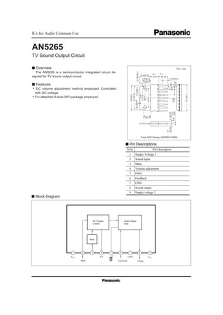
s Overview
The AN5265 is a semiconductor integrated circuit de-
signed for TV sound output circuit.
s Features
• DC volume adjustment method employed. Controlled
with DC voltage.
• Fin-attached 9-lead SIP package employed
AN5265
TV Sound Output Circuit
s Block Diagram
1 2 3 4 5 6 7 8 9
+
Mute
DC Volume
Control
Audio Output
Amp.
Vol GND
OutputFeed backInput
VCC1 VCC2
9
8
7
6
5
4
3
2
1
ø3.3±0.10.1±0.05
5.6±0.25
±0.25
1.7
1.7±0.25
0.45+0.1
–0.05
ø2.65±0.1
8.4±0.25
6.3 7.1
3.75±0.25
0.5
±0.1
1.2
±0.25
2.54
Unit : mm
9-lead HSIP Package (HSIP009-P-0000)
15.0
19.9±0.1
18.3±0.25
5.8±0.25
1.5±0.25
±0.3 ±0.25
22.3±0.3
Supply Voltage 1
Sound Input
Mute
Volume adjustment
Filter
Pin No.
1
2
3
4
5
Pin Description
Feedback
GND
Sound output
Supply voltage 2
6
7
8
9
s Pin Descriptions
- 2. ICs for Audio Common UseAN5265
Parameter Symbol Rating Unit
V1 – 7
V9 – 7
V3 – 7
V4 – 7
V6 – 7
I4
I8
Tstg
Voltage
Current
Storage Temperature – 55 ~ + 150
V
A (peak)
˚C
V
V
V
mA (peak)
26
0
0
14.4
7
V1 – 7
PDPower Dissipation 1.6 W
ToprOperating Ambient Temperature – 20 ~ + 70 ˚C
0
–10
V9 – 7
3
–1.2 1.2
V
Supply Voltage
Circuit Current
Circuit Voltage
s Absolute Maximum Ratings (Ta= 25˚C)
7.1 9.5 11.9 mA
f= 1kHz, V4= 12V, V8= 0Vrms 2.45 2.65 2.85 V
I1
V3 – 7
V2 – 7
V5 – 7
V6 – 7
Circuit Current
Muting Operation Voltage
Circuit Voltage
Circuit Voltage
Circuit Voltage
5.4
8.5
8.8
V
V
V
min.Condition typ. max. UnitSymbol
V8 – 7Circuit Voltage 8.8 V
Pomax.Max. Output Power 2.0 2.3 W
GV f= 1kHz, Vi= 0.1Vrms, V4= 12VVoltage Gain 28.5 30.5 32.5 dB
THD f= 1kHz, PO= 1W,V4= 12VTotal Harmonics Distortion 0.8 1.2 %
Att f= 1kHz, Vi= 0.1Vrms, V4= Ratio between 12 and 0 VMax. Attenuation Amount –95 –85 dB
Vno Vi= 0Vrms, V4= 0VOutput Noise Voltage 0.6 1.0 mVrms
s Electrical Characteristics (Ta= 25˚C)
Pin1= Pin4 = 12V, Pin7= 0V, Pin9 = 18V
Pin1= 12V, Pin4 = Pin7= 0V, Pin9 = 18V
Pin1= 12V, Pin4 = Pin7= 0V, Pin9 = 18V
Pin1= 12V, Pin4 = Pin7= 0V, Pin9 = 18V
Pin1= 12V,Pinr= Pin4= 0V,Pin9=18V,Pin6–8:10kΩ
f= 1kHz, THD= 10%, V4= 12V, RL= 16Ω
Parameter
s Application Circuit
1
2
3
4
5
6
7
8
9
10
11
12
0
PD – Ta
PowerDissipationPD(W)
Ambient Temperature Ta (˚C)
Tc=Ta
Without heat
sink
–20 0 20 40 60 80 100 120 140 160 180
AN5265
+
–
+
–
10kΩ
100µF
VCC=18V
+
–
+
–+
–
+
–
10µF 0.047µF
100µF
100µF
10µF
1µF
4.7Ω
680Ω RL =16Ω
VCC=12V
AF Input Mute
21 3 4 5 6 7 8 9