Designing of Asynchronous Viterbi Decoder for Low Power Consumption using Han...
Dm31762765
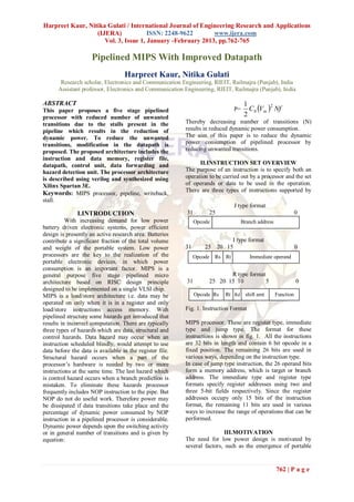
1. Harpreet Kaur, Nitika Gulati / International Journal of Engineering Research and Applications
(IJERA) ISSN: 2248-9622 www.ijera.com
Vol. 3, Issue 1, January -February 2013, pp.762-765
Pipelined MIPS With Improved Datapath
Harpreet Kaur, Nitika Gulati
Research scholar, Electronics and Communication Engineering, RIEIT, Railmajra (Punjab), India
Assistant professor, Electronics and Communication Engineering, RIEIT, Railmajra (Punjab), India
ABSTRACT
C 0 Vin Nf
1 2
This paper proposes a five stage pipelined P=
processor with reduced number of unwanted 2
transitions due to the stalls present in the Thereby decreasing number of transitions (N)
pipeline which results in the reduction of results in reduced dynamic power consumption.
dynamic power. To reduce the unwanted The aim of this paper is to reduce the dynamic
transitions, modification in the datapath is power consumption of pipelined processor by
proposed. The proposed architecture includes the reducing unwanted transitions.
instruction and data memory, register file,
datapath, control unit, data forwarding and II.INSTRUCTION SET OVERVIEW
hazard detection unit. The processor architecture The purpose of an instruction is to specify both an
is described using verilog and synthesized using operation to be carried out by a processor and the set
Xilinx Spartan 3E. of operands or data to be used in the operation.
There are three types of instructions supported by
Keywords: MIPS processor, pipeline, writeback,
stall.
J type format
I.INTRODUCTION 31 25 0
With increasing demand for low power Opcode Branch address
battery driven electronic systems, power efficient
design is presently an active research area. Batteries
contribute a significant fraction of the total volume I type format
and weight of the portable system. Low power 31 25 20 15 0
processors are the key to the realization of the Opcode Rs Rt Immediate operand
portable electronic devices, in which power
consumption is an important factor. MIPS is a
general purpose five stage pipelined micro R type format
architecture based on RISC design principle 31 25 20 15 10 5 0
designed to be implemented on a single VLSI chip.
MIPS is a load/store architecture i.e. data may be Opcode Rs Rt Rd shift amt Function
operated on only when it is in a register and only
load/store instructions access memory. With Fig. 1. Instruction Format
pipelined structure some hazards get introduced that
results in incorrect computation. There are typically MIPS processor. These are register type, immediate
three types of hazards which are data, structural and type and jump type. The format for these
control hazards. Data hazard may occur when an instructions is shown in fig. 1. All the instructions
instruction scheduled blindly, would attempt to use are 32 bits in length and contain 6 bit opcode in a
data before the data is available in the register file. fixed position. The remaining 26 bits are used in
Structural hazard occurs when a part of the various ways, depending on the instruction type.
processor’s hardware is needed by two or more In case of jump type instruction, the 26 operand bits
instructions at the same time. The last hazard which form a memory address, which is target or branch
is control hazard occurs when a branch prediction is address. The immediate type and register type
mistaken. To eliminate these hazards processor formats specify register addresses using two and
frequently includes NOP instruction to the pipe. But three 5-bit fields respectively. Since the register
NOP do not do useful work. Therefore power may addresses occupy only 15 bits of the instruction
be dissipated if data transitions take place and the format, the remaining 11 bits are used in various
percentage of dynamic power consumed by NOP ways to increase the range of operations that can be
instruction in a pipelined processor is considerable. performed.
Dynamic power depends upon the switching activity
or in general number of transitions and is given by III.MOTIVATION
equation: The need for low power design is motivated by
several factors, such as the emergence of portable
762 | P a g e
2. Harpreet Kaur, Nitika Gulati / International Journal of Engineering Research and Applications
(IJERA) ISSN: 2248-9622 www.ijera.com
Vol. 3, Issue 1, January -February 2013, pp.762-765
systems, thermal considerations, reliability issues In the earlier research, the bypassing of memory
and environmental concerns. Low power access stage for arithmetic instructions occurs after a
consumption helps to reduce heat dissipation, store/branch/jump instruction. The store instruction
lengthen battery life, and increase device reliability. has NOP stage during write back stage while
In battery powered applications, where speed is less arithmetic instruction have NOP stage during
of a concern, pipelined processors are often used. memory access stage. Hence write back stage of
The pipeline stages of MIPS for different type of arithmetic instruction can be moved to the memory
instructions are shown in fig. 2. access stage without any resource conflict as shown
in fig. 3. This bypassing of data can be continued till
the load instruction is encountered.
In the scenario if arithmetic instruction appears after
STORE INSTRUCTION load instruction the only possible way to overcome
the conflict was to insert a NOP to the arithmetic
IF ID EX MEM NOP
instruction before its writeback stage. The idea
presented in this paper is to overcome this problem
of inserting NOP instruction, as it leads to delay of
LOAD INSTRUCTION one cycle and the transition of signal leads to power
consumption. This is done by bypassing a memory
IF ID EX MEM WB
access stage even after load instruction is
encountered as shown in fig. 4
clk clk clk clk clk clk
sR TYPE and AIRTHMETIC I TYPE clk1
2 3 4 5 6 7 clk8 clk9
I E N
IF ID EX NOP WB ID MEM
Store F X OP
N W
Arithmetic IF ID EX OP B
BRANCH INSTRUCTION E N
Arithmetic
IF ID X OP WB
IF ID EX MEM NOP E ME
Load
IF ID X M WB
Arithmetic IF ID EX NOP
JUMP INSTRUCTION WB
IF ID NOP NOP NOP Fig. 4. Reconfigured Pipelining with Bypassing
Fig. 2. Pipelined Representation of Instructions IV. PROPOSED ARCHITECTURE
The proposed pipelined architecture of the
It can be seen that arithmetic type instruction do not processor is shown in fig. 5. It includes the
use memory access stage. Store instruction do not instruction and data memory, register file, datapath,
require write-back stage while load instruction go control unit, data forwarding unit and hazard
through all pipeline stages. Transitions during the detection unit
unused stage cause extra power consumption. These
unwanted transitions can be reduced by by-passing Instruction memory: The instruction memory
the unused pipeline stage. In arithmetic instruction contains the instructions that are executed by the
memory access stage is not used, so data obtained processor. It is 32 by 1024 bytes wide and takes 32
from the execution stage is forwarded directly to bit address from the program counter as an input and
write back stage. gives 32 bit instruction word as an output.
clk clk clk clk clk clk
clk1
2 3 4 5 6 7 clk8 clk9 Data memory: Data memory is accessed by the load
I E N and store instructions and it is 32 by 256 bytes wide.
ID MEM
Store F X OP
N W
Register file: Register file contains thirty two 32 bit
Arithmetic IF ID EX OP B
E N
general purpose registers. Generally it has two read
Arithmetic ports and one write port but in this proposed
IF ID X OP WB
E ME architecture register file has two read ports and two
Load write ports and therefore can perform two
IF ID X M WB
Arithmetic IF ID EX NOP WB simultaneous read and write operations.
Fig. 3. Pipelining with Bypassing Datapath: The datapath consist of 5 stage pipelined
structure. The five stages are fetch, decode, execute,
763 | P a g e
3. Harpreet Kaur, Nitika Gulati / International Journal of Engineering Research and Applications
(IJERA) ISSN: 2248-9622 www.ijera.com
Vol. 3, Issue 1, January -February 2013, pp.762-765
memory access and write back stage. Pipeline the data memory and the read or write operation is
registers are placed between each stage and they are performed in accordance with instruction type.
used to carry the result of the previous stage to the
following stages. Write-back stage: During this stage, the results of
the calculation from the execute stage or from the
Fetch stage: In this stage, the content of the program memory access stage are updated into the registers
counter is used to access memory and fetch the next in the register file. The updated value is fetched in
instruction to be executed. accordance with the type of instruction. For
arithmetic instructions the value is taken directly
Decode stage: During this stage, the instruction is from the execute stage, whereas for the load
decoded and the required operands are retrieved and instruction this value is taken from the memory
the opcode is passed to the control unit which access stage.
asserts the required control signals. The idea of
implementation of dual write port is achieved by a Control unit: The control unit is responsible for
signal generated during the instruction decode stage. generating signals that are used for coordinating all
components of entire processor. Moreover the dual
Execute stage: All the instructions fetched through signal which is necessary for dual writeback
the instruction memory are computed in this cycle operation is also generated by the control unit.
and the data generated during this cycle is passed on Data forwarding unit: This unit is responsible for the
to the next pipeline. This cycle includes
Hazard Detection
Control
unit
A Write
Instruction Register L
Data
PC memory file memory back
U
Forwarding Unit
Fig. 5. Proposed MIPS architecture proper flow of data. Forwarding is implemented by
feeding back the output of instruction into the
effective address calculation for load/store previous stage of the pipeline as soon as the output
instructions. Whenever load instruction is of that instruction is available.
encountered a dual signal is asserted high in decode
stage which is responsible to facilitate dual write Hazard Detection unit: This unit detects conditions
back for register type instruction following load under which data forwarding is not possible and
instruction and the write back value is taken directly stalls the pipeline for one or two clock cycles so that
from alu result and are written back to the register instructions can be executed in the correct sequence.
file using second data bus. This second data bus is
powered up only when the dual signal is high. So V.RESULT
execute stage decides whether the data should be After modeling the design of 32 bit MIPS
written back to register file directly from ALU or through verilog, it was synthesized using Xilinx
through writeback stage. Spartan 3E. Power analysis was done using Xpower
estimator. The design had a maximum frequency of
Memory access stage: If the instruction being operation of 193.98Mhz. Fig. 6. shows the results of
executed is of the load or store type, then the data power analysis.
memory is accessed during this stage. The
previously calculated effective address is applied to
764 | P a g e
4. Harpreet Kaur, Nitika Gulati / International Journal of Engineering Research and Applications
(IJERA) ISSN: 2248-9622 www.ijera.com
Vol. 3, Issue 1, January -February 2013, pp.762-765
Power 7 V. Venkatachalam and M.Franz. “Power
Power Power
consumption reduction techniques for microprocessor
consum consumptio
with dual systems,” ACM Computing Surveys,
Clock Toggle ption in n with
writeback(pr September 2005, vol. 37, no. 3, pp. 195-237.
(MHZ) rate normal single write
oposed 8 A. Correale, “ Overview of the power
pipeline back
work) minimization techniques employed in the IBM
(in W) (in W)
(in W) PowerPC 4xx embedded controllers,” in proc.
Of the ACM/IEEE International Symposium on
194 100% 1.359 1.139 1.064
Low Power Design, April 1995, pp. 75-80.
150 75% 1.022 0.857 0.659 9 R. Razdan and M.D. Smith, “A High
Performance Micro architecture with Hardware
100 50% 0.686 0.577 0.340 Programmable Functional Units,” Proc. Micro-
27, IEEE Computer Society ,1994, pp. 172-180.
Fig. 6. Table for Power Consumption Comparison
VI. CONCLUSION
In this work, we proposed a method for
minimizing unnecessary transitions by reducing
stalls in the pipeline. The proposed approach
utilized dual write port register file. The processor
was successfully designed in verilog HDL,
simulated with Modelsim and synthesized on to a
Xilinx Spartan 3E.
REFERENCES
1 D.A.Patterson and J.L.Hennessy, Computer
Organization and Design, The
hardware/software interface. Morgan
Kaufmann, 2005.
2 Gautham P, Parthasarathy R, Karthi
Balasubramanian, “Low Power Pipelined MIPS
Processor Design,” in the proceedings of the
2009 12th international symposium,2009 pp.
462-465.
3 A. A. S. Pejman Lotfi Kamran, Amir
Mohammad Rahmani and A. A. Kusha, “Stall
power reduction in pipelined architecture
processors,” in Proceedings of the 21st
International Conference on VLSI Design,
2008, pp. 541-546.
4 Xia Li, Longwei Ji, Bo Shen, Wenhong Li and
Qianling Zhang, “VLSI Implementation of a
High Performance 32 bit RISC
Microprocessor,” International Conference on
Communications, Circuits and Systems and
West Sino Expositions, IEEE 2002, Vol. 2, pp.
1458-1461.
5 Zhenyu Gu, Zhiyi Yu, Bo Shen and Qianling
Zhang, “Functional Verification Methodolgy of
a 32 bit RISC Processor,” International
Conference on Communications, Circuits and
Systems and West Sino Expositions, IEEE
2002, Vol. 2, pp. 1454-1457.
6 M. S. I. Mamun Bin Ibne Reaz and M. S.
Sulaiman, “A single cycle mips risc processor
design using vhdl,” in Proceedings of IEEE
International Conference on Semiconductor
Electronics, Dec 2002, pp. 199-203.
765 | P a g e