1. MICROPROCESSOR BASED SOLAR TRACKING SYSTEM USING STEPPER MOTOR
Jyotirmay Gadewadikar
B. E. Final Year (Electronics), S.G.S. Institute of Tech. & Science, Indore
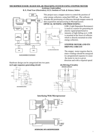
This project uses a stepper motor to control the position of
solar energy collectors, using Intel 8085 mp . The software
includes the positioning of collectors through stepper motor &
data acquisition and processing in Microprocessor.
OPTICAL SENSING AND PROCESSING :
LDR ( Light Dependent Resistance)
+ Vcc
is used as a sensor for generating an
10 K
electric signal proportional to LDR
intensity of light falling on it. LDR
LM
324
is mounted at the focus of reflector
IK
SL 100
which is directly mounted on solar
GND
energy collectors.
R1 = 18
STEPPER MOTOR AND ITS
GND
DRIVING CIRCUIT
L.D.R. SIGNAL PROCESSING CIRCUIT
The stepper motor requires that its
stator windings should be energized
in a programmed sequence to cause
the motor to run in a given
direction and with a required speed.
Hardware design can be categorized into two parts
(a) Logic sequence generating circuit (b) Driving Circuitry
+5V DRIVER CIRCUIT
16 11
LOAD +5V
7
14
CLOCK 4
14
Q 1
A
1 3
3
9 Q 2
2 B
DOWN/UP 1
5
7486
7
ENABLE
4
8 TO GREEN
+5V
14
1 2 TO BLUE
3 4 TO ORANGE
7404
TO RED
LOGIC SEQUENCER CIRCUIT
Interfacing With Microprocessor
Vcc
EXPANDER PORT ONE
B7 B7
A
D TO LDR.
C CIRCUIT
8
B0 D0 0
9
A
B
C0 C
START
ALE
OE
EOC
CLK
C7
GND.
A7
A0
EXPANDER PORT TWO
C7
C1 MODE
GND. CLK.
GND.
TO MOTOR
DRIVER
1
2. THE TRACKING SOFTWARE
MAIN PROGRAM
START
LOAD M WITH 9200 LOCATION FOR
STORING O/P OF ADC. LOAD 9240 WITH 004
INITIALIZE 8255 A AND 8255 B
SELECT ANALOG INPUT CHANNEL ZERO
JUMP TO SUBROUTINE
MAKE OE LINE OF ADC LOW TO
ENABLE OUTPUT LINES
READ DIGITAL O/P AT PORT B OF
8255 B AND STORE IT INTO ACC.
TRANSFER CONTENT OF ACC. INTO
REG. D (NEW VALUE)
LOAD CONTENT OF M INTO ACC.
ACC. CONTAINS PREVIOUS VALUE
YES
LOAD REG H WITH PRESET NO
MIN. DIFFERENCE BETWEEN INCREASE M LOCATION BY ONE
SUCCESSIVE VALUES OF ADC.
SET THE CARRY TO ONE MOVE CONTENTS OF C INTO ACC.
YES YES
END
NO NO
LOAD ACC. WITH THE CONTENT MOVE CONTENT OF REG D
OF LOCATION M INTO ACC.
MOVE CONTENT OF ACC. MOVE CONTENT OF LOCATION M
TO D REG FROM ACC.
GO TO REVERSE MOTOR M : MEMORY LOCATION DENOTED BY
ROTATE REG. PAIR BC
SUBROUTINE FORWARD MOTOR ROTATE REVERSE MOTOR ROTATE
START START START
LOAD THE REG. H WITH OO4
DISABLE THE OUT PUT LOAD THE REG. H WITH 00H MAKE P1C1 LINE OF 8255 A
ENABLE OE OF ADC HIGH FOR COUNT DOWN MODE
MAKE P1C1 LINE OF 8255A MAKE P1C0 LINE OF 8225 A
LOW FOR COUNT UP MODE HIGH
CALL FORWARD MOTOR
ROTATE DELAY OF 0.125 SECONDS
DELAY OF 0.125 SECONDS
MAKE P1C0 LINE OF 8255 A
LOW
MAKE ALE AND START
LINES OF ADC HIGH MAKE P1C0 LINE OF 8255A LOW
PICO
DELAY OF 0.125 SECONDS
INCREMENT REG. H BY ONE
DELAY OF 0.125 SECONDS
MAKE START LINE LOW
LOAD A WITH 04H
INCREMENT REG. H BY ONE
YES NO
READ THE LINE P2C6 (EOC) DELAY OF 5 MINUTES
LINE OF ADC LOAD A WITH 04 H
READ THE ADC
READ THE DIGITAL O/P OF PORT B
OF 8255 B AND STORE IN A
YES
NO
TRANSFER THE CONTENTS OF A TO
MEM. LOCATION POINTED BY BC
NO
RETURN GO TO SUBROUTINE
YES
JUMP TO THE INSTURCTION NEXT
TO THE SUBROUTINE
CALL INSTRUCTION IN MAIN PROG.
2
3. MICROPROCESSOR BASED FIBRE OPTIC PRESSURE SENSOR
Jyotirmay Gadewadikar, Department of Electronics, Shri Vaishnav Institute of Technology & Science, Indore.
The system works on the principle of micro bending of optical fibres. Low cost, constructional simplicity, versatility
and microcomputer compatibility are some of the important features of the proposed device. The design of the
instrument involves a fibre optic sensor, hardware
and software parts.
Principal of Operation:
Loss of optical signal inside the fibre when pressure
is applied on the surface of a monomode optical fibre
is known as microbending losses.
Microbending loss for monomode fibres is related by
expression. µ ~ wo2+4p
p = 0,1,2…..n, n being a positive integer.
wo = Spot Size, µ = Attenuation coefficient.
Hardware design details:
Sensor : The sensor used for pressure measurement is based on microbending principle. The sensor has 2 ft. long
fiber of 50 micrometer core diameter. The Fibre is placed between two corrugated surfaces, out of which the upper
one is movable and the lower is fixed. Optical power is taken from a 6.0 V drywell torch bulb and is given to the core
of the fibre. On application of continuous physical pressure varying from .02 Kg/cm2 to 20 Kg/cm2 on the upper
surface, the fibre undergoes a proportional microbending resulting into losses and attenuation of the optical signal. A
pin photodiode(SI 100S) acts as photo detector at the receiving end of the fibre.
Signal Conditioner : Signal from photo detector is amplified through a DC Amplifier using OPAMP 741. The
analog amplified output needs to be converted to Digital Signal before it is applied to a Microprocessor which is done
through ADC 0809.
Microprocessor Interfacing Circuit: ADC is interfaced with an 8 bit Intel 8085 mP via a programmable peripheral
interface( Intel IC 8255). Clock for ADC is taken from mP after manipulation using a monolithic decade counter (
IC 7490).
Pressure Indication Circuit : ICMAN74A, a common Cathode display Chip is used for automatic display. The
circuit includes a LED decoder/driver IC 74LS48P to interface the 7 Segment display with the I/O IC 8255.
1M
1M
Software: Software design proceeds
21 IC 4
14
.
. INTEL
with the following steps
6 .
20 .
.
.
27
8085 UP 1. Control word is defined as 98H
19
216
IC 2
18
DIGITAL
(Port A, B, Cupper, Clower defined as the
O/E
17 DATA +5V D.C.
i/p port in mode 0, o/p port in mode
15
+ 5V D.C. VCC + 14 16 0,i/p port, o/p port resp.)
PB 0 7
1
8
PB 1 1
2. Control word is read from the input
5 WR 36
PB 2 2 IC 5 bus lines if MODE is high and WRITE
RESET 35
2 EDC PORT PB 3 6 is low.
7
3
6 11 10 6 PC3
CUPPER 8
13 12 11 10 9 14 15
3. After the control word has been
7 10 22
23 PC2
written into the control register, the
PORT
24
PC1
CLOWER 10 8 6 5 4 2 15 display data is written into memory
IC 1
IC 2
:
:
7490 MONOLITHIC COUNTER
ADC 0809
25
PC0 3
IC 6
with each successive negative going
IC 3 : OPAMP A741 9 WRITE pulse.
IC 4
IC 5
:
:
INTEL 8255 PPI
74LS48P DECODER / DRIVER
26
6
4. After all 8 digit memory locations
IC 6 : MAN 74A 7-SEG. DISPLAY 5 have been written addnl transitions of
WRITE are ignored. Pressure data
converted into binary codes and
subsequently into Hex-decimal
numbers and are stored into a look up table.
5. The data received from the online sensor is compared with prestored look up table.
6. Display subroutine is called.
Pressure V/S AMP. OUTPUT RESULTS & CONCLUSIONS:
6
5
The developed instrument was subjected to different magnitude of applied
pressure, it is observed that output of amplifier decreases almost linearly in
Amplifier o/p (Volts)
4
3
accordance with applied pressure, the system can be used for measuring static as
2
well as dynamic loads.
1
0
-5 0 5 10 15 20 25
Ap p lied P r es s u r e ( K g/cm 2 ) 3
4. A. I. - A REALITY
JYOTIRMAY GADEWADIKAR
B.E. IV Year Electronics
S. G. S. Institute of Technology & Science, Indore
ABSTRACT
The Computers have invaded into every walk of life. Almost in every other situation computers are being used as an
indispensable tool. The problem / processes which are complex in nature, involve number of inter-dependent variables & non-
linearities which can be solved to some extent with the help of Micro-Processors based systems/controllers. However, they are
insufficient to the extent that they fail to generate any control signal in situations which are not defined or unknown under such
circumstances, A.I. seems to resolve the problems in a much effective way. Today A.I. has been used in disciplines like
Military, Space, Medicine and Process Industry where conventional methods do not give sufficient precision & are therefore
not suitable.
This Paper is concerned with the application of Artificial Intelligence in such fields where A.I. is realized in a much effective
way.
COLD ROLLING MILL AUTOMATION
L. P. Halway (D ept. Manager), Jyotirmay Gadewadik ar(Sr. Officer)
C R M Complex, Tata Steel
ABSTRACT
India n Steel industry is employing new information technology solutions as a part of facility
re vamp ing programme to meet the challenges of the twenty-first century. The information
technology reaches obsolescence much before the manufacturing technology it supports. Hence it
is extremely important to employ IT architecture which would protect investment, allow-
incremental development and scalability, and ensure lower cost of ownership. This presentation
makes an attempt to primarily address issues related to computerization and automation and
explain an IT architecture classifying into Four Levels of Automation that can sustain the IT
requirement for a long period.
L evel 4 Sales & Distribution, manufacturing Planning, Financials, Plant maintenance,
costing Transportation
L evel 3 Production Planning & Control, Quality Control, Energy
management, Conditioning Monitoring, Process MIS
L evel 2 Material Tracking, Process Optimization, SCADA.
L evel 1 Direct control Through PLC, RTU etc.
T ata Steel is in the process of implementation of a complex IT and automatic solution for its new
CRM at Jamshedpur. The new plant is integrated with its hot strip mill. So is its new information
system, called CRMIS. There are many design trade-offs to
( i) Use the existing IT set-up and
(ii) Implement best-of-breed new te chnology solutions for the new
plant.
T his presentation addresses the information architecture in the context of a steel plant,
particularly, CRM. Implementation of the manufacturing applications and integration of th e plant
applications along with the Supply chain and Customer relationship management solutions are th e
biggest challenges to the Information System departments of all steel plants at present.
4
5. CPU Design.
Abstract: Control, ALU and External Memory Block description, performance verification using VHDL and RTL
synthesis tools. Control block handles the state machine for the memory interface and ALU functions.
A CPU (cpu.vhd) consists of 2 sub-blocks:
1. CONTROL (control.vhd)
2. ARITHMETIC (alu.vhd)
MEMORY An external memory model is
256 x 16 supplied in “memory.vhd”
CPU
CONTROL ALU
The CPU performs the following operations: Idle, Add, Subtract, AND, NOT, Load memory to Register,
Store register to memory, and Jump. (See next page.)
The ALU contains an 8 word by 16 bit register file and handles the arithmetic and logical operations. The
selection of which register words the operation is performed on comes from the instruction source1, source2,
and destination fields. For example if an addition operation with source1=0 and source2=5 and the
destination=1, then the register words 0 and 5 are added together and the result placed in register 1.
The control block handles the state machine for the memory interface and ALU functions. The control will
handle all memory read, write, and chip select control outputs.
The Load command will take a word from external memory, addressed by a field in the instruction word,
and store it in a word of the 8x16 register block, indexed by the destination register. These Load operations
allow the internal registers to be filled before ALU operations are performed.
The instructions are loaded from the external memory. The control block keeps track of the external
memory instruction address. The Store instruction will take a word from the internal register block and
store it in external memory. A Jump instruction will change the memory instruction address.
Instruction format INSTR(15 downto 0):
15 14 13 12 11 10 09 08 07 06 05 04 03 02 01 00
<- OP -> <-DEST-> <-SRC1-> <-SRC2->
<--- MEM ADDRESS ----->
OP = INSTR(15 downto 13) :
000 => IDLE -- ALU does nothing, control gets next Instr.
001 => ADD -- Reg(DEST) <= Reg(SRC1) + Reg(SRC2)
010 => SUB -- Reg(DEST) <= Reg(SRC1) - Reg(SRC2)
011 => AND -- Reg(DEST) <= Reg(SRC1) AND Reg(SRC2)
100 => NOT -- Reg(DEST) <= NOT Reg(SRC1)
101 => LD -- Reg(DEST) <= MEM(INSTR(7 downto 0))
110 => STO -- MEM(INSTR(7 downto 0) <= Reg(DEST);111 => JMP -- InstrReg <=
INSTR(7 downto 0)
5
6. CPU Design
CPU_TB
Clk
MEMORY
Reset
CPU Data
Addr
CONTROL
ALU
PC
IR
State_r Control
6
7. RF AMPLIFIER DESIGN
Jyotirmay Gadewadikar
Graduate Student, University of Texas at Arlington
Abstract : A 1 GHz RF Amplifier has been designed using NPN BJT. Amplifier is unconditionally stable in the given
frequency range achieving the required gain, harmonic balance analysis is performed using a large signal input power
source.
The objective of this project is to design a Stable Class A power amplifier using a BJT and meeting the following
specifications.
Transistor Biasing: Amplifier:
· VCC : 8 Volts. · Center Frequency: 1GHz.
· IC : 3 mA. · Gain: 7dB < G < 8dB.
· VCE :3V. · Bandwidth: 400 MHz.
The Transistor model is required to include the package · Stable Range: 600 MHz to 6 GHz.
parasitics along with the raw device model. · Input and Output Impedances: 50 W.
Software Tools:
The software used for this project is HP-ADS (Advanced Design System) developed by Agilent Technologies Inc.
Figure1: Designed Amplifier Circuit Figure 2: Gain and Stability factor
7