Importance of Utilizing Custom ASICs in the IoT Era | eInfochips
•
0 likes•272 views

Find out how custom ASICs help in the changing IoT ecosystem and overcome challenges of lower geometry design, form factor, sensor performance, testing and time-to-market of IoT products.

Recommended
Recommended
More Related Content
More from eInfochips (An Arrow Company)
More from eInfochips (An Arrow Company) (14)
Recently uploaded
Recently uploaded (20)
Importance of Utilizing Custom ASICs in the IoT Era | eInfochips
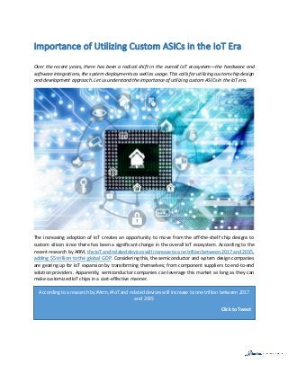
- 1. Importance of Utilizing Custom ASICs in the IoT Era Over the recent years, there has been a radical shift in the overall IoT ecosystem—the hardware and software integrations, the system deployments as well as usage. This calls for utilizing custom chip design and development approach. Let us understand the importance of utilizing custom ASICs in the IoT era. The increasing adoption of IoT creates an opportunity to move from the off-the-shelf chip designs to custom silicon since there has been a significant change in the overall IoT ecosystem. According to the recent research by ARM, the IoT and related devices will increase to one trillion between 2017 and 2035, adding $5 trillion to the global GDP. Considering this, the semiconductor and system design companies are gearing up for IoT expansion by transforming themselves; from component suppliers to end-to-end solution providers. Apparently, semiconductor companies can leverage this market as long as they can make customized IoT chips in a cost-effective manner. According to a research by #Arm, #IoT and related devices will increase to one trillion between 2017 and 2035 Click to Tweet
- 2. Why Custom ASIC for IoT Edge Products Rather than depending on using stock components in developing IoT edge products, ASIC design companies by utilizing custom silicon design in the targeted devices on the edge of IoT network can substantially enhance the functionality and offer greater design flexibility. Companies are now deploying custom ASIC platforms in IoT devices and are becoming fabless system companies. Moreover, using a custom ASIC business model approach, IoT edge products can be delivered as low cost, mid or highly integrated solutions. This is why, ASIC designers across vertical markets like medical devices, industrial and smart utilities, utilize custom ASIC designs to differentiate the IoT products and make them future proof as much as possible. How Custom ASIC Platforms Enhance IoT Products In IoT, connected devices face challenges of lower geometry design, form factor, sensor performance, testing and ensuring faster time-to-market with low cost. In order to overcome these challenges, ASIC designers utilize custom ASIC platforms with several mature technologies and techniques to ensure and maintain the performance of the IoT products. Here are the key ways custom ASIC platforms enhance the performance of IoT products: 1. Ultra-low Power Design: In order to maintain and reduce dynamic power consumption with different foundries, ASIC engineers follow power saving techniques which are applicable to lower geometry designs (180nm to 7nm / 5nm) a. Better Dynamic Power i. Clock gating and clock tree synthesis ii. Multibit register iii. Low power placement b. Power Leakage Savings i. Biasing ii. MCMM iii. Multi-Vt libraries c. Multi-Voltage i. Lower VDD operation ii. MV power domain iii. DVFS / AVS BONUS CONTENT Challenges and Opportunities for the Semiconductor Industry in the IoT WATCH THE VIDEO Role of Semiconductors in the IoT Era of Networking Industry
- 3. 2. Form Factor and Sensors: IoT products or space-constrained designs are following multiple component standards, where single small die size chip embed the micro-controllers, primary and rechargeable battery management system, sensors, wireless communication, secure copy protection in the smallest possible form factor. Here’s how ASIC engineers implement small form factor and sensors in developing IoT products: a. Low power and small form factor batteries: ASIC engineers choose a safe battery design which ensures durability, quality, and safety. Battery designs are available as thin as 0.37nm which continuously operate over a wide temperature range. For example, medical experts use new tech tools like injectable drugs which perform in effective time duration through safe and small powered patch. b. Sensors: ARM defined IoT as a sensor-enabled object that relates to the real world, where wireless analog functionalities are added to IoT products like wearables, mobiles, home and building automation application. For reliable integration and high-performance sensor solutions, ASIC engineers utilize the smart sensor interface (MEMS sensor element) to add to the ASIC design platform. 3. Turnkey Execution: In the era of miniaturization, ASIC turnkey execution delivers effective results for sports, mobility, healthcare, multi-market wireless, and multi-media solutions. One of the main objectives of turnkey services in IoT edge products is to improve quality, lifecycle, risk management process. Silicon Turkey ownership involves covering RTL to GDSII models and deploy the product when it is ready for operation. 4. Faster TTM at Low Cost: Due to the highly competitive situations in IoT market, ASIC companies have to launch their products on time to capture customer base, revenue, and market penetration. Fabless companies have evolved with faster methodologies to roll out custom ASIC in lesser time. This enables quick deployment of IoT products, resulting in successful IoT product launches. RELATED INFOGRAPHIC Bringing Internet of Things to Life with ARM Architecture DOWNLOAD CASE STUDY RTL to GDSII Turnkey ASIC for MEMS Applications
- 4. eInfochips has over two decades of experience in providing product engineering and ASIC design services on different technology nodes. It has enabled multiple Fortune 500 companies to deliver high-quality products on time. To know more, get in touch with us. About the Author: Komal Chauhan works in the marketing department at eInfochips, where she supports digital and content marketing activities for semiconductor and IoT applications.