SlideShare a Scribd company logo
1 of 41
Download to read offline
TheAllegroACS37800 power monitoring IC greatly simplifies
the addition of power monitoring to manyAC or DC powered
systems. The sensor may be powered from the same supply as
the system’s MCU, eliminating the need for multiple power
supplies. The device’s construction includes a copper conduction
path that generates a magnetic field proportional to applied
current. The magnetic field is sensed differentially to reject
errors introduced by common mode fields.
Allegro’s Hall-effect-based, galvanically isolated current sensing
technology achieves reinforced isolation ratings (4800 VRMS)
in a small PCB footprint. These features enable isolated current
sensing without expensive Rogowski coils, oversized current
transformers, isolated operational amplifiers, or the power
loss of shunt resistors.
The ACS37800 power monitoring IC offers key power
measurement parameters that can easily be accessed through its
SPI or I2C digital protocol interfaces. Dedicated and configurable
I/O pins for voltage/current zero crossing, undervoltage and
overvoltage reporting, and fast overcurrent fault detection are
available in I2C mode. User configuration of the IC is available
through on-chip EEPROM.
The ACS37800 is provided in a small low-profile surface
mount SOIC16 wide-body package, is lead (Pb) free, and is fully
calibrated prior to shipment from theAllegro factory. Customer
calibration can further increase accuracy in application.
ACS37800-DS, Rev. 3
MCO-0001004
• Accurate power monitoring for AC and DC applications
• UL 60950-1 (ed. 2) and UL 62368-1 (ed. 1) certified for
reinforced isolation up to 517 VRMS in a single package
• Accurate measurements of active, reactive, and apparent
power, as well as power factor
• Separate RMS and instantaneous measurements for both
voltage and current channels
• Two programmable averaging blocks
• 0.85 mΩ primary conductor resistance for low power loss
and high inrush current withstand capability
• Compatible with floating and non-floating GND
• Dedicated voltage or current zero crossing pin
• Fast, user-programmable overcurrent fault pin (5 µs typ.)
• User-programmable undervoltage and overvoltage RMS
thresholds
• 1 kHz bandwidth
• Current sensing range up to 90 A
• Options for I2C or SPI digital interface protocols
Isolated, Digital Output, Power Monitoring IC
with Zero-Crossing Detection, Overcurrent and Overvoltage Flagging
PACKAGE
Figure 1: Typical Application
FEATURES AND BENEFITS DESCRIPTION
Not to scale
ACS37800
IP
IP+
IP+
IP+
IP+
VINP
VINN
IP-
IP-
IP-
IP-
VCC
GND
1
2
3
4
5
6
7
8
16
15
14
13
12
11
10
9
L (N) N (L)
1 MΩ 1 MΩ
1 MΩ 1 MΩ
RSENSE
MCU
VCC
GND
To User
(
REINFORCED
ISOLATION
Linear
Regulator
ACS37800
SDA / MISO
SCL / SCLK
DIO_0 / MOSI
DIO_1 / CS
Isolated Power
Single Output
Supply
, etc.)
Flyback
RPULLUP
RPULLUP
I2
C
Only
16-pin SOICW (suffix MA)
March 17, 2022
CB Certificate Number:
US-32210-M1-UL
US-36315-UL
Isolated, Digital Output, Power Monitoring IC
with Zero-Crossing Detection, Overcurrent and Overvoltage Flagging
ACS37800
2
Allegro MicroSystems
955 Perimeter Road
Manchester, NH 03103-3353 U.S.A.
www.allegromicro.com
SELECTION GUIDE
Part Number VCC(typ) (V) IPR (A)
Communication
Protocol
TA (°C) Packing [1]
ACS37800KMACTR-015B5-SPI 5 ±15
SPI
–40 to 125
Tape and reel,
1000 pieces per reel,
3000 pieces per box
ACS37800KMACTR-030B3-SPI 3.3 ±30
ACS37800KMACTR-030B3-I2C 3.3 ±30
I2C
ACS37800KMACTR-090B3-I2C 3.3 ±90
[1] Contact Allegro for additional packing options.
ACS 37800 K MAC - 015 B 5
Supply Voltage:
5 – VCC = 5 V
3 – VCC = 3.3 V
Output Directionality:
B – Bidirectional
Current Sensing Range (A)
Package Designator
Operating Temperature Range
5 Digit Part Number
Allegro Current Sensor
TR
Packing Designator
Communication Protocol
- SPI
Isolated, Digital Output, Power Monitoring IC
with Zero-Crossing Detection, Overcurrent and Overvoltage Flagging
ACS37800
3
Allegro MicroSystems
955 Perimeter Road
Manchester, NH 03103-3353 U.S.A.
www.allegromicro.com
ISOLATION CHARACTERISTICS
Characteristic Symbol Notes Rating Unit
Dielectric Strength Test Voltage VISO
Agency type-tested for 60 seconds per UL 60950-1
(edition 2) and UL 62368-1 (edition 1); Production tested
at 3000 VRMS for 1 second, in accordance with UL 60950-1
(edition 2) and UL 62368-1 (edition 1)
4800 VRMS
Working Voltage for Basic Isolation VWVBI
Maximum approved working voltage for basic (single) isolation
according to UL 60950-1 (edition 2) and UL 62368-1 (edition 1)
1480 VPK or VDC
1047 VRMS
Working Voltage for Reinforced Isolation VWVRI
Maximum approved working voltage for reinforced isolation
according to UL 60950-1 (edition 2) and UL 62368-1 (edition 1)
730 VPK or VDC
517 VRMS
Clearance Dcl Minimum distance through air from IP leads to signal leads 7.5 mm
Creepage Dcr
Minimum distance along package body from IP leads to signal
leads
7.9 mm
Distance Through Insulation DTI Minimum internal distance through insulation 90 μm
Comparative Tracking Index CTI Material Group II 400 to 599 V
ABSOLUTE MAXIMUM RATINGS
Characteristic Symbol Notes Rating Units
Supply Voltage VCC 6.5 V
Reverse Supply Voltage VRCC –0.5 V
Input Voltage VINP, VINN VCC + 0.5 V
Reverse Input Voltage VRNP, VRNN –0.5 V
Digital I/O Voltage VDIO
SPI, I2C, and general purpose I/O
6 V
Reverse Digital I/O Voltage VRDIO –0.5 V
Maximum Continuous Current ICMAX TA = 25°C 60 A
Operating Ambient Temperature TA Range K –40 to 125 °C
Junction Temperature TJ(max) 165 °C
Storage Temperature Tstg –65 to 170 °C
THERMAL CHARACTERISTICS
Characteristic Symbol Test Conditions [1] Value Units
Package Thermal Resistance
(Junction to Ambient)
RθJA
Mounted on the Allegro ASEK37800 evaluation board with 750 mm2 of 4
oz. copper on each side, connected to pins 1 and 2, and to pins 3 and 4,
with thermal vias connecting the layers. Performance values include the
power consumed by the PCB.
23 °C/W
Package Thermal Resistance
(Junction to Lead)
RθJL Mounted on the Allegro ACS37800 evaluation board. 5 °C/W
[1] Refer to the Thermal Performance section below.
ESD RATINGS
Characteristic Symbol Notes Value Unit
Human Body Model VHBM Per JEDEC JS-001 ±5 kV
Charged Device Model VCDM Per JEDEC JS-002 ±1 kV
Isolated, Digital Output, Power Monitoring IC
with Zero-Crossing Detection, Overcurrent and Overvoltage Flagging
ACS37800
4
Allegro MicroSystems
955 Perimeter Road
Manchester, NH 03103-3353 U.S.A.
www.allegromicro.com
FUNCTIONAL BLOCK DIAGRAM
Bandgap
Reference
Fault Logic
Temperature
Sensor
IP+
IP–
VCC
GND
To All
Subcircuits
Hall Sensor Array
Metrology
Engine
I2C/SPI
Communication
EEPROM +
Charge Pump
Temperature
Compensation
Logic
DIGITAL SYSTEM
VINN
VINP
ADC
ADC
SDA / MISO
SCL / SCLK
DIO_0 / MOSI
DIO_1 / CS
V
I
Terminal List Table
Number Name
Description
I2C SPI
1, 2, 3, 4 IP+ Terminals for current being sensed; fused internally
5, 6, 7, 8 IP- Terminals for current being sensed; fused internally
9 DIO_1/CS Digital I/O 1 Chip Select (CS)
10 DIO_0/MOSI Digital I/O 0 MOSI
11 SCL  /SCLK SCL SCLK
12 SDA   /MISO SDA MISO
13 VCC Device power supply terminal
14 GND Device ground terminal
15 VINN Negative input voltage (always connect to GND)
16 VINP Positive input voltage
Pinout Diagram
1
IP+
2
IP+
3
IP+
4
IP+
5
IP-
6
IP-
7
IP-
8
IP- 9
10 DIO_0 / MOSI
11 SCL / SCLK
12 SDA / MISO
13 VCC
14 GND
15 VINN
16 VINP
DIO_1 / CS
PINOUT DIAGRAM AND TERMINAL LIST
Figure 2: Functional Block Diagram
Isolated, Digital Output, Power Monitoring IC
with Zero-Crossing Detection, Overcurrent and Overvoltage Flagging
ACS37800
5
Allegro MicroSystems
955 Perimeter Road
Manchester, NH 03103-3353 U.S.A.
www.allegromicro.com
Table of Contents
Features and Benefits............................................................ 1
Description........................................................................... 1
Package.............................................................................. 1
Typical Application................................................................. 1
Selection Guide.................................................................... 2
Absolute Maximum Ratings.................................................... 3
Isolation Characteristics......................................................... 3
ESD Ratings......................................................................... 3
Thermal Characteristics......................................................... 3
Functional Block Diagram...................................................... 4
Pinout Diagram and Terminal List............................................ 4
Electrical Characteristics........................................................ 6
15B5 Performance Characteristics.......................................... 8
30B3 Performance Characteristics.......................................... 9
90B3 Performance Characteristics........................................ 10
I2C Operating Characteristics................................................11
SPI Operating Characteristics............................................... 12
Theory of Operation............................................................ 13
Introduction..................................................................... 13
Voltage and Current Measurements................................... 13
Overcurrent Measurement Path......................................... 13
Trim Methods.................................................................. 13
Power Calculations.......................................................... 14
Operational Block Diagram................................................... 15
Configurable Settings....................................................... 16
Configuring the DIO Pins (I2C Devices) ............................. 16
Configuring the Device for AC Applications............................. 19
Device EEPROM Settings................................................. 19
Voltage Measurement....................................................... 19
Current Measurement....................................................... 20
Configuring the Device for DC Applications............................ 21
Device EEPROM Settings................................................. 21
Voltage Measurement....................................................... 21
Current Measurement....................................................... 21
RMS and Power Accuracy vs. Operation Point........................ 21
RMS and Power Output Error vs. Applied Input.................... 21
15B5 IRMS and Power Error ............................................ 22
30B3 IRMS and Power Error ............................................ 22
90B3 IRMS and Power Error ............................................ 22
Digital Communication......................................................... 23
Communication Interfaces................................................. 23
SPI................................................................................. 23
Registers and EEPROM................................................... 23
EEPROM Error Checking and Correction (ECC).................. 25
I2C Slave Addressing........................................................ 25
EEPROM/Shadow Memory Map........................................... 26
Register Details – EEPROM.............................................. 27
Volatile Memory Map........................................................ 32
Register Details – Volatile................................................. 33
Application Information........................................................ 38
Thermal Rise vs. Primary Current...................................... 38
ASEK37800 Evaluation Board Layout................................. 38
Recommended PCB Layout................................................. 39
Package Outline Drawing..................................................... 40
Isolated, Digital Output, Power Monitoring IC
with Zero-Crossing Detection, Overcurrent and Overvoltage Flagging
ACS37800
6
Allegro MicroSystems
955 Perimeter Road
Manchester, NH 03103-3353 U.S.A.
www.allegromicro.com
Characteristic Symbol Test Conditions Min. Typ. Max. Unit
ELECTRICAL CHARACTERISTICS
Supply Voltage VCC
5 V variant 4.5 5 5.5 V
3.3 V variant 2.97 3.3 3.63 V
Supply Current ICC
VCC(min) ≤ VCC ≤ VCC(max), no load on
output pins
– 12 15 mA
Supply Bypass Capacitor CBYPASS VCC to GND recommended 0.1 – – µF
Power-On Time tPO – 90 – µs
VOLTAGE INPUT BUFFER
Differential Input Range ΔVINR ΔVIN = VINP – VINN(GND) –250 – 250 mV
Dynamic Input Frequency fdyn_in bypass_n_en = 0 35 – 300 Hz
VOLTAGE CHANNEL ADC
Sample Frequency fS_V – 32 – kHz
Number of Bits ADCV_B – 16 – bits
ADC Fullscale ADCV_FS ΔVIN = ±250 mV, VINN= GND –27500 – 27500 codes
Sensitivity Sens(V) ΔVINR(min) < ΔVIN < ΔVINR(max) – 110 – LSB / mV
Voltage Channel Power Supply Error
PSEV_O
Ratio of change on VCC to change in
offset at DC, 100% ±10% VCC(typ)
–7 – 7
codes /
%VCC
PSEV_S
Ratio of change on VCC to change in
sensitivity at DC, 100% ±10% VCC(typ)
–0.1 – 0.1 % / %VCC
Voltage Channel Power Supply Rejection
Ratio
PSRRV_O
Ratio of change on VCC to change in
offset, 10 Hz to 10 kHz, 10% VCC(pk-pk)
60 70 – dB
PSRRV_S
Ratio of change on VCC to change in
sensitivity, 10 Hz to 10 kHz, 10% VCC(pk-pk)
60 75 – dB
VOLTAGE CHANNEL
Internal Bandwidth BW – 1 – kHz
RMS Noise NV Input referred – ±0.3 – mV
Linearity Error ELIN_V – ±0.2 – %
CURRENT CHANNEL
Sample Frequency fS_C – 32 – kHz
Number of Bits ADCI_B – 16 – bits
ADC Fullscale ADCI_FS IP = IPR(min) or IPR(max) –27500 – 27500 codes
Current Channel Power Supply Error
PSEI_O
Ratio of change on VCC to change in
offset at DC, 100% ±10% VCC(typ)
–60 – 60
codes /
%VCC
PSEI_S
Ratio of change on VCC to change in
sensitivity at DC, 100% ±10% VCC(typ)
–0.3 – 0.3 % / %VCC
Current Channel Power Supply Rejection
Ratio
PSRRI_O
Ratio of change on VCC to change in
offset, 10 Hz to 10 kHz, 10% VCC(pk-pk)
60 65 – dB
PSRRI_S
Ratio of change on VCC to change in
sensitivity, 10 Hz to 10 kHz, 10% VCC(pk-pk)
20 40 – dB
Internal Bandwidth BW – 1 – kHz
Primary Conductor Resistance RIP TA = 25°C – 0.85 – mΩ
Continued on next page...
COMMON ELECTRICAL CHARACTERISTICS [1]: Valid through the full range of TA and VCC = VCC(typ), unless otherwise specified
Isolated, Digital Output, Power Monitoring IC
with Zero-Crossing Detection, Overcurrent and Overvoltage Flagging
ACS37800
7
Allegro MicroSystems
955 Perimeter Road
Manchester, NH 03103-3353 U.S.A.
www.allegromicro.com
Characteristic Symbol Test Conditions Min. Typ. Max. Unit
CURRENT CHANNEL (continued)
RMS Noise NI Input referred – ±0.1 – A
Linearity Error ELIN_I – ±1.5 – %
OVERCURRENT FAULT CHARACTERISTICS
Fault Response Time tRF
Time from IP rising above IFAULT until
VFAULT < VFAULT(max) for a current
step from 0 to 1.2 × IFAULT; 10 kΩ and
100 pF from DIO_1 to ground;
fltdly = 0
– 5 – μs
Internal Bandwidth BW – 200 – kHz
Fault Hysteresis [2] IHYST – 0.06 × FS – A
Fault Range IFAULT Set using fault field in EEPROM 0.65 × FS – 2.00 × FS A
VOLTAGE ZERO CROSSING
Voltage Zero-Crossing Delay td – 250 – µs
DIO PINS
DIO Output High Level VOH(DIO) VCC = 3.3 V 3 – – V
DIO Output Low Level VOL(DIO) VCC = 3.3 V – – 0.3 V
DIO Input Voltage for Address Selection 0 VADD0 VCC = 3.3 V – 0 – V
DIO Input Voltage for Address Selection 1 VADD1 VCC = 3.3 V – 1.1 – V
DIO Input Voltage for Address Selection 2 VADD2 VCC = 3.3 V – 2.2 – V
DIO Input Voltage for Address Selection 3 VADD3 VCC = 3.3 V – 3.3 – V
[1] Device may be operated at higher primary current levels (IP), ambient temperatures (TA), and internal leadframe temperatures, provided that the maximum junction
temperature (TJ(max)) is not exceeded.
[2] After IP goes above IFAULT, tripping the internal fault comparator, IP must go below IFAULT – IHYST before the internal fault comparator will reset.
COMMON ELECTRICAL CHARACTERISTICS [1] (continued): Valid through the full range of TA and VCC = VCC(typ),
unless otherwise specified
Isolated, Digital Output, Power Monitoring IC
with Zero-Crossing Detection, Overcurrent and Overvoltage Flagging
ACS37800
8
Allegro MicroSystems
955 Perimeter Road
Manchester, NH 03103-3353 U.S.A.
www.allegromicro.com
Characteristic Symbol Test Conditions Min. Typ. [1] Max. Unit
GENERAL CHARACTERISTICS
Nominal Supply Voltage VCC(typ) – 5 – V
NOMINAL PERFORMANCE – FACTORY CURRENT CHANNEL
Current Sensing Range IPR –15 – 15 A
Sensitivity Sens(I) IPR(min) < IP < IPR(max) – 1833.3 – LSB/A
NOMINAL PERFORMANCE – INPUT REFERRED FACTORY POWER (POWER SEEN BY THE DEVICE) [2]
Active Power Sensitivity SensPd_act – 6.15 – LSB/mW
Imaginary Power Sensitivity SensPd_img – 12.31 – LSB/mVAR
Apparent Power Sensitivity SensPd_app – 12.31 – LSB/mVA
TOTAL OUTPUT ERROR COMPONENTS [3] – CURRENT CHANNEL
Sensitivity Error ESENS(I)
Measured at IP = IPR(max), TA = 25°C to 125°C – ±1.1 – %
Measured at IP = IPR(max), TA = –40°C to 25°C – ±1.5 – %
Offset Error EO(I)
IP = 0 A, TA = 25°C to 125°C – ±720 – LSB
IP = 0 A, TA = –40°C to 25°C – ±780 – LSB
Total Output Error ETOT(I)
Measured at IP = IPR(max), TA = 25°C to 125°C – ±2.1 – %
Measured at IP = IPR(max), TA = –40°C to 25°C – ±2.7 – %
TOTAL OUTPUT ERROR COMPONENTS [3] – VOLTAGE CHANNEL
Sensitivity Error ESENS(V)
Measured at ΔVIN = ΔVINR(max),
TA = 25°C to 125°C
– ±1.2 – %
Measured at ΔVIN = ΔVINR(max),
TA = –40°C to 25°C
– ±1.2 – %
Offset Error EO(V)
ΔVIN = 0 mV, TA = 25°C to 125°C – ±55 – LSB
ΔVIN = 0 mV, TA = –40°C to 25°C – ±55 – LSB
Total Output Error ETOT(V)
Measured at ΔVIN = ΔVINR(max),
TA = 25°C to 125°C
– ±1.4 – %
Measured at ΔVIN = ΔVINR(max),
TA = –40°C to 25°C
– ±1.4 – %
ACCURACY PERFORMANCE – ACTIVE POWER
Total Output Error ETOT(P)
IP = IPR(max), measured at ΔVIN = ΔVINR(max),
TA = 25°C to 125°C
– ±2.1 – %
IP = IPR(max), measured at ΔVIN = ΔVINR(max),
TA = –40°C to 25°C
– ±3 – %
[1] Typical values are mean ±3 sigma.
[2] These sensitivity characteristics are referred to the inputs seen by the device, i.e. the voltage channel resistor divider must be accounted to determine the system sensi-
tivies.
[3] ETOT = ESENS + 100 x VOE/(Sens x IP)
ACS37800KMAC-015B5 PERFORMANCE CHARACTERISTICS: Valid through the full operating temperature range,
TA = –40°C to 125°C, CBYPASS = 0.1 µF, and VCC = 5 V, unless otherwise specified
Isolated, Digital Output, Power Monitoring IC
with Zero-Crossing Detection, Overcurrent and Overvoltage Flagging
ACS37800
9
Allegro MicroSystems
955 Perimeter Road
Manchester, NH 03103-3353 U.S.A.
www.allegromicro.com
Characteristic Symbol Test Conditions Min. Typ. [1] Max. Unit
GENERAL CHARACTERISTICS
Nominal Supply Voltage VCC(typ) – 3.3 – V
NOMINAL PERFORMANCE – CURRENT CHANNEL
Current Sensing Range IPR –30 – 30 A
Sensitivity Sens(I) IPR(min) < IP < IPR(max) – 916.7 – LSB/A
NOMINAL PERFORMANCE – INPUT REFERRED FACTORY POWER (POWER SEEN BY THE DEVICE) [2]
Active Power Sensitivity SensPd_act – 3.08 – LSB/mW
Imaginary Power Sensitivity SensPd_img – 6.15 – LSB/mVAR
Apparent Power Sensitivity SensPd_app – 6.15 – LSB/mVA
TOTAL OUTPUT ERROR COMPONENTS [3] – CURRENT CHANNEL
Sensitivity Error ESENS(I)
Measured at IP = IPR(max), TA = 25°C to 125°C – ±1 – %
Measured at IP = IPR(max), TA = –40°C to 25°C – ±1.5 – %
Offset Error EO(I)
IP = 0 A, TA = 25°C to 125°C – ±510 – LSB
IP = 0 A, TA = –40°C to 25°C – ±570 – LSB
Total Output Error ETOT(I)
Measured at IP = IPR(max), TA = 25°C to 125°C – ±2 – %
Measured at IP = IPR(max), TA = –40°C to 25°C – ±2.7 – %
TOTAL OUTPUT ERROR COMPONENTS [3] – VOLTAGE CHANNEL
Sensitivity Error ESENS(V)
Measured at ΔVIN = ΔVINR(max),
TA = 25°C to 125°C
– ±0.75 – %
Measured at ΔVIN = ΔVINR(max),
TA = –40°C to 25°C
– ±0.75 – %
Offset Error EO(V)
ΔVIN = 0 mV, TA = 25°C to 125°C – ±55 – LSB
ΔVIN = 0 mV, TA = –40°C to 25°C – ±55 – LSB
Total Output Error ETOT(V)
Measured at ΔVIN = ΔVINR(max),
TA = 25°C to 125°C
– ±1 – %
Measured at ΔVIN = ΔVINR(max),
TA = –40°C to 25°C
– ±1 – %
ACCURACY PERFORMANCE – ACTIVE POWER
Total Output Error ETOT(P)
IP = IPR(max), measured at ΔVIN = ΔVINR(max),
TA = 25°C to 125°C
– ±2.1 – %
IP = IPR(max), measured at ΔVIN = ΔVINR(max),
TA = –40°C to 25°C
– ±3 – %
[1] Typical values are mean ±3 sigma.
[2] These sensitivity characteristics are referred to the inputs seen by the device, i.e. the voltage channel resistor divider must be accounted to determine the system sensi-
tivies.
[3] ETOT = ESENS + 100 x VOE/(Sens x IP)
ACS37800KMAC-030B3 PERFORMANCE CHARACTERISTICS: Valid through the full operating temperature range,
TA = –40°C to 125°C, CBYPASS = 0.1 µF, and VCC = 3.3 V, unless otherwise specified
Isolated, Digital Output, Power Monitoring IC
with Zero-Crossing Detection, Overcurrent and Overvoltage Flagging
ACS37800
10
Allegro MicroSystems
955 Perimeter Road
Manchester, NH 03103-3353 U.S.A.
www.allegromicro.com
Characteristic Symbol Test Conditions Min. Typ. [1] Max. Unit
GENERAL CHARACTERISTICS
Nominal Supply Voltage VCC(typ) – 3.3 – V
NOMINAL PERFORMANCE – CURRENT CHANNEL
Current Sensing Range IPR –90 – 90 A
Sensitivity Sens(I) IPR(min) < IP < IPR(max) – 305.6 – LSB/A
NOMINAL PERFORMANCE – INPUT REFERRED FACTORY POWER (POWER SEEN BY THE DEVICE) [2]
Active Power Sensitivity SensPd_act – 1.03 – LSB/mW
Imaginary Power Sensitivity SensPd_img – 2.05 – LSB/mVAR
Apparent Power Sensitivity SensPd_app – 2.05 – LSB/mVA
TOTAL OUTPUT ERROR COMPONENTS [3] – CURRENT CHANNEL
Sensitivity Error ESENS(I)
Measured at IP = IPR(max), TA = 25°C to 125°C – ±1 – %
Measured at IP = IPR(max), TA = –40°C to 25°C – ±1.5 – %
Offset Error EO(I)
IP = 0 A, TA = 25°C to 125°C – ±180 – LSB
IP = 0 A, TA = –40°C to 25°C – ±210 – LSB
Total Output Error ETOT(I)
Measured at IP = 45 A, TA = 25°C to 125°C – ±2 – %
Measured at IP = 45 A, TA = –40°C to 25°C – ±2.6 – %
TOTAL OUTPUT ERROR COMPONENTS [3] – VOLTAGE CHANNEL
Sensitivity Error ESENS(V)
Measured at ΔVIN = ΔVINR(max),
TA = 25°C to 125°C
– ±0.75 – %
Measured at ΔVIN = ΔVINR(max),
TA = –40°C to 25°C
– ±0.75 – %
Offset Error EO(V)
ΔVIN = 0 mV, TA = 25°C to 125°C – ±55 – LSB
ΔVIN = 0 mV, TA = –40°C to 25°C – ±55 – LSB
Total Output Error ETOT(V)
Measured at ΔVIN = ΔVINR(max),
TA = 25°C to 125°C
– ±1 – %
Measured at ΔVIN = ΔVINR(max),
TA = –40°C to 25°C
– ±1 – %
ACCURACY PERFORMANCE – ACTIVE POWER
Total Output Error ETOT(P)
IP = 45 A, measured at ΔVIN = ΔVINR(max),
TA = 25°C to 125°C
– ±1.3 – %
IP = 45 A, measured at ΔVIN = ΔVINR(max),
TA = –40°C to 25°C
– ±2.1 – %
[1] Typical values are mean ±3 sigma.
[2] These sensitivity characteristics are referred to the inputs seen by the device, i.e. the voltage channel resistor divider must be accounted to determine the system sensi-
tivies.
[3] ETOT = ESENS + 100 x VOE/(Sens x IP)
ACS37800KMAC-090B3 PERFORMANCE CHARACTERISTICS: Valid through the full operating temperature range,
TA = –40°C to 125°C, CBYPASS = 0.1 µF, and VCC = 3.3 V, unless otherwise specified
Isolated, Digital Output, Power Monitoring IC
with Zero-Crossing Detection, Overcurrent and Overvoltage Flagging
ACS37800
11
Allegro MicroSystems
955 Perimeter Road
Manchester, NH 03103-3353 U.S.A.
www.allegromicro.com
Characteristic Symbol Test Conditions Min. Typ. Max. Unit
I2C INTERFACE CHARACTERISTICS [2]
Bus Free Time Between Stop and Start tBUF 1.3 – – µs
Hold Time Start Condition thdSTA 0.6 – – µs
Setup Time for Repeated Start Condition tsuSTA 0.6 – – µs
SCL Low Time tLOW 1.3 – – µs
SCL High Time tHIGH 0.6 – – µs
Data Setup Time tsuDAT 100 – – µs
Data Hold Time thdDAT 0 – 900 µs
Setup Time for Stop Condition tsuSTO 0.6 – – µs
Logic Input Low Level (SDA, SCL pins) VIL – – 30 %VCC
Logic Input High Level (SDA, SCL pins) VIH 70 – – %VCC
Logic Input Current IIN Input voltage on SDA or SCL = 0 V to VCC –1 – 1 µA
Output Low Voltage (SDA) VOL SDA sinking = 1.5 mA – – 0.36 V
Clock Frequency (SCL pin) fCLK – – 400 kHz
Output Fall Time (SDA pin) tf REXT = 2.4 kΩ, CB = 100 pF – – 250 ns
I2C Pull-Up Resistance REXT 2.4 10 – kΩ
Total Capacitive Load for Each of SDA and
SCL Buses
CB – – 20 pF
[1] Validated by characterization and design.
[2] These values are ratiometric to the supply voltage. I2C Interface Characteristics are ensured by design and not factory tested.
xKMACTR-I2C OPERATING CHARACTERISTICS [1]: Valid through the full range of TA, VCC = VCC(typ), REXT = 10 kΩ,
unless otherwise specified
tsuSTA
tsuDAT
tLOW
tsuSTO
thdSTA thdDAT
tHIGH
tBUF
SDA
SCL
Figure 3: I2C Interface Timing
Isolated, Digital Output, Power Monitoring IC
with Zero-Crossing Detection, Overcurrent and Overvoltage Flagging
ACS37800
12
Allegro MicroSystems
955 Perimeter Road
Manchester, NH 03103-3353 U.S.A.
www.allegromicro.com
Characteristic Symbol Test Conditions Min. Typ. Max. Unit
SPI INTERFACE CHARACTERISTICS
Digital Input High Voltage VIH
MOSI, SCLK, CS pins, VCC = 3.3 V 2.8 – 3.63 V
MOSI, SCLK, CS pins, VCC = 5 V 4 – 5.5 V
Digital Input Low Voltage VIL MOSI, SCLK, CS pins – – 0.5 V
SPI Output High Voltage VOH
MISO pin, CL = 20 pF, TA = 25°C,
VCC(typ) = 3.3 V
2.8 3.3 3.8 V
MISO pin, CL = 20 pF, TA = 25°C,
VCC(typ) = 5 V
4 5 5.5 V
SPI Output Low Voltage VOL MISO pin, CL = 20 pF, TA = 25°C – 0.3 0.5 V
SPI Clock Frequency fSCLK MISO pin, CL = 20 pF 0.1 – 10 MHz
SPI Frame Rate tSPI 5.8 – 588 kHz
Chip Select to First SCLK Edge tCS
Time from CS going low to SCLK falling
edge
50 – – ns
Data Output Valid Time tDAV Data output valid after SCLK falling edge – 40 – ns
MOSI Setup Time tSU Input setup time before SCLK rising edge 25 – – ns
MOSI Hold Time tHD Input hold time after SCLK rising edge 50 – – ns
SCLK to CS Hold Time tCHD
Hold SCLK high time before CS rising
edge
5 – – ns
Load Capacitance CL Loading on digital output (MISO) pin – – 20 pF
[1] Validated by characterization and design.
xKMATR-SPI OPERATING CHARACTERISTICS [1]: Valid through the full range of TA, VCC = VCC(typ), unless otherwise specified
CSN
SCLK
MOSI
MISO
tCS
tSU tHD
tDAV
tCHD >tCS
Figure 4: SPI Timing
Isolated, Digital Output, Power Monitoring IC
with Zero-Crossing Detection, Overcurrent and Overvoltage Flagging
ACS37800
13
Allegro MicroSystems
955 Perimeter Road
Manchester, NH 03103-3353 U.S.A.
www.allegromicro.com
THEORY OF OPERATION
Introduction
The ACS37800 provides a simple solution for voltage, current,
and power monitoring in 60 Hz AC and DC applications and is
particularly well suited for high isolation. The voltage is mea-
sured by resistor dividing it down to fit the input range of the
on-board voltage sense amplifier, as well as to add isolation.
The current is measured using the integrated current loop and
galvanically isolated Hall sensor. Both analog signals are then
sampled using high accuracy ADCs before entering the digital
system. Here, the metrology engine is used to determine fre-
quency, calculate RMS values of current, voltage, and power, as
well as provide a range of averaging and configuration options.
One can choose to read out all the different information provided
using SPI or I2C. When using I2C, there are also options for
using some of the digital I/O pins for overcurrent or zero cross-
ing detection. Overall, with a high degree of configurability and
integrated features, the ACS37800 can fit most power monitoring
applications. The following sections will help explain in more
detail these features and configuration options, as well as how to
best use the ACS37800 for particular applications.
Voltage and Current Measurements
The main signal paths for the current and voltage measurement,
through the ADCs and internal filtering, have a bandwidth of
1 kHz and an update rate of 32 kHz. These “instantaneous”
current and voltage measurements are stored in the icodes and
vcodes fields. The instantaneous apparent power, which is the
product of icodes and vcodes, is stored in the field pinstant.
Overcurrent Measurement Path
A separate filter on the current ADC is used to create a lower
resolution but higher bandwidth sample rate measurement of the
current to be used for overcurrent detection. This filter outputs a
12-bit word at a 1 MHz update rate and 200 kHz bandwidth. The
overcurrent fault logic compares this auxiliary current value to the
user-defined overcurrent fault threshold, defined by the field fault.
It is important to note that the trim for the main 16-bit current path
is also applied to the overcurrent path, such that the overcurrent
fault has the same level of accuracy as the main signal path.
Trim Methods
The trim logic for the voltage and current channels is depicted in
Figure 5 and Figure 6. Refer to the Register Details section for
more information regarding trim fields. In general, each chan-
nel, voltage and current, is trimmed for gain and offset both at
room and over temperature. This trim is done before the icodes
and vcodes registers. The user has the ability to trim the nominal
room temperature value.
Figure 5: Voltage Channel Trim Flow
Figure 6: Current Channel Trim Flow
Delay
Z-x
chan_del_sel
ichan_del_en
Satura�on
Gain Trim
VchanGainSel
Offset Trim
+
+
+
+
vchan_offset_code
vqvo_tc
vcodes
adc_out_v
Factory
Trim
Satura�on
Gain Trim
sns_fine
sns_tc
Offset Trim
+
+
+
+
qvo_fine
qvo_tc
Delay
Z-x
chan_del_sel
ichan_del_en
icodes
adc_out_i
Factory
Trim
Isolated, Digital Output, Power Monitoring IC
with Zero-Crossing Detection, Overcurrent and Overvoltage Flagging
ACS37800
14
Allegro MicroSystems
955 Perimeter Road
Manchester, NH 03103-3353 U.S.A.
www.allegromicro.com
Power Calculations
VOLTAGE ZERO CROSSING
The RMS and power calculations of the ACS37800 are calcu-
lated over a window of N samples. By default, this window is
calculated dynamically based on the zero crossings of the voltage
signal. A rising voltage zero crossing triggers the start of a new
window. N then increases with each 32 kHz sample until the next
rising voltage zero crossing, recording the current and voltage
readings at each sample. This ends the calculation window, and
all RMS and power calculations are performed on the saved data.
During this time, the next calculation window is started.
Voltage zero crossings are detected with time-based hysteresis
that removes the possibility of noise causing multiple zero cross-
ings to be reported at each true zero crossing.
IRMS AND VRMS
The cycle-by-cycle calculation of the root mean square of both
the current and voltage channels is:
IRMS =
∑
N
n = N – 1
n = 0 In
2
VRMS =
∑
N
n = N – 1
n = 0 Vn
2
where In (icodes) and Vn (vcodes) are the instantaneous measure-
ments of current and voltage, respectively.
APPARENT POWER
The magnitude of the complex power being measured; calculated
at the end of each cycle is:
|S| = IRMS × VRMS
ACTIVE POWER
The real component of power being measured, calculated cycle
by cycle is:
PACTIVE =
∑
N
n = N – 1
n = 0 Pn
Pn = In × Vn
REACTIVE POWER
The imaginary component of power being measured, calculated
at the end of each cycle is:
Q = S2
– PACTIVE
2
POWER FACTOR
The magnitude of the ratio of the real power to apparent power,
calculated at the end of each cycle is:
|PF| =
|S|
PACTIVE
LEADING OR LAGGING POWER FACTOR
The current leading or lagging the voltage is communicated as a
single bit, posangle. This bit represents the sign of the reactive
power. The sign of the reactive power is determined by compar-
ing the timing of the zero crossings of the current and voltage. As
such, it is only meaningful in the case of a linear load.
The sign of the reactive power, posangle, along with the sign of
the power factor, pospf, can be used to determine whether the
load is inductive or capacitive, as well as whether power is being
generated or consumed. This is shown in the four-quadrant figure
below (refer to Figure 7).
Imaginary
Real
POSPF = 1
POSANG = 1
POSPF = 0
POSANG = 0
POSPF = 0
POSANG = 1
POSPF = 1
POSANG = 0
Lagging
Leading
Capacitive and
Generating
Capacitive and
Consuming
Inductive and
Consuming
Inductive and
Generating
Figure 7: Four Quadrant, Power Factor
Figure 8: Power Triangle
Apparent Power, S = VI
Active Power, P = VI cosФ
Reactive
Power,
Q
=
VI
sinФ
Ф
S = P 2
+ Q 2
Isolated, Digital Output, Power Monitoring IC
with Zero-Crossing Detection, Overcurrent and Overvoltage Flagging
ACS37800
15
Allegro MicroSystems
955 Perimeter Road
Manchester, NH 03103-3353 U.S.A.
www.allegromicro.com
Factory Trimmed
Current
ADC
RSENSE
ΣRISO
+ RSENSE
VLINE
Voltage
ADC
Temperature
Compensation
Digital
Filter
Voltage Zero
Crossing
vrms
papparent
irms
ovrms
uvrms
pinstant
pactive
pimag
Averaging
vrmsavgonesec
vrmsavgonemin
irmsavgonemin
irmsavgonesec
pactiveavgonesec
pactiveavgonemin
0
1
0
1
iavgselen
pavgselen
RMS
and
Power
Calculations
O/UVRMS
Flag
Channel
Delay
Control icodes
vcodes
X
icodes
vcodes
Zero
Crossing
Flag
vrms
irms
pactive
Voltage and
Current
Measurement
RMS, and Power
Calculation
Averaging and
VRMS Flagging
IP+
IP–
Overcurrent
Fault
Comparator
fault
fault out
Register
Voltage data Current data Power data Control
Output Operation
FAULT data
pospf
posangle
OPERATIONAL BLOCK DIAGRAM
Figure 9: Operational Block Diagram
Isolated, Digital Output, Power Monitoring IC
with Zero-Crossing Detection, Overcurrent and Overvoltage Flagging
ACS37800
16
Allegro MicroSystems
955 Perimeter Road
Manchester, NH 03103-3353 U.S.A.
www.allegromicro.com
Configurable Settings
PHASE DELAY
Phase delay may be introduced on either the voltage or current
channel to account for known phase delay at other points in the
system using the ichan_del_en and chan_ del_sel fields. ichan_
del_en determines if the voltage channel or current channel will
be delayed. The chosen channel will be delayed by the configured
amount in chan_del_sel, up to 5° of delay.
AVERAGING CHANNEL
The ACS37800 contains two averaging paths. VRMS, IRMS, and
PACTIVE can be routed to these average blocks as shown in Figure 9
using iavgselen and pavgselen.
AVERAGING TIME
Each averaging path on the ACS37800 consists of two averag-
ing blocks that each allow for a configurable number of averages
based on the EEPROM fields rms_avg_1 and rms_avg_2.
The output of the first averaging block feeds into the input of the
second averaging block. The output of each block is accessible
for each channel.
OVERVOLTAGE AND UNDERVOLTAGE DETECTION
FOR VRMS
This device has programmable overvoltage and undervoltage
RMS flags that will signal when the vrms is above or below the
respective thresholds. The vrms is compared to the overvoltage
and undervoltage RMS thresholds set by the fields overvreg and
undervreg to determine a flag condition. The number of suc-
cessive sample sets required to trigger either the overvoltage or
undervoltage RMS flag can be set by the vevent_cycs field.
The ovrms and uvrms flags can be routed to the DIO pins when
the device is used in I2C mode. See Configuring the DIO Pins.
OVERCURRRENT DETECTION FOR INSTANTA-
NEOUS CURRENT
The overcurrent fault threshold may be set from 0.65 × IPR to
2.0 × IPR. The user sets the trip point with the field fault. The
user can add a digital delay to the overcurrent fault with the field
flt_dly. Up to 32 µs delay can be added to the overcurrent fault.
BYPASSING THE DYNAMIC FRAMING OF THE RMS
CALCULATION WINDOW
By default, the ACS37800 dynamically calculates the value of
N to be used in the RMS and power calculations based on the
zero crossings on the voltage channel. This functionality can be
disabled using the bypass_n_en field.
When bypass_n_en = 1, it is important to define the number of
samples used to calculate RMS. This can be done in the field
n. The field n is the number of 32 kHz samples that are used to
calculate the RMS. The minimum effective n that is used when
calculating RMS is 4. If a value of less than 4 is chosen for n,
then 4 is internally used. The first useable RMS calculation on
start up with bypass_n_en = 1 is after 2 × n samples.
Configuring the DIO Pins (I2C Devices)
FLAGS TO BE ROUTED TO THE DIO PINS
When the device is configured to be in I2C mode (comm_sel in
EEPROM = 1), pins 9 and 10 become digital I/O pins, DIO_1
and DIO_0, respectively. The digital I/O pins are low true, mean-
ing that a voltage below the DIO Output Low Level maximum
(VOL(DIO)max) is to be interpreted as logic 1 and a voltage above
DIO Output High Level minimum (VOH(DIO)min) is to be inter-
preted as a logic 0. The Digital I/O pins can be configured in
EEPROM to represent the following functions:
DIO_O
dio_0_sel value (EEPROM) Function
0 ZC: zero crossing
1 ovrms: the VRMS overvoltage flag
2 uvrms: The VRMS undervoltage flag
3
The OR of ovrms and uvrms (if either flag is
triggered, the DIO_0 pin will be asserted)
OVRMS
UVRMS
OVRMS
UVRMS
OCF_LAT
OCF
ZC
DIO_0
DIO_1
CS
MOSI
DIO_1 / CS
DIO_0 / MOSI
DIO_0_Sel[0..1] Comm_Sel
DIO_1_Sel[0..1] Comm_Sel
DIO_1
dio_1_sel value (EEPROM) Function
0 OCF: Overcurrent fault
1 uvrms: The VRMS undervoltage flag
2 ovrms: The VRMS overvoltage flag
3
The OR of ovrms and uvrms, and OCF_LAT [Latched
Overcurrent Fault] (if any of the three flags are
triggered, the DIO_1 pin will be asserted)
OVRMS
UVRMS
OVRMS
UVRMS
OCF_LAT
OCF
ZC
DIO_0
DIO_1
CS
MOSI
DIO_1 / CS
DIO_0 / MOSI
DIO_0_Sel[0..1] Comm_Sel
DIO_1_Sel[0..1] Comm_Sel
Isolated, Digital Output, Power Monitoring IC
with Zero-Crossing Detection, Overcurrent and Overvoltage Flagging
ACS37800
17
Allegro MicroSystems
955 Perimeter Road
Manchester, NH 03103-3353 U.S.A.
www.allegromicro.com
ZERO CROSSING OUTPUT CONFIGURATIONS
The dynamic calculation of N for the RMS and power calcula-
tions uses exclusively the voltage zero crossing, but both current
and voltage zero crossing can be flagged and reported on the DIO
pins.
Voltage Zero Crossing (VZC)
The voltage zero crossing has two basic modes of operation,
pulse mode and square wave mode.
Pulse Mode – VZC
In pulse mode, a voltage zero crossing is reported as a short
pulse. There are three available configurations to customize the
voltage zero crossing pulse mode operation: rising or falling edge
selection, every edge selection, and pulse width.
Rising Edge or Falling Edge Aligned Pulse
The EEPROM field zerocrossedgesel is used to select whether
the zero crossing output pulses are aligned to the rising zero
crossing of the voltage channel or the falling zero crossing of the
voltage channel.
Figure 10: zerocrossedgesel = 0, Falling Zero Crossing
Figure 11: zerocrossedgesel = 1, Rising Zero Crossing
Pulse Every Edge
The EEPROM field halfcycle_en is used to output a pulse at
every zero crossing.
Figure 12: halfcycle_en = 1, Both Rising and Falling
Zero Crossings Signaled
Pulse Width Selection
The EEPROM field delaycnt_sel is used to select the width of the
voltage zero crossing pulse.
Table 1: delaycnt_sel
Range Value Units
0 32 µs
1 256 µs
Isolated, Digital Output, Power Monitoring IC
with Zero-Crossing Detection, Overcurrent and Overvoltage Flagging
ACS37800
18
Allegro MicroSystems
955 Perimeter Road
Manchester, NH 03103-3353 U.S.A.
www.allegromicro.com
Square Wave Mode
Square wave mode can be configured using the EEPROM field
squarewave_en. In square wave mode, a voltage zero crossing
is reported as a square wave that changes state on each reported
zero crossing. The zerocrossedgesel EEPROM field can be used
to align the low to high transition of the flag with either the rising
voltage zero crossing or the falling voltage zero crossing.
Figure 13: zerocrossedgesel = 0, Square Wave Mode
Figure 14: zerocrossedgesel = 1, Square Wave Mode
Current Zero Crossing (CZC)
The current zero crossing function can be enabled using the
EEPROM field zerocrosschansel. When the zero crossing flag
is configured to flag zero crossings of the current path, this has
no effect on the RMS and power calculations; the voltage zero
crossing is still used for these calculations.
The current zero crossing has just one basic mode of operation:
pulse mode.
Pulse Mode – CZC
In pulse mode, a current zero crossing is reported as a short
pulse. There are three available configurations to customize the
current zero crossing pulse mode operation: rising or falling edge
selection, every edge selection, and pulse width.
Rising Edge or Falling Edge Aligned Pulse
The EEPROM field zerocrossedgesel is used to select whether
the zero crossing output pulses are aligned to the rising zero
crossing of the current channel or the falling zero crossing of the
current channel.
Figure 15: zerocrossedgesel = 0, Falling Zero Crossing
Figure 16: zerocrossedgesel = 1, Rising Zero crossing
Isolated, Digital Output, Power Monitoring IC
with Zero-Crossing Detection, Overcurrent and Overvoltage Flagging
ACS37800
19
Allegro MicroSystems
955 Perimeter Road
Manchester, NH 03103-3353 U.S.A.
www.allegromicro.com
Pulse Every Edge
The EEPROM field halfcycle_en is used to output a pulse at
every zero crossing.
Figure 17: halfcycle_en = 1, Both Rising and Falling
Zero Crossings Signaled
CONFIGURING THE DEVICE FOR AC APPLICATIONS
Device EEPROM Settings
For AC power monitoring applications using the ACS37800, the
following device settings are recommended:
DYNAMIC CALCULATION OF N
Set bypass_n_en = 0 (default). This setting enables the device to
dynamically calculate N based off the voltage zero crossings. See
the Register Details – EEPROM section for additional details.
Voltage Measurement
RECOMMENDED APPLICATION CIRCUITS
An important aspect to consider when designing in the
ACS37800 into AC applications is the design of the voltage mea-
surement path. Typically, a resistor divider network is employed
to provide both isolation and transform the high voltage signal
into the ±250 mV signal that the ACS37800 can measure.
There are two basic application circuits recommended based on
the isolation requirements of the system. The first, see Figure 18,
is to be used when the ACS37800 GND and the neutral terminal
of the voltage input are connected. RISO1, RISO2, and RSENSE
form a resistor divider network where,
𝑉𝑉𝐼𝐼𝐼𝐼 = 𝑉𝑉𝐿𝐿𝐿𝐿𝐿𝐿𝐿𝐿 ∗
𝑅𝑅𝑆𝑆𝑆𝑆𝑆𝑆𝑆𝑆𝑆𝑆
𝑅𝑅𝐼𝐼𝐼𝐼𝐼𝐼1 + 𝑅𝑅𝐼𝐼𝐼𝐼𝐼𝐼2 + 𝑅𝑅𝑆𝑆𝑆𝑆𝑆𝑆𝑆𝑆𝑆𝑆
RISO1 and RISO2 should be equal. A value of 1 MΩ is appropriate
for many applications, but ultimately, the resistance value used
needs to comply with the required isolation of the system.
RISO
1
1 MΩ 1 MΩ
RISO
2
RSENSE
VINP
VINN
Vin
Figure 18: Voltage Channel Application Circuit; Device
GND is Connected to Neutral
Isolated, Digital Output, Power Monitoring IC
with Zero-Crossing Detection, Overcurrent and Overvoltage Flagging
ACS37800
20
Allegro MicroSystems
955 Perimeter Road
Manchester, NH 03103-3353 U.S.A.
www.allegromicro.com
Another application circuit recommendation for the voltage chan-
nel is shown in Figure 19. This is to be used in systems where
the ACS37800 GND and the neutral terminal of the voltage input
are to be isolated. Here, RISO3 and RISO4 are added to the resistor
divider network.
𝑉𝑉𝐼𝐼𝐼𝐼 = 𝑉𝑉𝐿𝐿𝐿𝐿𝐿𝐿𝐿𝐿 ∗
𝑅𝑅𝑆𝑆𝑆𝑆𝑆𝑆𝑆𝑆𝑆𝑆
𝑅𝑅𝐼𝐼𝐼𝐼𝐼𝐼1 + 𝑅𝑅𝐼𝐼𝐼𝐼𝐼𝐼2 + 𝑅𝑅𝐼𝐼𝐼𝐼𝐼𝐼3 + 𝑅𝑅𝐼𝐼𝐼𝐼𝐼𝐼4 + 𝑅𝑅𝑆𝑆𝑆𝑆𝑆𝑆𝑆𝑆𝑆𝑆
RISO1, RISO2, RISO3, and RISO4 should be equal and their value is
determined by the isolation requirements of the system. A value
of 1 MΩ is appropriate for many applications, but ultimately, the
resistance value used needs to comply with the required isolation
of the system.
RISO
1
1 MΩ 1 MΩ
1 MΩ 1 MΩ
RISO
2
RISO
3 RISO
4
RSENSE
VINP
VINN
Vin
Figure 19: Voltage Channel Application; Device GND is
Isolated from Neutral
To determine the value of RSENSE required for a particular appli-
cation using either of the recommended circuits, the following
equation can be used:
𝑅𝑅𝑆𝑆𝑆𝑆𝑆𝑆𝑆𝑆𝑆𝑆 =
∆𝑉𝑉𝐼𝐼𝐼𝐼𝐼𝐼(𝑀𝑀𝑀𝑀𝑀𝑀)
𝑉𝑉𝐿𝐿𝐿𝐿𝐿𝐿𝐿𝐿(𝑀𝑀𝑀𝑀𝑀𝑀) − ∆𝑉𝑉𝐼𝐼𝐼𝐼𝐼𝐼(𝑀𝑀𝑀𝑀𝑀𝑀)
∗ 𝑅𝑅𝐼𝐼𝐼𝐼𝐼𝐼
Where ΔVINR(MAX) = 250 mV, VLINE(MAX) is the maximum VLINE
voltage to be measured, and RISO is the sum of all of the isolation
resistors.
If using the overvoltage detection functionality of the ACS37800,
this should be considering when determining the maximum VLINE
voltage to be measured. For example, in an application when
the nominal VLINE is equal to 120 VRMS and a 50% over-voltage
detection is required, VLINE(MAX) is:
120 VRMS × √2 × 1.5 = 255 V,
where the √2 is used to approximate the peak voltage assuming a
sinusoidal input.
Additionally, the tolerance of the all resistors should be consid-
ered when determining RSENSE. The minimum tolerance of the
isolation resistors should be used along with the maximum toler-
ance of RSENSE.
If the RSENSE is not sized appropriately, this can lead to the
voltage input to the ACS38700 exceeding the maximum input
range, which can cause the instantaneous voltage measurement to
saturate. This can lead to errors in the RMS calculations as shown
in Figure 20.
Output
Fullscale
Range
Output
RMS
Input Waveform
Output Readpoints
Absolute Output
Readpoints
Expected
RMS
Output Saturation
Input > Fullscale
Figure 20: Output Saturation
Current Measurement
For the current path, there are two current ranges to consider: the
range of RMS current to be measured and the range required for
overcurrent fault detection.
When considering the range of RMS current to be measured, the
Current Sensing Range (IPR) is not to be exceeded. This can lead
to saturation, as shown in Figure 20, and lead to error in the RMS
calculations.
The overcurrent fault detection can exceed IPR and is defined as
Fault Range Max, IFAULT(MAX). Once the current exceeds IPR, the
RMS calculations will no longer be accurate.
Isolated, Digital Output, Power Monitoring IC
with Zero-Crossing Detection, Overcurrent and Overvoltage Flagging
ACS37800
21
Allegro MicroSystems
955 Perimeter Road
Manchester, NH 03103-3353 U.S.A.
www.allegromicro.com
The follow recommendations are provided for DC applications,
as well as any other applications where there is no voltage zero
crossing. Possible applications include current sensing only,
sensing of a rectified voltage signal, or applications where the
nominal frequency on the voltage channel is greater than 300 Hz.
Device EEPROM Settings
For DC power monitoring applications using the ACS37800 or
applications only using the current measurement capability of the
ACS37800, the following device settings are recommended.
FIXED SETTING OF N
Set bypass_n_en = 1. This setting disables the dynamic calcula-
tion of n based off voltage zero crossings and sets n to a fixed
value, which is set using EERPOM field n. See the Register
Details – EEPROM section for additional details.
Voltage Measurement
RECOMMENDED APPLICATION CIRCUITS
The recommended application circuit for the voltage channel in
DC operation is the same as the AC application circuit where
Device GND is connected to Neutral (refer to Figure 18).
Current Measurement
The same considerations for AC applications can be used for the
current path for DC applications.
CONFIGURING THE DEVICE FOR DC APPLICATIONS
OR FOR APPLICATIONS WITH NO VOLTAGE ZERO CROSSING
RMS AND POWER ACCURACY VS. OPERATION POINT
RMS and Power Output Error vs. Applied
Input
When using the ACS37800 to measure for RMS calculations and
power monitoring, it is important to consider the error specifica-
tions of the device.
For DC applications, the impact of offset and gain error on the
final output is straightforward, but for RMS and power calcula-
tions, the impact of any errors, specifically offset errors, becomes
dependent on the magnitude of the applied signal.
Figure 21 shows an example system where the maximum measur-
able power is ~1.3 kW, based on the system design. The over-
temperature offset performance of the ACS37800 causes an error
in the measured power that is larger when the applied power is
close to 0 W.
The offset performance of the voltage channel is such that its
contribution to this error is negligible. The current RMS measure-
ment and the power calculations are where this error is observed.
The following figures (Figure 22 through Figure 27) display the
measurement error for the RMS current and active power for
each available device variant.
Measured
Line
Power
(W)
Figure 21: Line Power Applied (W) vs. Measured Line
Power (W), 15B5 Device
Isolated, Digital Output, Power Monitoring IC
with Zero-Crossing Detection, Overcurrent and Overvoltage Flagging
ACS37800
22
Allegro MicroSystems
955 Perimeter Road
Manchester, NH 03103-3353 U.S.A.
www.allegromicro.com
      



















°
°
°
15B5 IRMS and Power Error
30B3 IRMS and Power Error
90B3 IRMS and Power Error
       











°
°
°
     
















°
°
°
      












°
°
°
       




















°
°
°
        














°
°
°
Figure 22: IRMS Error [A] vs. Applied IRMS [A] Figure 23: Line Power Error [W] vs. Applied Line Power [W]
Figure 24: IRMS Error [A] vs. Applied IRMS [A] Figure 25: Line Power Error [W] vs. Applied Line Power
[W]
Figure 26: IRMS Error [A] vs. Applied IRMS [A] Figure 27: Line Power Error [W] vs. Applied Line Power [W]
Isolated, Digital Output, Power Monitoring IC
with Zero-Crossing Detection, Overcurrent and Overvoltage Flagging
ACS37800
23
Allegro MicroSystems
955 Perimeter Road
Manchester, NH 03103-3353 U.S.A.
www.allegromicro.com
DIGITAL COMMUNICATION
Communication Interfaces
The ACS37800 supports communication over 1 MHz I2C and
10 MHz SPI. However, the communication protocol is fixed dur-
ing factory programming. The ACS37800 MISO pin continues to
drive the MISO line when CS goes high. This may prevent other
devices from communicating properly. It is recommended that the
ACS37800 be the only device on the SPI bus if using SPI com-
munication.
SPI
The SPI frame consists of:
• The Master writes on the MOSI line the 7-bit address of the
register to be read from or written to.
• The next bit on the MOSI line is the read/write (RW) indicator.
A high state indicates a Read and a low state indicates a Write.
• The device sends a 32-bit response on the MISO line. The
contents correspond to the previous command.
• On the MOSI line, if the current command is a write, the
32 bits correspond to the Write data, and in the case of a read,
the data is ignored.
Registers and EEPROM
WRITE ACCESS
The ACS37800 supports factory and customer EEPROM space as
well as volatile registers. The customer access code must be sent
prior to writing these customer EEPROM spaces. In addition, the
device includes a set of free space EEPROM registers that are
accessible with or without writing the access code.
READ ACCESS
All EEPROM and volatile registers may be read at any time
regardless of the access code.
EEPROM
At power up, all shadow registers are loaded from EEPROM,
including all configuration parameters. The shadow registers can
be written to in order to change the device behavior without hav-
ing to perform an EEPROM write. Any changes made in shadow
memory are volatile and do not persist through a reset event.
WRITING
The Timing Diagram for an EEPROM write is shown in Figure 28
and Figure 29.
CSN
SCLK
MOSI
MISO
REGISTER ADDRESS WRITE DATA OR DC
RW
PREVIOUS CMD DATA
0 1 5 6 0 1 30 31
A
C
K
A
C
K
A
C
K
A
C
K
A
C
K
A
C
K
SP
ST 0
Slave
address
Register
address
Register
Data
[7:0]
Register
Data
[15:8]
Register
Data
[23:16]
Register
Data
[31:24]
W
SA[6:0] A[6:0] D[7:0] D[7:0] D[7:0] D[7:0]
SDA
Figure 28: EEPROM Write – SPI Mode
Figure 29: EEPROM Write – I2C Mode
Blue represents data sent by the master and
orange is the data sent by the slave.
Isolated, Digital Output, Power Monitoring IC
with Zero-Crossing Detection, Overcurrent and Overvoltage Flagging
ACS37800
24
Allegro MicroSystems
955 Perimeter Road
Manchester, NH 03103-3353 U.S.A.
www.allegromicro.com
READING
The timing diagram for an EEPROM read is shown in Figure 30
and Figure 31.
CSN
SCLK
MOSI
MISO
REGISTER ADDRESS WRITE DATA OR DC
RW
PREVIOUS CMD DATA
0 1 5 6 0 1 30 31
A
C
K
A
C
K
A
C
K
A
C
K
A
C
K
N
A
C
K
SP
ST 0
Slave
address
Register
address
Register
Data
[7:0]
Register
Data
[15:8]
Register
Data
[23:16]
Register
Data
[31:24]
W
SA[6:0]
A[6:0] D[7:0] D[7:0] D[7:0] D[7:0]
SDA SA[6:0]
Slave
address
A
C
K
ST R
Figure 30: EEPROM Read – SPI Mode
For SPI, the read data will be sent out
during the above command.
Figure 31: EEPROM Read – I2C Mode
Blue represents data sent by the master and
orange is the data sent by the slave.
Isolated, Digital Output, Power Monitoring IC
with Zero-Crossing Detection, Overcurrent and Overvoltage Flagging
ACS37800
25
Allegro MicroSystems
955 Perimeter Road
Manchester, NH 03103-3353 U.S.A.
www.allegromicro.com
EEPROM Error Checking and Correction (ECC)
Hamming code methodology is implemented for EEPROM
checking and correction (ECC). ECC is enabled after power-up.
The ACS37800 analyzes message data sent by the controller and
the ECC bits are added. The first 6 bits sent from the device to
the controller are dedicated to ECC. The device always returns
32 bits.
EEPROM ECC Errors
Bits Name Description
31:28 – No meaning
27:26 ECC
00 = No Error
01 = Error detected and message corrected
10 = Uncorrectable error
11 = No meaning
25:0 D[25:0] EEPROM data
I2C Slave Addressing
The ACS37800 supports I2C communication over the SCL and
SDA lines at speeds of up to 400 kHz. When the device first
powers on, it measures the voltage level on the two DIO pins. It
converts both voltage levels into a 4-bit code for a total of sixteen
slave addresses. Table 2 shows the sixteen possible I2C configu-
rations that can be set with externally applied voltage. If both
pins are pulled to VCC, then the internal slave address stored in
EEPROM is used. By default, the value of i2c_slv_addr is pro-
grammed at the Allegro factory to 127, but this can be changed
with programming by the customer.
If for any reason the external slave address setting feature is not
desired, the DIO polling can be disabled by setting the i2c_dis_
slv_addr. When this bit is set, the ACS37800 will automatically
use the number stored in i2c_slv_addr as the I2C slave address
regardless of the voltage on the DIO pins. Note that the device
must be repowered for these changes to take effect.
Table 2: DIO Startup Voltage Addressing
DIO_1 DIO_2 A6 A5 A4 A3 A2 A1 A0
Slave Address
(decimal)
0 0 0 0 1 1 0 0 0 0 0 96
0 0 0 1 1 1 0 0 0 0 1 97
0 0 1 0 1 1 0 0 0 1 0 98
0 0 1 1 1 1 0 0 0 1 1 99
0 1 0 0 1 1 0 0 1 0 0 100
0 1 0 1 1 1 0 0 1 0 1 101
0 1 1 0 1 1 0 0 1 1 0 102
0 1 1 1 1 1 0 0 1 1 1 103
1 0 0 0 1 1 0 1 0 0 0 104
1 0 0 1 1 1 0 1 0 0 1 105
1 0 1 0 1 1 0 1 0 1 0 106
1 0 1 1 1 1 0 1 0 1 1 107
1 1 0 0 1 1 0 1 1 0 0 108
1 1 0 1 1 1 0 1 1 0 1 109
1 1 1 0 1 1 0 1 1 1 0 110
1 1 1 1 EE EE EE EE EE EE EE
EEPROM
value
Isolated, Digital Output, Power Monitoring IC
with Zero-Crossing Detection, Overcurrent and Overvoltage Flagging
ACS37800
26
Allegro MicroSystems
955 Perimeter Road
Manchester, NH 03103-3353 U.S.A.
www.allegromicro.com
EEPROM/Shadow Memory
Address
Bits
31 30 29 28 27 26 25 24 23 22 21 20 19 18 17 16 15 14 13 12 11 10 9 8 7 6 5 4 3 2 1 0
EEPROM
0x0B ECC
pavgselen
iavgselen
crs_sns sns_fine qvo_fine
0x0C ECC vchan_offset_code rms_avg_2 rms_avg_1
0x0D ECC fltdly fault
chan_del_sel
ichan_del_en
0x0E ECC
zerocrossedgesel
zerocrosschansel
squarewave_en
halfcycle_en
delaycnt_sel
undervreg overvreg vevent_cycs
0x0F ECC
bypass_n_en
n
dio_1_sel
dio_0_sel
i2c_dis_slv_addr
i2c_slv_addr
Shadow
0x1B
iavgselen
crs_sns sns_fine qvo_fine
0x1C vchan_offset_code rms_avg_2 rms_avg_1
0x1D fltdly fault
chan_del_sel
ichan_del_en
0x1E
zerocrossedgesel
zerocrosschansel
squarewave_en
halfcycle_en
delaycnt_sel
undervreg overvreg vevent_cycs
0x1F
bypass_n_en
n
dio_1_sel
dio_0_sel
i2c_dis_slv_addr
i2c_slv_addr
MEMORY MAP
Isolated, Digital Output, Power Monitoring IC
with Zero-Crossing Detection, Overcurrent and Overvoltage Flagging
ACS37800
27
Allegro MicroSystems
955 Perimeter Road
Manchester, NH 03103-3353 U.S.A.
www.allegromicro.com
Register Details – EEPROM
Register 0x0B/0x1B
Bits Name Default Value Description
8:0 qvo_fine Device Specific Offset fine trimming on current channel
18:9 sns_fine Device Specific Fine gain trimming on the current channel
21:19 crs_sns Selection Specific Coarse gain setting
22 iavgselen 0 Current Averaging selection
23 pavgselen 0 Power Averaging selection
31:26 ecc – Error Code Correction
qvo_fine
Offset adjustment for the current channel. This is a signed 9-bit
number with an input range of –256 to 255. With a step size
of 64 LSB, this equates to an offset trim range of –16384 to
16320 LSB, which is added to the icodes value. The current chan-
nel’s offset trim should be applied before the gain is trimmed.
qvo_fine is further described in Table 3.
Table 3: qvo_fine
Range Value Units
–256 to 255 –16,384 to 16,320 LSB
sns_fine
Gain adjustment for the current channel. This is a signed 9-bit
number with an input range of –256 to 255. This gain adjustment
is implemented as a percentage multiplier centered around 1 (i.e.
writing a 0 to this field multiplies the gain by 1, leaving the gain
unaffected). The fine sensitivity parameter ranges from 50% to
150% of IP. The current channel’s offset trim should be applied
before the gain is trimmed. sns_fine is further described in Table 4.
Table 4: sns_fine
Range Value Units
–256 to 255 50 to 100 %
crs_sns
Coarse gain adjustment for the current channel. This gain is
implemented in the analog domain before the ADC. This is a
3-bit number that allows for 8 gain selections. Adjustments to
crs_sns may impact the device’s performance over temperature.
Datasheet limits apply only to the factory settings for crs_sns.
The gain settings map to 1×, 2×, 3×, 3.5×, 4×, 4.5×, 5.5×, and 8×.
crs_sns is further described in Table 5.
Table 5: crs_sns
Range Value Units
0 1× –
1 2× –
2 3× –
3 3.5× –
4 4× –
5 4.5× –
6 5.5× –
7 8× –
iavgselen
Current Averaging selection enable. 0 will select vrms for averag-
ing. 1 will select irms for averaging.
pavgselen
Power Averaging selection enable. 0 will select vrms for averag-
ing. 1 will select pactive for averaging.
Isolated, Digital Output, Power Monitoring IC
with Zero-Crossing Detection, Overcurrent and Overvoltage Flagging
ACS37800
28
Allegro MicroSystems
955 Perimeter Road
Manchester, NH 03103-3353 U.S.A.
www.allegromicro.com
Register 0x0C/0x1C
Bits Name Default Value Description
6:0 rms_avg_1 0 Average of the rms voltage or current – stage 1
16:7 rms_avg_2 0 Average of the rms voltage or current – stage 2
24:17 vchan_offset_code Device Specific Controls the room offset for the voltage channel
31:26 ecc – Error Code Correction
rms_avg_1
Number of averages for the first averaging stage (vrmsavgonesec
or irmsavgonesec). The value written into this field directly maps
to the number of averages ranging from 0 to 127. For optimal
performance, an even number of averages should be used. The
channel to be averaged is selected by the current average select
enable bit (iavgselen). rms_avg_1 is further described in Table 6.
Table 6: rms_avg_1
Range Value Units
0 to 127 0 to 127 number of averages
rms_avg_2
Number of averages for the second averaging stage (vrmsavgone-
min or irmsavgonemin). This stage averages the outputs of the first
averaging stage. The value written into this field directly maps to
the number of averages ranging from 0 to 1023. For optimal per-
formance, an even number of averages should be used. The chan-
nel to be averaged is selected by the current average select enable
bit (iavgselen). rms_avg_2 is further described in Table 7.
Table 7: rms_avg_2
Range Value Units
0 to 1023 0 to 1023 number of averages
vchan_offset_code
This controls the offset of the voltage channel at room.
Table 8: vchan_offset_code
Range Value Units
–128 to 127 –2048 to 2032 codes
Isolated, Digital Output, Power Monitoring IC
with Zero-Crossing Detection, Overcurrent and Overvoltage Flagging
ACS37800
29
Allegro MicroSystems
955 Perimeter Road
Manchester, NH 03103-3353 U.S.A.
www.allegromicro.com
Register 0x0D/0x1D
Bits Name Default Value Description
7 ichan_del_en 0 Enable phase delay on voltage or current channel
11:9 chan_del_sel 0 Sets phase delay on voltage or current channel
20:13 fault 70 Sets the overcurrent fault threshold
23:21 fltdly 0 Sets the overcurrent fault delay
31:26 ecc – Error Code Correction
ichan_del_en
Enables delay for either the voltage or current channel. Setting to
1 enables delay for the current channel. ichan_del_en is further
described in Table 9.
Table 9: ichan_del_en
Range Value Units
0 0 – voltage channel LSB
1 1 – current channel LSB
chan_del_sel
Sets the amount of delay applied to the voltage or current channel (set
by ichan_del_en). chan_del_sel is further described in Table 10.
Table 10: chan_del_sel
Range Value Units
0 to 7 0 to 219 µs
fault
Over-current fault threshold. This is an unsigned 8-bit number
with an input range of 0 to 255, which equates to a fault range of
65% to 200% of IP. The factory setting of this field is 70. fault is
further described in Table 11.
Table 11: fault
Range Value Units
0 to 255 56 to 225 % of IP
fltdly
Fault delay setting of the amount of delay applied before flagging
a fault condition. fltdly is further described in Table 12.
Table 12: fltdly
Range Value Units
0 0 µs
1 0 µs
2 4.75 µs
3 9.25 µs
4 13.75 µs
5 18.5 µs
6 23.25 µs
7 27.75 µs
Isolated, Digital Output, Power Monitoring IC
with Zero-Crossing Detection, Overcurrent and Overvoltage Flagging
ACS37800
30
Allegro MicroSystems
955 Perimeter Road
Manchester, NH 03103-3353 U.S.A.
www.allegromicro.com
Register 0x0E/0x1E
Bits Name Default Value Description
5:0 vevent_cycs 0 Sets the number of qualifying cycles needed to flag overvoltage or undervoltage
13:8 overvreg 0 Sets the overvoltage fault threshold
19:14 undervreg 0 Sets the undervoltage fault threshold
20 delaycnt_sel 0 Sets the width of the voltage zero-crossing output pulse
21 halfcyclc_en 0 Sets the zero crossing flag triggering on half or full cycle (default: full cycle)
22 squarewave_en 0 Sets the zero crossing pulse characteristics (default: pulse)
23 zerocrosschansel 0 Sets the channel that triggers the zero crossing flag (default: voltage)
24 zerocrossedgesel 0 Sets the edge that triggers zero crossing flag
31:26 ecc – Error Code Correction
vevent_cycs
Sets the number of cycles required to assert the ovrms flag or
the uvrms. This is an unsigned 6-bit number with an input range
of 0 to 63. The value in this field directly maps to the number of
cycles. vevent_cycs is further described in Table 13.
Table 13: vevent_cycs
Range Value Units
0 to 63 1 to 64 cycles
overvreg
Sets the threshold of the overvoltage rms flag (ovrms). This is a
6-bit number ranging from 0 to 63. This trip level spans the entire
range of the vrms register. The flag is set if the rms value is above
this threshold for the number of cycles selected in vevent_cycs.
overvreg is further described in Table 14.
Table 14: overvreg
Range Value Units
0 to 63 0 to 65536 LSB
undervreg
Sets the threshold of the undervoltage rms flag (uvrms). This is
a 6-bit number ranging from 0 to 63. This trip level spans one
entire range of the vrms register. The flag is set if the rms value is
below this threshold for the number of cycles selected in vevent_
cycs. undervreg is further described in Table 15.
Table 15: undervreg
Range Value Units
0 to 63 0 to 65536 LSB
delaycnt_sel
Selection bit for the width of pulse for a voltage zero-crossing
event. When set to 0, the pulse is 32 µs. When set to 1, the
pulse is 256 µs. When the squarewave_en bit is set, this field is
ignored. delaycnt_sel is further described in Table 16.
Table 16: delaycnt_sel
Range Value Units
0 32 µs
1 256 µs
halfcycle_en
Setting for the zero crossing flag. When set to 0, the voltage
zero-crossing will be indicated on every edge determined by
zerocrossingedgesel. When set to 1, the voltage zero-crossing will
be indicated on both rising and falling edges.
squarewave_en
Setting for the zero crossing flag. When set to 0, the zero-cross-
ing event will be indicated by a pulse on the DIO pin. When set
to 1, the zero-crossing event will be indicated by a level change
on the DIO pin.
zercrossingchansel
Determines which channel will trigger the zero crossing flag. 0
is the voltage channel. 1 is the current channel with zero cross-
ing flag for rising and falling with only one customizable register
delaycnt_sel.
zerocrossingedgesel
This determines whether the zero crossing flag triggers on rising
or falling. Note: if halfcycle_en = 1, this setting does not matter.
Isolated, Digital Output, Power Monitoring IC
with Zero-Crossing Detection, Overcurrent and Overvoltage Flagging
ACS37800
31
Allegro MicroSystems
955 Perimeter Road
Manchester, NH 03103-3353 U.S.A.
www.allegromicro.com
Register 0x0F/0x1F
Bits Name Default Value Description
8:2 i2c_slv_addr 127 I2C slave address selection
9 i2c_dis_slv_addr 0 Disable I2C slave address selection circuit
11:10 dio_0_sel 0 Digital output 0 multiplexor selection bits
13:12 dio_1_sel 0 Digital output 1 multiplexor selection bits
23:14 n 0 Sets the number of samples used in RMS calculations when bypass_n_en = 1
24 bypass_n_en 0
Set whether RMS is calculated based on voltage zero crossing or n samples from the
above registers
31:26 ecc – Error Code Correction
i2c_slv_addr
Settings for the I2C slave address externally. When i2c_dis_slv_
addr is set to 0, the voltage on the DIO pins are measured at
power on and are used to set the device’s slave address.
Each DIO pin has 4 voltage “bins” which may be used to set
the I2C slave address. These voltages may be set using resis-
tor divider circuits from VCC to GND. i2c_slv_addr is further
described in Table 17.
Table 17: i2c_slv_addr
DIO_1
(decimal)
DIO_0
(decimal)
Slave Address
(decimal)
0 0 96
0 1 97
0 2 98
0 3 99
1 0 100
1 1 101
1 2 102
1 3 103
2 0 104
2 1 105
2 2 106
2 3 107
3 0 108
3 1 109
3 2 110
3 3 EEPROM value
Ratio of VCC on DIO Pin
i2c_dis_slv_addr
When i2c_dis_slv_addr is set to 1, the address is set through
EEPROM field i2c_slv__addr[6:0]. This enables or disables the
analog I2C slave address feature at power on. When this bit is set,
the I2C slave address will map directly to i2c_slv_addr.
dio_0_sel
Determines which flags are output on the DIO0 pin. Only used
when the device is in I2C programming mode.
dio_1_sel
Determines which flags are output on the DIO1 pin. Only used
when the device is in I2C programming mode.
Isolated, Digital Output, Power Monitoring IC
with Zero-Crossing Detection, Overcurrent and Overvoltage Flagging
ACS37800
32
Allegro MicroSystems
955 Perimeter Road
Manchester, NH 03103-3353 U.S.A.
www.allegromicro.com
Volatile Memory
Address
Bits
31 30 29 28 27 26 25 24 23 22 21 20 19 18 17 16 15 14 13 12 11 10 9 8 7 6 5 4 3 2 1 0
VOLATILE
0x20 irms vrms
0x21 pimag pactive
0x22
pospf
posangle
pfactor papparent
0x23
0x24
0x25 numptsout
0x26 irmsavgonesec vrmsavgonesec
0x27 irmsavgonemin vrmsavgonemin
0x28 pactavgonesec
0x29 pactavgonemin
0x2A icodes vcodes
0x2B
0x2C pinstant
0x2D
undervoltage
overvoltage
faultlatched
faultout
vzerocrossout
0x2E
0x2F access_code
0x30
customer_access
0x31
Isolated, Digital Output, Power Monitoring IC
with Zero-Crossing Detection, Overcurrent and Overvoltage Flagging
ACS37800
33
Allegro MicroSystems
955 Perimeter Road
Manchester, NH 03103-3353 U.S.A.
www.allegromicro.com
Register Details – Volatile
Register 0x20
Bits Name Description
15:0 vrms Voltage RMS value
31:16 irms Current RMS value
vrms
RMS voltage output. This field is an unsigned 16-bit fixed point
number with 16 fractional bits, where ΔVIN(MAX) = 0.84, and
ΔVIN(min) = –0.84. To convert the value (input voltage) to line
voltage, divide the input voltage by the RSENSE and RISO voltage
divider ratio using actual resistor values.
Table 18: vrms
Register
Range
Valid Range Value Units
0 to ~1 0 to ~0.84 [0 to ~1] × ΔVIN(MAX) ×1.19 mV
irms
RMS current output. This field is a signed 16-bit fixed point num-
ber with 15 fractional bits, where IIP(MAX) = 0.84, and IIP(MIN)=
-0.84.
Table 19: irms
Register
Range
Valid Range Value Units
0 to ~1 0 to ~0.84 [0 to ~1] × IPR(MAX) ×1.19 A
Register 0x21
Bits Name Description
15:0 pactive Active power
31:16 pimag Reactive power
pactive
Active power output. This field is a signed 16-bit fixed point
number with 15 fractional bits, where positive MaxPow = 0.704,
and negative MaxPow = –0.704. To convert the value (input
power) to line power, divide the input power by the RSENSE and
RISO voltage divider ratio using actual resistor values.
Table 20: pactive
Register
Range
Valid Range Value Units
–1 to ~1 –0.704 to ~0.704 [1 to ~1] × MaxPow × 1.42 mW
pimag
Reactive power output. This field is an unsigned 16-bit fixed
point number with 16 fractional bits, where MaxPow = 0.704. To
convert the value (input power) to line power, divide the input
power by the RSENSE and RISO voltage divider ratio using actual
resistor values.
Table 21: pimag
Register
Range
Valid Range Value Units
0 to ~1 0 to ~0.704 [0 to ~1] × MaxPow × 1.42 mVA
Isolated, Digital Output, Power Monitoring IC
with Zero-Crossing Detection, Overcurrent and Overvoltage Flagging
ACS37800
34
Allegro MicroSystems
955 Perimeter Road
Manchester, NH 03103-3353 U.S.A.
www.allegromicro.com
Register 0x22
Bits Name Description
15:0 papparent Apparent power magnitude
26:16 pfactor Power factor
27 posangle Sign of the power angle
28 pospf Sign of the power factor
papparent
Apparent power output magnitude. This field is an unsigned
16-bit fixed point number with 16 fractional bits, where MaxPow
= 0.704. To convert the value (input power) to line power, divide
the input power by the RSENSE and RISO voltage divider ratio
using actual resistor values.
Table 22: papparent
Register
Range
Valid Range Value Units
0 to ~1 0 to ~0.704 [0 to ~1] × MaxPow × 1.42 mVAR
pfactor
Power factor output. This field is a signed 11-bit fixed point num-
ber with 10 fractional bits. It ranges from –1 to ~1 with a step
size of 2-10. pfactor is further described in Table 23.
Table 23: pfactor
Range Value Units
–1 to ~1 –1 to ~1 –
posangle
Bit to represent leading or lagging. A 0 represents the current
leading and a 1 represents the current lagging.
pospf
Sign bit to represent if the power is being generated (0) or con-
sumed (1).
Register 0x25
Bits Name Description
9:0 numptsout Number of samples of current and voltage used for calculations
numptsout
Number of points used in the rms calculation. This will be the
dynamic value that is evaluated internal to the device based on
full cycle zero crossings of the voltage channel. numptsout is
further described in Table 24.
Table 24: numptsout
Range Value Units
0 to 1023 0 to 1023 samples
Isolated, Digital Output, Power Monitoring IC
with Zero-Crossing Detection, Overcurrent and Overvoltage Flagging
ACS37800
35
Allegro MicroSystems
955 Perimeter Road
Manchester, NH 03103-3353 U.S.A.
www.allegromicro.com
Register 0x26
Bits Name Description
15:0 vrmsavgonesec
Averaged voltage RMS value; duration set by rms_avg_1.
This register will be zero if iavgselen = 1
31:16 irmsavgonesec
Averaged current RMS value; duration set by rms_avg_1.
This register will be zero if iavgselen = 0
vrmsavgonesec
Voltage RMS value averaged according to rms_avg_1. This regis-
ter will be zero if iavgselen = 1.
irmsavgonesec
Current RMS value averaged according to rms_avg_1. This regis-
ter will be zero if iavgselen = 0.
Register 0x27
Bits Name Description
15:0 vrmsavgonemin
Averaged voltage RMS value; duration set by rms_avg_2.
This register will be zero if iavgselen = 1
31:16 irmsavgonemin
Averaged current RMS value; duration set by rms_avg_2.
This register will be zero if iavgselen = 0
vrmsavgonemin
Voltage RMS value averaged according to rms_avg_2. This regis-
ter will be zero if iavgselen = 1.
irmsavgonemin
Current RMS value averaged according to rms_avg_2. This regis-
ter will be zero if iavgselen = 0.
Register 0x28
Bits Name Description
15:0 pactavgonesec Active Power value averaged over up to one second; duration set by rms_avg_1
pactavgonesec
Active power value averaged according to rms_avg_1.
Register 0x29
Bits Name Description
15:0 pactavgonemin Active Power value averaged over up to one minute; duration set by rms_avg_2
pactavgonemin
Active power value averaged according to rms_avg_2.
Isolated, Digital Output, Power Monitoring IC
with Zero-Crossing Detection, Overcurrent and Overvoltage Flagging
ACS37800
36
Allegro MicroSystems
955 Perimeter Road
Manchester, NH 03103-3353 U.S.A.
www.allegromicro.com
Register 0x2A
Bits Name Description
15:0 vcodes Instantaneous voltage measurement
31:16 icodes Instantaneous current measurement
vcodes
This field contains the instantaneous voltage measurement before
any RMS calculations are done. It is a 16-bit signed fixed point
number with 15 fractional bits, where ΔVIN(MAX) = 0.84 and
ΔVIN(min) = –0.84. To convert the value (input voltage) to line
voltage, divide the input voltage by the RSENSE and RISO voltage
divider ratio using the resistor values.
Table 25: vcodes
Register
Range
Valid Range Value Units
–1 to ~1 -0.84 to ~0.84 [–1 to ~1] × ΔVIN(MAX) ×1.19 mV
icodes
This field contains the instantaneous current measurement before
any RMS calculations are done. This field is a signed 16-bit fixed
point number with 15 fractional bits, where IIP(MAX) = 0.84, and
IIP(MIN)= –0.84.
Table 26: icodes
Register
Range
Valid Range Value Units
–1 to ~1 -0.84 to ~0.84 [–1 to ~1] × IPR(MAX) ×1.19 A
Register 0x2C
Bits Name Description
15:0 pinstant Instantaneous power – Multiplication of vcodes and icodes
pinstant
This field contains the instantaneous power measurement before
any RMS calculations are done. This field is a signed 16-bit fixed
point number with 15 fractional bits, where postive MaxPow =
0.704, and negative MaxPow = –0.704. To convert the value
(input power) to line power, divide the input power by the RSENSE
and RISO voltage divider ratio using the resistor values.
Table 27: pinstant
Register
Range
Valid Range Value Units
–1 to ~1 –0.704 to ~0.704 [–1 to ~1] × MaxPow × 1.42 mVAR
Isolated, Digital Output, Power Monitoring IC
with Zero-Crossing Detection, Overcurrent and Overvoltage Flagging
ACS37800
37
Allegro MicroSystems
955 Perimeter Road
Manchester, NH 03103-3353 U.S.A.
www.allegromicro.com
Register 0x2D
Bits Name Description
0 zerocrossout Zero-crossing output
1 faultout Current fault output
2 faultlatched Current fault output latched
3 overvoltage Overvoltage flag
4 undervoltage Undervoltage flag
zerocrossout
Flag for the zero-crossing events. This will be present and active
regardless of DIO_0_sel and DIO_1_sel. This flag will still fol-
low the halfcycle_en and squarewave_en settings.
faultout
Flag for the overcurrent events. This will be present and active
regardless of DIO_0_sel and DIO_1_sel and will only be set
when fault is present.
faultlatched
Flag for the overcurrent events. This bit will latch and will remain
1 as soon as an overcurrent event is detected. This can be reset by
writing a 1 to this field. This will be present and active regardless
of DIO settings.
overvoltage
Flag for the overvoltage events. This will be present and active
regardless of DIO_0_sel and DIO_1_sel and will only be set
when fault is present.
undervoltage
Flag for the undervoltage events. This will be present and active
regardless of DIO_0_sel and DIO_1_sel and will only be set
when fault is present.
Register 0x2F
Bits Name Description
31:0 access_code
Access code register:
Customer code: 0x4F70656E
Register 0x30
Bits Name Description
0 customer_access
Customer write access enabled.
0 = Non-Customer mode.
1 = Customer mode.
Isolated, Digital Output, Power Monitoring IC
with Zero-Crossing Detection, Overcurrent and Overvoltage Flagging
ACS37800
38
Allegro MicroSystems
955 Perimeter Road
Manchester, NH 03103-3353 U.S.A.
www.allegromicro.com
Thermal Rise vs. Primary Current
Self-heating due to the flow of current should be considered dur-
ing the design of any current sensing system. The sensor, printed
circuit board (PCB), and contacts to the PCB will generate heat
as current moves through the system.
The thermal response is highly dependent on PCB layout, copper
thickness, cooling techniques, and the profile of the injected current.
The current profile includes peak current, current “on-time”, and
duty cycle. While the data presented in this section was collected
with direct current (DC), these numbers may be used to approximate
thermal response for both AC signals and current pulses.
The plot in Figure 32 shows the measured rise in steady-state die
temperature of the ACS37800 versus continuous current at an ambi-
ent temperature, TA, of 25 °C. The thermal offset curves may be
directly applied to other values of TA. Conversely, Figure 33 shows
the maximum continuous current at a given TA. Surges beyond the
maximum current listed in Figure 33 are allowed given the maxi-
mum junction temperature, TJ(MAX) (165℃), is not exceeded.
0
20
40
60
80
100
120
140
0 10 20 30 40 50 60 70
Change
in
Die
Temperature
(°C)
Continuous Current (A)
Figure 32: Self Heating in the MA Package
Due to Current Flow
0
10
20
30
40
50
60
70
80
25 50 75 100 125 150 175
Continuous
Current
(A)
Ambient Temperature (°C)
Figure 33: Maximum Continuous Current at a Given TA
The thermal capacity of the ACS37800 should be verified by the
end user in the application’s specific conditions. The maximum
junction temperature, TJ(MAX) (165℃), should not be exceeded.
Further information on this application testing is available in
the DC and Transient Current Capability application note on the
Allegro website.
ASEK37800 Evaluation Board Layout
Thermal data shown in Figure 32 and Figure 33 was collected
using the ASEK37800 Evaluation Board (TED-0003306). This
board includes 750 mm2 of 4 oz. copper (0.0694 mm) connected
to pins 1 through 4, and to pins 5 through 8, with thermal vias
connecting the layers. Top and Bottom layers of the PCB are
shown below in Figure 34.
Figure 34: Top and Bottom Layers
for ASEK37800 Evaluation Board
Gerber files for the ASEK37800 evaluation board are available
for download from the Allegro website. See the technical docu-
ments section of the ACS37800 device webpage.
THERMAL PERFORMANCE
Isolated, Digital Output, Power Monitoring IC
with Zero-Crossing Detection, Overcurrent and Overvoltage Flagging
ACS37800
39
Allegro MicroSystems
955 Perimeter Road
Manchester, NH 03103-3353 U.S.A.
www.allegromicro.com
RECOMMENDED PCB LAYOUT
7.25
2.25
3.56
1.27
1.27
0.65
15.75
9.54
17.27
21.51
Package Outline
Slot in PCB to maintain >8 mm creepage
once part is on PCB
Current
In
Current
Out
Perimeter holes for stitching to the other,
matching current trace design, layers of
the PCB for enhanced thermal capability.
NOT TO SCALE
All dimensions in millimeters.
Figure 35: Recommended PCB Layout
Isolated, Digital Output, Power Monitoring IC
with Zero-Crossing Detection, Overcurrent and Overvoltage Flagging
ACS37800
40
Allegro MicroSystems
955 Perimeter Road
Manchester, NH 03103-3353 U.S.A.
www.allegromicro.com
Figure 36: Package MA, 16-Pin SOICW
PACKAGE OUTLINE DRAWING
For Reference Only – Not for Tooling Use
(Reference Allegro DWG-0000388, Rev. 1 and JEDEC MS-013AA)
NOT TO SCALE
Dimensions in millimeters
Dimensions exclusive of mold flash, gate burrs, and dambar protrusions
Exact case and lead configuration at supplier discretion within limits shown
C
1.27 BSC
A
B
C
B
2
1
1
16
Branding scale and appearance at supplier discretion
C
SEATING
PLANE
C
0.10
16×
0.25 BSC
1.40 REF
2.54 ±0.10
10.21 ±0.10
7.50 ±0.10 10.31 ±0.20
0.41 ±0.05
0.30
0.10
0.32
0.23
1.76 ±0.25
8°
0°
A
Standard Branding Reference View
Branded Face
SEATING PLANE
GAUGE PLANE
XXXXXXX
Lot Number
Lines 1, 2 = 12 characters
Line 1: Part Number
Line 2: First 8 characters of Assembly Lot Number
Terminal #1 mark area
C
2
1
16
0.65 1.27
9.50
2.25
PCB Layout Reference View
Reference land pattern layout (reference IPC7351 SOIC127P600X175-8M);
all pads a minimum of 0.20 mm from all adjacent pads; adjust as necessary
to meet application process requirements and PCB layout tolerances
0.90
D
D Hall elements (D1, D2), not to scale
D
D1
D2
E Active Area Depth 0.293 mm
E
R0.76 ±0.13
9° ±2°
Isolated, Digital Output, Power Monitoring IC
with Zero-Crossing Detection, Overcurrent and Overvoltage Flagging
ACS37800
41
Allegro MicroSystems
955 Perimeter Road
Manchester, NH 03103-3353 U.S.A.
www.allegromicro.com
For the latest version of this document, visit our website:
www.allegromicro.com
Revision History
Number Date Description
– November 30, 2020 Initial release
1 January 27, 2021
Updated Part Numbering schematic (page 2), Supply Bypass Capacitor unit, Current Channel Power Supply
Error test conditions (page 6), Figure 4 (page 12), Figure 9 (page 15), and Figure 21 (page 21).
2 February 24, 2021 Removed TUV certificate mark (page 1)
3 March 17, 2022 Updated package drawing (page 40)
Copyright 2022, Allegro MicroSystems.
Allegro MicroSystems reserves the right to make, from time to time, such departures from the detail specifications as may be required to permit
improvements in the performance, reliability, or manufacturability of its products. Before placing an order, the user is cautioned to verify that the
information being relied upon is current.
Allegro’s products are not to be used in any devices or systems, including but not limited to life support devices or systems, in which a failure of
Allegro’s product can reasonably be expected to cause bodily harm.
The information included herein is believed to be accurate and reliable. However, Allegro MicroSystems assumes no responsibility for its use; nor
for any infringement of patents or other rights of third parties which may result from its use.
Copies of this document are considered uncontrolled documents.

More Related Content

Similar to ACS37800-Datasheet.pdf

Advanced motion controls dq111se15a40nac
Advanced motion controls dq111se15a40nacAdvanced motion controls dq111se15a40nac
Advanced motion controls dq111se15a40nacElectromate
 
Advanced motion controls dzcante 010l200
Advanced motion controls dzcante 010l200Advanced motion controls dzcante 010l200
Advanced motion controls dzcante 010l200Electromate
 
Maxon maxpos feature chart
Maxon maxpos feature chartMaxon maxpos feature chart
Maxon maxpos feature chartElectromate
 
Advanced motion controls azbdc20a8
Advanced motion controls azbdc20a8Advanced motion controls azbdc20a8
Advanced motion controls azbdc20a8Electromate
 
Advanced motion controls azbdc25a20
Advanced motion controls azbdc25a20Advanced motion controls azbdc25a20
Advanced motion controls azbdc25a20Electromate
 
Advanced motion controls azbdc10a20
Advanced motion controls azbdc10a20Advanced motion controls azbdc10a20
Advanced motion controls azbdc10a20Electromate
 
Applied motion products stm datasheet
Applied motion products stm datasheetApplied motion products stm datasheet
Applied motion products stm datasheetElectromate
 
Advanced motion controls dq111se15a40ldc
Advanced motion controls dq111se15a40ldcAdvanced motion controls dq111se15a40ldc
Advanced motion controls dq111se15a40ldcElectromate
 
Advanced motion controls dq111se25a20nac
Advanced motion controls dq111se25a20nacAdvanced motion controls dq111se25a20nac
Advanced motion controls dq111se25a20nacElectromate
 
DSE335-Data-Sheet (1).pdf
DSE335-Data-Sheet (1).pdfDSE335-Data-Sheet (1).pdf
DSE335-Data-Sheet (1).pdfIrvingGuatemala
 
Advanced motion controls dq111se20a8bdc qd1
Advanced motion controls dq111se20a8bdc qd1Advanced motion controls dq111se20a8bdc qd1
Advanced motion controls dq111se20a8bdc qd1Electromate
 
Advanced motion controls dq111se40a8bdc
Advanced motion controls dq111se40a8bdcAdvanced motion controls dq111se40a8bdc
Advanced motion controls dq111se40a8bdcElectromate
 
Advanced motion controls azbdc40a8
Advanced motion controls azbdc40a8Advanced motion controls azbdc40a8
Advanced motion controls azbdc40a8Electromate
 
Advanced motion controls dpcants 040b080
Advanced motion controls dpcants 040b080Advanced motion controls dpcants 040b080
Advanced motion controls dpcants 040b080Electromate
 
Advanced motion controls dpcants 025b200
Advanced motion controls dpcants 025b200Advanced motion controls dpcants 025b200
Advanced motion controls dpcants 025b200Electromate
 
Advanced motion controls dzralte 040l080
Advanced motion controls dzralte 040l080Advanced motion controls dzralte 040l080
Advanced motion controls dzralte 040l080Electromate
 
Advanced motion controls dpcants 020b080
Advanced motion controls dpcants 020b080Advanced motion controls dpcants 020b080
Advanced motion controls dpcants 020b080Electromate
 
Advanced motion controls az60a8ddc
Advanced motion controls az60a8ddcAdvanced motion controls az60a8ddc
Advanced motion controls az60a8ddcElectromate
 

Similar to ACS37800-Datasheet.pdf (20)

Advanced motion controls dq111se15a40nac
Advanced motion controls dq111se15a40nacAdvanced motion controls dq111se15a40nac
Advanced motion controls dq111se15a40nac
 
Advanced motion controls dzcante 010l200
Advanced motion controls dzcante 010l200Advanced motion controls dzcante 010l200
Advanced motion controls dzcante 010l200
 
Maxon maxpos feature chart
Maxon maxpos feature chartMaxon maxpos feature chart
Maxon maxpos feature chart
 
Advanced motion controls azbdc20a8
Advanced motion controls azbdc20a8Advanced motion controls azbdc20a8
Advanced motion controls azbdc20a8
 
5 FINAL PROJECT REPORT
5 FINAL PROJECT REPORT5 FINAL PROJECT REPORT
5 FINAL PROJECT REPORT
 
Advanced motion controls azbdc25a20
Advanced motion controls azbdc25a20Advanced motion controls azbdc25a20
Advanced motion controls azbdc25a20
 
Advanced motion controls azbdc10a20
Advanced motion controls azbdc10a20Advanced motion controls azbdc10a20
Advanced motion controls azbdc10a20
 
Applied motion products stm datasheet
Applied motion products stm datasheetApplied motion products stm datasheet
Applied motion products stm datasheet
 
Advanced motion controls dq111se15a40ldc
Advanced motion controls dq111se15a40ldcAdvanced motion controls dq111se15a40ldc
Advanced motion controls dq111se15a40ldc
 
Advanced motion controls dq111se25a20nac
Advanced motion controls dq111se25a20nacAdvanced motion controls dq111se25a20nac
Advanced motion controls dq111se25a20nac
 
DSE335-Data-Sheet (1).pdf
DSE335-Data-Sheet (1).pdfDSE335-Data-Sheet (1).pdf
DSE335-Data-Sheet (1).pdf
 
Pvi 5000 6000-tl-en_0
Pvi 5000 6000-tl-en_0Pvi 5000 6000-tl-en_0
Pvi 5000 6000-tl-en_0
 
Advanced motion controls dq111se20a8bdc qd1
Advanced motion controls dq111se20a8bdc qd1Advanced motion controls dq111se20a8bdc qd1
Advanced motion controls dq111se20a8bdc qd1
 
Advanced motion controls dq111se40a8bdc
Advanced motion controls dq111se40a8bdcAdvanced motion controls dq111se40a8bdc
Advanced motion controls dq111se40a8bdc
 
Advanced motion controls azbdc40a8
Advanced motion controls azbdc40a8Advanced motion controls azbdc40a8
Advanced motion controls azbdc40a8
 
Advanced motion controls dpcants 040b080
Advanced motion controls dpcants 040b080Advanced motion controls dpcants 040b080
Advanced motion controls dpcants 040b080
 
Advanced motion controls dpcants 025b200
Advanced motion controls dpcants 025b200Advanced motion controls dpcants 025b200
Advanced motion controls dpcants 025b200
 
Advanced motion controls dzralte 040l080
Advanced motion controls dzralte 040l080Advanced motion controls dzralte 040l080
Advanced motion controls dzralte 040l080
 
Advanced motion controls dpcants 020b080
Advanced motion controls dpcants 020b080Advanced motion controls dpcants 020b080
Advanced motion controls dpcants 020b080
 
Advanced motion controls az60a8ddc
Advanced motion controls az60a8ddcAdvanced motion controls az60a8ddc
Advanced motion controls az60a8ddc
 

Recently uploaded

Past, Present and Future of Generative AI
Past, Present and Future of Generative AIPast, Present and Future of Generative AI
Past, Present and Future of Generative AIabhishek36461
 
EduAI - E learning Platform integrated with AI
EduAI - E learning Platform integrated with AIEduAI - E learning Platform integrated with AI
EduAI - E learning Platform integrated with AIkoyaldeepu123
 
Risk Assessment For Installation of Drainage Pipes.pdf
Risk Assessment For Installation of Drainage Pipes.pdfRisk Assessment For Installation of Drainage Pipes.pdf
Risk Assessment For Installation of Drainage Pipes.pdfROCENODodongVILLACER
 
Architect Hassan Khalil Portfolio for 2024
Architect Hassan Khalil Portfolio for 2024Architect Hassan Khalil Portfolio for 2024
Architect Hassan Khalil Portfolio for 2024hassan khalil
 
GDSC ASEB Gen AI study jams presentation
GDSC ASEB Gen AI study jams presentationGDSC ASEB Gen AI study jams presentation
GDSC ASEB Gen AI study jams presentationGDSCAESB
 
CCS355 Neural Network & Deep Learning Unit II Notes with Question bank .pdf
CCS355 Neural Network & Deep Learning Unit II Notes with Question bank .pdfCCS355 Neural Network & Deep Learning Unit II Notes with Question bank .pdf
CCS355 Neural Network & Deep Learning Unit II Notes with Question bank .pdfAsst.prof M.Gokilavani
 
VICTOR MAESTRE RAMIREZ - Planetary Defender on NASA's Double Asteroid Redirec...
VICTOR MAESTRE RAMIREZ - Planetary Defender on NASA's Double Asteroid Redirec...VICTOR MAESTRE RAMIREZ - Planetary Defender on NASA's Double Asteroid Redirec...
VICTOR MAESTRE RAMIREZ - Planetary Defender on NASA's Double Asteroid Redirec...VICTOR MAESTRE RAMIREZ
 
pipeline in computer architecture design
pipeline in computer architecture  designpipeline in computer architecture  design
pipeline in computer architecture designssuser87fa0c1
 
Churning of Butter, Factors affecting .
Churning of Butter, Factors affecting  .Churning of Butter, Factors affecting  .
Churning of Butter, Factors affecting .Satyam Kumar
 
IVE Industry Focused Event - Defence Sector 2024
IVE Industry Focused Event - Defence Sector 2024IVE Industry Focused Event - Defence Sector 2024
IVE Industry Focused Event - Defence Sector 2024Mark Billinghurst
 
Electronically Controlled suspensions system .pdf
Electronically Controlled suspensions system .pdfElectronically Controlled suspensions system .pdf
Electronically Controlled suspensions system .pdfme23b1001
 
Call Us ≽ 8377877756 ≼ Call Girls In Shastri Nagar (Delhi)
Call Us ≽ 8377877756 ≼ Call Girls In Shastri Nagar (Delhi)Call Us ≽ 8377877756 ≼ Call Girls In Shastri Nagar (Delhi)
Call Us ≽ 8377877756 ≼ Call Girls In Shastri Nagar (Delhi)dollysharma2066
 
main PPT.pptx of girls hostel security using rfid
main PPT.pptx of girls hostel security using rfidmain PPT.pptx of girls hostel security using rfid
main PPT.pptx of girls hostel security using rfidNikhilNagaraju
 
Effects of rheological properties on mixing
Effects of rheological properties on mixingEffects of rheological properties on mixing
Effects of rheological properties on mixingviprabot1
 
Decoding Kotlin - Your guide to solving the mysterious in Kotlin.pptx
Decoding Kotlin - Your guide to solving the mysterious in Kotlin.pptxDecoding Kotlin - Your guide to solving the mysterious in Kotlin.pptx
Decoding Kotlin - Your guide to solving the mysterious in Kotlin.pptxJoão Esperancinha
 
CCS355 Neural Networks & Deep Learning Unit 1 PDF notes with Question bank .pdf
CCS355 Neural Networks & Deep Learning Unit 1 PDF notes with Question bank .pdfCCS355 Neural Networks & Deep Learning Unit 1 PDF notes with Question bank .pdf
CCS355 Neural Networks & Deep Learning Unit 1 PDF notes with Question bank .pdfAsst.prof M.Gokilavani
 

Recently uploaded (20)

Past, Present and Future of Generative AI
Past, Present and Future of Generative AIPast, Present and Future of Generative AI
Past, Present and Future of Generative AI
 
EduAI - E learning Platform integrated with AI
EduAI - E learning Platform integrated with AIEduAI - E learning Platform integrated with AI
EduAI - E learning Platform integrated with AI
 
Risk Assessment For Installation of Drainage Pipes.pdf
Risk Assessment For Installation of Drainage Pipes.pdfRisk Assessment For Installation of Drainage Pipes.pdf
Risk Assessment For Installation of Drainage Pipes.pdf
 
Architect Hassan Khalil Portfolio for 2024
Architect Hassan Khalil Portfolio for 2024Architect Hassan Khalil Portfolio for 2024
Architect Hassan Khalil Portfolio for 2024
 
GDSC ASEB Gen AI study jams presentation
GDSC ASEB Gen AI study jams presentationGDSC ASEB Gen AI study jams presentation
GDSC ASEB Gen AI study jams presentation
 
9953056974 Call Girls In South Ex, Escorts (Delhi) NCR.pdf
9953056974 Call Girls In South Ex, Escorts (Delhi) NCR.pdf9953056974 Call Girls In South Ex, Escorts (Delhi) NCR.pdf
9953056974 Call Girls In South Ex, Escorts (Delhi) NCR.pdf
 
Call Us -/9953056974- Call Girls In Vikaspuri-/- Delhi NCR
Call Us -/9953056974- Call Girls In Vikaspuri-/- Delhi NCRCall Us -/9953056974- Call Girls In Vikaspuri-/- Delhi NCR
Call Us -/9953056974- Call Girls In Vikaspuri-/- Delhi NCR
 
CCS355 Neural Network & Deep Learning Unit II Notes with Question bank .pdf
CCS355 Neural Network & Deep Learning Unit II Notes with Question bank .pdfCCS355 Neural Network & Deep Learning Unit II Notes with Question bank .pdf
CCS355 Neural Network & Deep Learning Unit II Notes with Question bank .pdf
 
VICTOR MAESTRE RAMIREZ - Planetary Defender on NASA's Double Asteroid Redirec...
VICTOR MAESTRE RAMIREZ - Planetary Defender on NASA's Double Asteroid Redirec...VICTOR MAESTRE RAMIREZ - Planetary Defender on NASA's Double Asteroid Redirec...
VICTOR MAESTRE RAMIREZ - Planetary Defender on NASA's Double Asteroid Redirec...
 
🔝9953056974🔝!!-YOUNG call girls in Rajendra Nagar Escort rvice Shot 2000 nigh...
🔝9953056974🔝!!-YOUNG call girls in Rajendra Nagar Escort rvice Shot 2000 nigh...🔝9953056974🔝!!-YOUNG call girls in Rajendra Nagar Escort rvice Shot 2000 nigh...
🔝9953056974🔝!!-YOUNG call girls in Rajendra Nagar Escort rvice Shot 2000 nigh...
 
pipeline in computer architecture design
pipeline in computer architecture  designpipeline in computer architecture  design
pipeline in computer architecture design
 
Churning of Butter, Factors affecting .
Churning of Butter, Factors affecting  .Churning of Butter, Factors affecting  .
Churning of Butter, Factors affecting .
 
IVE Industry Focused Event - Defence Sector 2024
IVE Industry Focused Event - Defence Sector 2024IVE Industry Focused Event - Defence Sector 2024
IVE Industry Focused Event - Defence Sector 2024
 
Electronically Controlled suspensions system .pdf
Electronically Controlled suspensions system .pdfElectronically Controlled suspensions system .pdf
Electronically Controlled suspensions system .pdf
 
Call Us ≽ 8377877756 ≼ Call Girls In Shastri Nagar (Delhi)
Call Us ≽ 8377877756 ≼ Call Girls In Shastri Nagar (Delhi)Call Us ≽ 8377877756 ≼ Call Girls In Shastri Nagar (Delhi)
Call Us ≽ 8377877756 ≼ Call Girls In Shastri Nagar (Delhi)
 
Design and analysis of solar grass cutter.pdf
Design and analysis of solar grass cutter.pdfDesign and analysis of solar grass cutter.pdf
Design and analysis of solar grass cutter.pdf
 
main PPT.pptx of girls hostel security using rfid
main PPT.pptx of girls hostel security using rfidmain PPT.pptx of girls hostel security using rfid
main PPT.pptx of girls hostel security using rfid
 
Effects of rheological properties on mixing
Effects of rheological properties on mixingEffects of rheological properties on mixing
Effects of rheological properties on mixing
 
Decoding Kotlin - Your guide to solving the mysterious in Kotlin.pptx
Decoding Kotlin - Your guide to solving the mysterious in Kotlin.pptxDecoding Kotlin - Your guide to solving the mysterious in Kotlin.pptx
Decoding Kotlin - Your guide to solving the mysterious in Kotlin.pptx
 
CCS355 Neural Networks & Deep Learning Unit 1 PDF notes with Question bank .pdf
CCS355 Neural Networks & Deep Learning Unit 1 PDF notes with Question bank .pdfCCS355 Neural Networks & Deep Learning Unit 1 PDF notes with Question bank .pdf
CCS355 Neural Networks & Deep Learning Unit 1 PDF notes with Question bank .pdf
 

ACS37800-Datasheet.pdf

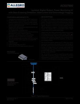
  • 1. TheAllegroACS37800 power monitoring IC greatly simplifies the addition of power monitoring to manyAC or DC powered systems. The sensor may be powered from the same supply as the system’s MCU, eliminating the need for multiple power supplies. The device’s construction includes a copper conduction path that generates a magnetic field proportional to applied current. The magnetic field is sensed differentially to reject errors introduced by common mode fields. Allegro’s Hall-effect-based, galvanically isolated current sensing technology achieves reinforced isolation ratings (4800 VRMS) in a small PCB footprint. These features enable isolated current sensing without expensive Rogowski coils, oversized current transformers, isolated operational amplifiers, or the power loss of shunt resistors. The ACS37800 power monitoring IC offers key power measurement parameters that can easily be accessed through its SPI or I2C digital protocol interfaces. Dedicated and configurable I/O pins for voltage/current zero crossing, undervoltage and overvoltage reporting, and fast overcurrent fault detection are available in I2C mode. User configuration of the IC is available through on-chip EEPROM. The ACS37800 is provided in a small low-profile surface mount SOIC16 wide-body package, is lead (Pb) free, and is fully calibrated prior to shipment from theAllegro factory. Customer calibration can further increase accuracy in application. ACS37800-DS, Rev. 3 MCO-0001004 • Accurate power monitoring for AC and DC applications • UL 60950-1 (ed. 2) and UL 62368-1 (ed. 1) certified for reinforced isolation up to 517 VRMS in a single package • Accurate measurements of active, reactive, and apparent power, as well as power factor • Separate RMS and instantaneous measurements for both voltage and current channels • Two programmable averaging blocks • 0.85 mΩ primary conductor resistance for low power loss and high inrush current withstand capability • Compatible with floating and non-floating GND • Dedicated voltage or current zero crossing pin • Fast, user-programmable overcurrent fault pin (5 µs typ.) • User-programmable undervoltage and overvoltage RMS thresholds • 1 kHz bandwidth • Current sensing range up to 90 A • Options for I2C or SPI digital interface protocols Isolated, Digital Output, Power Monitoring IC with Zero-Crossing Detection, Overcurrent and Overvoltage Flagging PACKAGE Figure 1: Typical Application FEATURES AND BENEFITS DESCRIPTION Not to scale ACS37800 IP IP+ IP+ IP+ IP+ VINP VINN IP- IP- IP- IP- VCC GND 1 2 3 4 5 6 7 8 16 15 14 13 12 11 10 9 L (N) N (L) 1 MΩ 1 MΩ 1 MΩ 1 MΩ RSENSE MCU VCC GND To User ( REINFORCED ISOLATION Linear Regulator ACS37800 SDA / MISO SCL / SCLK DIO_0 / MOSI DIO_1 / CS Isolated Power Single Output Supply , etc.) Flyback RPULLUP RPULLUP I2 C Only 16-pin SOICW (suffix MA) March 17, 2022 CB Certificate Number: US-32210-M1-UL US-36315-UL
  • 2. Isolated, Digital Output, Power Monitoring IC with Zero-Crossing Detection, Overcurrent and Overvoltage Flagging ACS37800 2 Allegro MicroSystems 955 Perimeter Road Manchester, NH 03103-3353 U.S.A. www.allegromicro.com SELECTION GUIDE Part Number VCC(typ) (V) IPR (A) Communication Protocol TA (°C) Packing [1] ACS37800KMACTR-015B5-SPI 5 ±15 SPI –40 to 125 Tape and reel, 1000 pieces per reel, 3000 pieces per box ACS37800KMACTR-030B3-SPI 3.3 ±30 ACS37800KMACTR-030B3-I2C 3.3 ±30 I2C ACS37800KMACTR-090B3-I2C 3.3 ±90 [1] Contact Allegro for additional packing options. ACS 37800 K MAC - 015 B 5 Supply Voltage: 5 – VCC = 5 V 3 – VCC = 3.3 V Output Directionality: B – Bidirectional Current Sensing Range (A) Package Designator Operating Temperature Range 5 Digit Part Number Allegro Current Sensor TR Packing Designator Communication Protocol - SPI
  • 3. Isolated, Digital Output, Power Monitoring IC with Zero-Crossing Detection, Overcurrent and Overvoltage Flagging ACS37800 3 Allegro MicroSystems 955 Perimeter Road Manchester, NH 03103-3353 U.S.A. www.allegromicro.com ISOLATION CHARACTERISTICS Characteristic Symbol Notes Rating Unit Dielectric Strength Test Voltage VISO Agency type-tested for 60 seconds per UL 60950-1 (edition 2) and UL 62368-1 (edition 1); Production tested at 3000 VRMS for 1 second, in accordance with UL 60950-1 (edition 2) and UL 62368-1 (edition 1) 4800 VRMS Working Voltage for Basic Isolation VWVBI Maximum approved working voltage for basic (single) isolation according to UL 60950-1 (edition 2) and UL 62368-1 (edition 1) 1480 VPK or VDC 1047 VRMS Working Voltage for Reinforced Isolation VWVRI Maximum approved working voltage for reinforced isolation according to UL 60950-1 (edition 2) and UL 62368-1 (edition 1) 730 VPK or VDC 517 VRMS Clearance Dcl Minimum distance through air from IP leads to signal leads 7.5 mm Creepage Dcr Minimum distance along package body from IP leads to signal leads 7.9 mm Distance Through Insulation DTI Minimum internal distance through insulation 90 μm Comparative Tracking Index CTI Material Group II 400 to 599 V ABSOLUTE MAXIMUM RATINGS Characteristic Symbol Notes Rating Units Supply Voltage VCC 6.5 V Reverse Supply Voltage VRCC –0.5 V Input Voltage VINP, VINN VCC + 0.5 V Reverse Input Voltage VRNP, VRNN –0.5 V Digital I/O Voltage VDIO SPI, I2C, and general purpose I/O 6 V Reverse Digital I/O Voltage VRDIO –0.5 V Maximum Continuous Current ICMAX TA = 25°C 60 A Operating Ambient Temperature TA Range K –40 to 125 °C Junction Temperature TJ(max) 165 °C Storage Temperature Tstg –65 to 170 °C THERMAL CHARACTERISTICS Characteristic Symbol Test Conditions [1] Value Units Package Thermal Resistance (Junction to Ambient) RθJA Mounted on the Allegro ASEK37800 evaluation board with 750 mm2 of 4 oz. copper on each side, connected to pins 1 and 2, and to pins 3 and 4, with thermal vias connecting the layers. Performance values include the power consumed by the PCB. 23 °C/W Package Thermal Resistance (Junction to Lead) RθJL Mounted on the Allegro ACS37800 evaluation board. 5 °C/W [1] Refer to the Thermal Performance section below. ESD RATINGS Characteristic Symbol Notes Value Unit Human Body Model VHBM Per JEDEC JS-001 ±5 kV Charged Device Model VCDM Per JEDEC JS-002 ±1 kV
  • 4. Isolated, Digital Output, Power Monitoring IC with Zero-Crossing Detection, Overcurrent and Overvoltage Flagging ACS37800 4 Allegro MicroSystems 955 Perimeter Road Manchester, NH 03103-3353 U.S.A. www.allegromicro.com FUNCTIONAL BLOCK DIAGRAM Bandgap Reference Fault Logic Temperature Sensor IP+ IP– VCC GND To All Subcircuits Hall Sensor Array Metrology Engine I2C/SPI Communication EEPROM + Charge Pump Temperature Compensation Logic DIGITAL SYSTEM VINN VINP ADC ADC SDA / MISO SCL / SCLK DIO_0 / MOSI DIO_1 / CS V I Terminal List Table Number Name Description I2C SPI 1, 2, 3, 4 IP+ Terminals for current being sensed; fused internally 5, 6, 7, 8 IP- Terminals for current being sensed; fused internally 9 DIO_1/CS Digital I/O 1 Chip Select (CS) 10 DIO_0/MOSI Digital I/O 0 MOSI 11 SCL  /SCLK SCL SCLK 12 SDA   /MISO SDA MISO 13 VCC Device power supply terminal 14 GND Device ground terminal 15 VINN Negative input voltage (always connect to GND) 16 VINP Positive input voltage Pinout Diagram 1 IP+ 2 IP+ 3 IP+ 4 IP+ 5 IP- 6 IP- 7 IP- 8 IP- 9 10 DIO_0 / MOSI 11 SCL / SCLK 12 SDA / MISO 13 VCC 14 GND 15 VINN 16 VINP DIO_1 / CS PINOUT DIAGRAM AND TERMINAL LIST Figure 2: Functional Block Diagram
  • 5. Isolated, Digital Output, Power Monitoring IC with Zero-Crossing Detection, Overcurrent and Overvoltage Flagging ACS37800 5 Allegro MicroSystems 955 Perimeter Road Manchester, NH 03103-3353 U.S.A. www.allegromicro.com Table of Contents Features and Benefits............................................................ 1 Description........................................................................... 1 Package.............................................................................. 1 Typical Application................................................................. 1 Selection Guide.................................................................... 2 Absolute Maximum Ratings.................................................... 3 Isolation Characteristics......................................................... 3 ESD Ratings......................................................................... 3 Thermal Characteristics......................................................... 3 Functional Block Diagram...................................................... 4 Pinout Diagram and Terminal List............................................ 4 Electrical Characteristics........................................................ 6 15B5 Performance Characteristics.......................................... 8 30B3 Performance Characteristics.......................................... 9 90B3 Performance Characteristics........................................ 10 I2C Operating Characteristics................................................11 SPI Operating Characteristics............................................... 12 Theory of Operation............................................................ 13 Introduction..................................................................... 13 Voltage and Current Measurements................................... 13 Overcurrent Measurement Path......................................... 13 Trim Methods.................................................................. 13 Power Calculations.......................................................... 14 Operational Block Diagram................................................... 15 Configurable Settings....................................................... 16 Configuring the DIO Pins (I2C Devices) ............................. 16 Configuring the Device for AC Applications............................. 19 Device EEPROM Settings................................................. 19 Voltage Measurement....................................................... 19 Current Measurement....................................................... 20 Configuring the Device for DC Applications............................ 21 Device EEPROM Settings................................................. 21 Voltage Measurement....................................................... 21 Current Measurement....................................................... 21 RMS and Power Accuracy vs. Operation Point........................ 21 RMS and Power Output Error vs. Applied Input.................... 21 15B5 IRMS and Power Error ............................................ 22 30B3 IRMS and Power Error ............................................ 22 90B3 IRMS and Power Error ............................................ 22 Digital Communication......................................................... 23 Communication Interfaces................................................. 23 SPI................................................................................. 23 Registers and EEPROM................................................... 23 EEPROM Error Checking and Correction (ECC).................. 25 I2C Slave Addressing........................................................ 25 EEPROM/Shadow Memory Map........................................... 26 Register Details – EEPROM.............................................. 27 Volatile Memory Map........................................................ 32 Register Details – Volatile................................................. 33 Application Information........................................................ 38 Thermal Rise vs. Primary Current...................................... 38 ASEK37800 Evaluation Board Layout................................. 38 Recommended PCB Layout................................................. 39 Package Outline Drawing..................................................... 40
  • 6. Isolated, Digital Output, Power Monitoring IC with Zero-Crossing Detection, Overcurrent and Overvoltage Flagging ACS37800 6 Allegro MicroSystems 955 Perimeter Road Manchester, NH 03103-3353 U.S.A. www.allegromicro.com Characteristic Symbol Test Conditions Min. Typ. Max. Unit ELECTRICAL CHARACTERISTICS Supply Voltage VCC 5 V variant 4.5 5 5.5 V 3.3 V variant 2.97 3.3 3.63 V Supply Current ICC VCC(min) ≤ VCC ≤ VCC(max), no load on output pins – 12 15 mA Supply Bypass Capacitor CBYPASS VCC to GND recommended 0.1 – – µF Power-On Time tPO – 90 – µs VOLTAGE INPUT BUFFER Differential Input Range ΔVINR ΔVIN = VINP – VINN(GND) –250 – 250 mV Dynamic Input Frequency fdyn_in bypass_n_en = 0 35 – 300 Hz VOLTAGE CHANNEL ADC Sample Frequency fS_V – 32 – kHz Number of Bits ADCV_B – 16 – bits ADC Fullscale ADCV_FS ΔVIN = ±250 mV, VINN= GND –27500 – 27500 codes Sensitivity Sens(V) ΔVINR(min) < ΔVIN < ΔVINR(max) – 110 – LSB / mV Voltage Channel Power Supply Error PSEV_O Ratio of change on VCC to change in offset at DC, 100% ±10% VCC(typ) –7 – 7 codes / %VCC PSEV_S Ratio of change on VCC to change in sensitivity at DC, 100% ±10% VCC(typ) –0.1 – 0.1 % / %VCC Voltage Channel Power Supply Rejection Ratio PSRRV_O Ratio of change on VCC to change in offset, 10 Hz to 10 kHz, 10% VCC(pk-pk) 60 70 – dB PSRRV_S Ratio of change on VCC to change in sensitivity, 10 Hz to 10 kHz, 10% VCC(pk-pk) 60 75 – dB VOLTAGE CHANNEL Internal Bandwidth BW – 1 – kHz RMS Noise NV Input referred – ±0.3 – mV Linearity Error ELIN_V – ±0.2 – % CURRENT CHANNEL Sample Frequency fS_C – 32 – kHz Number of Bits ADCI_B – 16 – bits ADC Fullscale ADCI_FS IP = IPR(min) or IPR(max) –27500 – 27500 codes Current Channel Power Supply Error PSEI_O Ratio of change on VCC to change in offset at DC, 100% ±10% VCC(typ) –60 – 60 codes / %VCC PSEI_S Ratio of change on VCC to change in sensitivity at DC, 100% ±10% VCC(typ) –0.3 – 0.3 % / %VCC Current Channel Power Supply Rejection Ratio PSRRI_O Ratio of change on VCC to change in offset, 10 Hz to 10 kHz, 10% VCC(pk-pk) 60 65 – dB PSRRI_S Ratio of change on VCC to change in sensitivity, 10 Hz to 10 kHz, 10% VCC(pk-pk) 20 40 – dB Internal Bandwidth BW – 1 – kHz Primary Conductor Resistance RIP TA = 25°C – 0.85 – mΩ Continued on next page... COMMON ELECTRICAL CHARACTERISTICS [1]: Valid through the full range of TA and VCC = VCC(typ), unless otherwise specified
  • 7. Isolated, Digital Output, Power Monitoring IC with Zero-Crossing Detection, Overcurrent and Overvoltage Flagging ACS37800 7 Allegro MicroSystems 955 Perimeter Road Manchester, NH 03103-3353 U.S.A. www.allegromicro.com Characteristic Symbol Test Conditions Min. Typ. Max. Unit CURRENT CHANNEL (continued) RMS Noise NI Input referred – ±0.1 – A Linearity Error ELIN_I – ±1.5 – % OVERCURRENT FAULT CHARACTERISTICS Fault Response Time tRF Time from IP rising above IFAULT until VFAULT < VFAULT(max) for a current step from 0 to 1.2 × IFAULT; 10 kΩ and 100 pF from DIO_1 to ground; fltdly = 0 – 5 – μs Internal Bandwidth BW – 200 – kHz Fault Hysteresis [2] IHYST – 0.06 × FS – A Fault Range IFAULT Set using fault field in EEPROM 0.65 × FS – 2.00 × FS A VOLTAGE ZERO CROSSING Voltage Zero-Crossing Delay td – 250 – µs DIO PINS DIO Output High Level VOH(DIO) VCC = 3.3 V 3 – – V DIO Output Low Level VOL(DIO) VCC = 3.3 V – – 0.3 V DIO Input Voltage for Address Selection 0 VADD0 VCC = 3.3 V – 0 – V DIO Input Voltage for Address Selection 1 VADD1 VCC = 3.3 V – 1.1 – V DIO Input Voltage for Address Selection 2 VADD2 VCC = 3.3 V – 2.2 – V DIO Input Voltage for Address Selection 3 VADD3 VCC = 3.3 V – 3.3 – V [1] Device may be operated at higher primary current levels (IP), ambient temperatures (TA), and internal leadframe temperatures, provided that the maximum junction temperature (TJ(max)) is not exceeded. [2] After IP goes above IFAULT, tripping the internal fault comparator, IP must go below IFAULT – IHYST before the internal fault comparator will reset. COMMON ELECTRICAL CHARACTERISTICS [1] (continued): Valid through the full range of TA and VCC = VCC(typ), unless otherwise specified
  • 8. Isolated, Digital Output, Power Monitoring IC with Zero-Crossing Detection, Overcurrent and Overvoltage Flagging ACS37800 8 Allegro MicroSystems 955 Perimeter Road Manchester, NH 03103-3353 U.S.A. www.allegromicro.com Characteristic Symbol Test Conditions Min. Typ. [1] Max. Unit GENERAL CHARACTERISTICS Nominal Supply Voltage VCC(typ) – 5 – V NOMINAL PERFORMANCE – FACTORY CURRENT CHANNEL Current Sensing Range IPR –15 – 15 A Sensitivity Sens(I) IPR(min) < IP < IPR(max) – 1833.3 – LSB/A NOMINAL PERFORMANCE – INPUT REFERRED FACTORY POWER (POWER SEEN BY THE DEVICE) [2] Active Power Sensitivity SensPd_act – 6.15 – LSB/mW Imaginary Power Sensitivity SensPd_img – 12.31 – LSB/mVAR Apparent Power Sensitivity SensPd_app – 12.31 – LSB/mVA TOTAL OUTPUT ERROR COMPONENTS [3] – CURRENT CHANNEL Sensitivity Error ESENS(I) Measured at IP = IPR(max), TA = 25°C to 125°C – ±1.1 – % Measured at IP = IPR(max), TA = –40°C to 25°C – ±1.5 – % Offset Error EO(I) IP = 0 A, TA = 25°C to 125°C – ±720 – LSB IP = 0 A, TA = –40°C to 25°C – ±780 – LSB Total Output Error ETOT(I) Measured at IP = IPR(max), TA = 25°C to 125°C – ±2.1 – % Measured at IP = IPR(max), TA = –40°C to 25°C – ±2.7 – % TOTAL OUTPUT ERROR COMPONENTS [3] – VOLTAGE CHANNEL Sensitivity Error ESENS(V) Measured at ΔVIN = ΔVINR(max), TA = 25°C to 125°C – ±1.2 – % Measured at ΔVIN = ΔVINR(max), TA = –40°C to 25°C – ±1.2 – % Offset Error EO(V) ΔVIN = 0 mV, TA = 25°C to 125°C – ±55 – LSB ΔVIN = 0 mV, TA = –40°C to 25°C – ±55 – LSB Total Output Error ETOT(V) Measured at ΔVIN = ΔVINR(max), TA = 25°C to 125°C – ±1.4 – % Measured at ΔVIN = ΔVINR(max), TA = –40°C to 25°C – ±1.4 – % ACCURACY PERFORMANCE – ACTIVE POWER Total Output Error ETOT(P) IP = IPR(max), measured at ΔVIN = ΔVINR(max), TA = 25°C to 125°C – ±2.1 – % IP = IPR(max), measured at ΔVIN = ΔVINR(max), TA = –40°C to 25°C – ±3 – % [1] Typical values are mean ±3 sigma. [2] These sensitivity characteristics are referred to the inputs seen by the device, i.e. the voltage channel resistor divider must be accounted to determine the system sensi- tivies. [3] ETOT = ESENS + 100 x VOE/(Sens x IP) ACS37800KMAC-015B5 PERFORMANCE CHARACTERISTICS: Valid through the full operating temperature range, TA = –40°C to 125°C, CBYPASS = 0.1 µF, and VCC = 5 V, unless otherwise specified
  • 9. Isolated, Digital Output, Power Monitoring IC with Zero-Crossing Detection, Overcurrent and Overvoltage Flagging ACS37800 9 Allegro MicroSystems 955 Perimeter Road Manchester, NH 03103-3353 U.S.A. www.allegromicro.com Characteristic Symbol Test Conditions Min. Typ. [1] Max. Unit GENERAL CHARACTERISTICS Nominal Supply Voltage VCC(typ) – 3.3 – V NOMINAL PERFORMANCE – CURRENT CHANNEL Current Sensing Range IPR –30 – 30 A Sensitivity Sens(I) IPR(min) < IP < IPR(max) – 916.7 – LSB/A NOMINAL PERFORMANCE – INPUT REFERRED FACTORY POWER (POWER SEEN BY THE DEVICE) [2] Active Power Sensitivity SensPd_act – 3.08 – LSB/mW Imaginary Power Sensitivity SensPd_img – 6.15 – LSB/mVAR Apparent Power Sensitivity SensPd_app – 6.15 – LSB/mVA TOTAL OUTPUT ERROR COMPONENTS [3] – CURRENT CHANNEL Sensitivity Error ESENS(I) Measured at IP = IPR(max), TA = 25°C to 125°C – ±1 – % Measured at IP = IPR(max), TA = –40°C to 25°C – ±1.5 – % Offset Error EO(I) IP = 0 A, TA = 25°C to 125°C – ±510 – LSB IP = 0 A, TA = –40°C to 25°C – ±570 – LSB Total Output Error ETOT(I) Measured at IP = IPR(max), TA = 25°C to 125°C – ±2 – % Measured at IP = IPR(max), TA = –40°C to 25°C – ±2.7 – % TOTAL OUTPUT ERROR COMPONENTS [3] – VOLTAGE CHANNEL Sensitivity Error ESENS(V) Measured at ΔVIN = ΔVINR(max), TA = 25°C to 125°C – ±0.75 – % Measured at ΔVIN = ΔVINR(max), TA = –40°C to 25°C – ±0.75 – % Offset Error EO(V) ΔVIN = 0 mV, TA = 25°C to 125°C – ±55 – LSB ΔVIN = 0 mV, TA = –40°C to 25°C – ±55 – LSB Total Output Error ETOT(V) Measured at ΔVIN = ΔVINR(max), TA = 25°C to 125°C – ±1 – % Measured at ΔVIN = ΔVINR(max), TA = –40°C to 25°C – ±1 – % ACCURACY PERFORMANCE – ACTIVE POWER Total Output Error ETOT(P) IP = IPR(max), measured at ΔVIN = ΔVINR(max), TA = 25°C to 125°C – ±2.1 – % IP = IPR(max), measured at ΔVIN = ΔVINR(max), TA = –40°C to 25°C – ±3 – % [1] Typical values are mean ±3 sigma. [2] These sensitivity characteristics are referred to the inputs seen by the device, i.e. the voltage channel resistor divider must be accounted to determine the system sensi- tivies. [3] ETOT = ESENS + 100 x VOE/(Sens x IP) ACS37800KMAC-030B3 PERFORMANCE CHARACTERISTICS: Valid through the full operating temperature range, TA = –40°C to 125°C, CBYPASS = 0.1 µF, and VCC = 3.3 V, unless otherwise specified
  • 10. Isolated, Digital Output, Power Monitoring IC with Zero-Crossing Detection, Overcurrent and Overvoltage Flagging ACS37800 10 Allegro MicroSystems 955 Perimeter Road Manchester, NH 03103-3353 U.S.A. www.allegromicro.com Characteristic Symbol Test Conditions Min. Typ. [1] Max. Unit GENERAL CHARACTERISTICS Nominal Supply Voltage VCC(typ) – 3.3 – V NOMINAL PERFORMANCE – CURRENT CHANNEL Current Sensing Range IPR –90 – 90 A Sensitivity Sens(I) IPR(min) < IP < IPR(max) – 305.6 – LSB/A NOMINAL PERFORMANCE – INPUT REFERRED FACTORY POWER (POWER SEEN BY THE DEVICE) [2] Active Power Sensitivity SensPd_act – 1.03 – LSB/mW Imaginary Power Sensitivity SensPd_img – 2.05 – LSB/mVAR Apparent Power Sensitivity SensPd_app – 2.05 – LSB/mVA TOTAL OUTPUT ERROR COMPONENTS [3] – CURRENT CHANNEL Sensitivity Error ESENS(I) Measured at IP = IPR(max), TA = 25°C to 125°C – ±1 – % Measured at IP = IPR(max), TA = –40°C to 25°C – ±1.5 – % Offset Error EO(I) IP = 0 A, TA = 25°C to 125°C – ±180 – LSB IP = 0 A, TA = –40°C to 25°C – ±210 – LSB Total Output Error ETOT(I) Measured at IP = 45 A, TA = 25°C to 125°C – ±2 – % Measured at IP = 45 A, TA = –40°C to 25°C – ±2.6 – % TOTAL OUTPUT ERROR COMPONENTS [3] – VOLTAGE CHANNEL Sensitivity Error ESENS(V) Measured at ΔVIN = ΔVINR(max), TA = 25°C to 125°C – ±0.75 – % Measured at ΔVIN = ΔVINR(max), TA = –40°C to 25°C – ±0.75 – % Offset Error EO(V) ΔVIN = 0 mV, TA = 25°C to 125°C – ±55 – LSB ΔVIN = 0 mV, TA = –40°C to 25°C – ±55 – LSB Total Output Error ETOT(V) Measured at ΔVIN = ΔVINR(max), TA = 25°C to 125°C – ±1 – % Measured at ΔVIN = ΔVINR(max), TA = –40°C to 25°C – ±1 – % ACCURACY PERFORMANCE – ACTIVE POWER Total Output Error ETOT(P) IP = 45 A, measured at ΔVIN = ΔVINR(max), TA = 25°C to 125°C – ±1.3 – % IP = 45 A, measured at ΔVIN = ΔVINR(max), TA = –40°C to 25°C – ±2.1 – % [1] Typical values are mean ±3 sigma. [2] These sensitivity characteristics are referred to the inputs seen by the device, i.e. the voltage channel resistor divider must be accounted to determine the system sensi- tivies. [3] ETOT = ESENS + 100 x VOE/(Sens x IP) ACS37800KMAC-090B3 PERFORMANCE CHARACTERISTICS: Valid through the full operating temperature range, TA = –40°C to 125°C, CBYPASS = 0.1 µF, and VCC = 3.3 V, unless otherwise specified
  • 11. Isolated, Digital Output, Power Monitoring IC with Zero-Crossing Detection, Overcurrent and Overvoltage Flagging ACS37800 11 Allegro MicroSystems 955 Perimeter Road Manchester, NH 03103-3353 U.S.A. www.allegromicro.com Characteristic Symbol Test Conditions Min. Typ. Max. Unit I2C INTERFACE CHARACTERISTICS [2] Bus Free Time Between Stop and Start tBUF 1.3 – – µs Hold Time Start Condition thdSTA 0.6 – – µs Setup Time for Repeated Start Condition tsuSTA 0.6 – – µs SCL Low Time tLOW 1.3 – – µs SCL High Time tHIGH 0.6 – – µs Data Setup Time tsuDAT 100 – – µs Data Hold Time thdDAT 0 – 900 µs Setup Time for Stop Condition tsuSTO 0.6 – – µs Logic Input Low Level (SDA, SCL pins) VIL – – 30 %VCC Logic Input High Level (SDA, SCL pins) VIH 70 – – %VCC Logic Input Current IIN Input voltage on SDA or SCL = 0 V to VCC –1 – 1 µA Output Low Voltage (SDA) VOL SDA sinking = 1.5 mA – – 0.36 V Clock Frequency (SCL pin) fCLK – – 400 kHz Output Fall Time (SDA pin) tf REXT = 2.4 kΩ, CB = 100 pF – – 250 ns I2C Pull-Up Resistance REXT 2.4 10 – kΩ Total Capacitive Load for Each of SDA and SCL Buses CB – – 20 pF [1] Validated by characterization and design. [2] These values are ratiometric to the supply voltage. I2C Interface Characteristics are ensured by design and not factory tested. xKMACTR-I2C OPERATING CHARACTERISTICS [1]: Valid through the full range of TA, VCC = VCC(typ), REXT = 10 kΩ, unless otherwise specified tsuSTA tsuDAT tLOW tsuSTO thdSTA thdDAT tHIGH tBUF SDA SCL Figure 3: I2C Interface Timing
  • 12. Isolated, Digital Output, Power Monitoring IC with Zero-Crossing Detection, Overcurrent and Overvoltage Flagging ACS37800 12 Allegro MicroSystems 955 Perimeter Road Manchester, NH 03103-3353 U.S.A. www.allegromicro.com Characteristic Symbol Test Conditions Min. Typ. Max. Unit SPI INTERFACE CHARACTERISTICS Digital Input High Voltage VIH MOSI, SCLK, CS pins, VCC = 3.3 V 2.8 – 3.63 V MOSI, SCLK, CS pins, VCC = 5 V 4 – 5.5 V Digital Input Low Voltage VIL MOSI, SCLK, CS pins – – 0.5 V SPI Output High Voltage VOH MISO pin, CL = 20 pF, TA = 25°C, VCC(typ) = 3.3 V 2.8 3.3 3.8 V MISO pin, CL = 20 pF, TA = 25°C, VCC(typ) = 5 V 4 5 5.5 V SPI Output Low Voltage VOL MISO pin, CL = 20 pF, TA = 25°C – 0.3 0.5 V SPI Clock Frequency fSCLK MISO pin, CL = 20 pF 0.1 – 10 MHz SPI Frame Rate tSPI 5.8 – 588 kHz Chip Select to First SCLK Edge tCS Time from CS going low to SCLK falling edge 50 – – ns Data Output Valid Time tDAV Data output valid after SCLK falling edge – 40 – ns MOSI Setup Time tSU Input setup time before SCLK rising edge 25 – – ns MOSI Hold Time tHD Input hold time after SCLK rising edge 50 – – ns SCLK to CS Hold Time tCHD Hold SCLK high time before CS rising edge 5 – – ns Load Capacitance CL Loading on digital output (MISO) pin – – 20 pF [1] Validated by characterization and design. xKMATR-SPI OPERATING CHARACTERISTICS [1]: Valid through the full range of TA, VCC = VCC(typ), unless otherwise specified CSN SCLK MOSI MISO tCS tSU tHD tDAV tCHD >tCS Figure 4: SPI Timing
  • 13. Isolated, Digital Output, Power Monitoring IC with Zero-Crossing Detection, Overcurrent and Overvoltage Flagging ACS37800 13 Allegro MicroSystems 955 Perimeter Road Manchester, NH 03103-3353 U.S.A. www.allegromicro.com THEORY OF OPERATION Introduction The ACS37800 provides a simple solution for voltage, current, and power monitoring in 60 Hz AC and DC applications and is particularly well suited for high isolation. The voltage is mea- sured by resistor dividing it down to fit the input range of the on-board voltage sense amplifier, as well as to add isolation. The current is measured using the integrated current loop and galvanically isolated Hall sensor. Both analog signals are then sampled using high accuracy ADCs before entering the digital system. Here, the metrology engine is used to determine fre- quency, calculate RMS values of current, voltage, and power, as well as provide a range of averaging and configuration options. One can choose to read out all the different information provided using SPI or I2C. When using I2C, there are also options for using some of the digital I/O pins for overcurrent or zero cross- ing detection. Overall, with a high degree of configurability and integrated features, the ACS37800 can fit most power monitoring applications. The following sections will help explain in more detail these features and configuration options, as well as how to best use the ACS37800 for particular applications. Voltage and Current Measurements The main signal paths for the current and voltage measurement, through the ADCs and internal filtering, have a bandwidth of 1 kHz and an update rate of 32 kHz. These “instantaneous” current and voltage measurements are stored in the icodes and vcodes fields. The instantaneous apparent power, which is the product of icodes and vcodes, is stored in the field pinstant. Overcurrent Measurement Path A separate filter on the current ADC is used to create a lower resolution but higher bandwidth sample rate measurement of the current to be used for overcurrent detection. This filter outputs a 12-bit word at a 1 MHz update rate and 200 kHz bandwidth. The overcurrent fault logic compares this auxiliary current value to the user-defined overcurrent fault threshold, defined by the field fault. It is important to note that the trim for the main 16-bit current path is also applied to the overcurrent path, such that the overcurrent fault has the same level of accuracy as the main signal path. Trim Methods The trim logic for the voltage and current channels is depicted in Figure 5 and Figure 6. Refer to the Register Details section for more information regarding trim fields. In general, each chan- nel, voltage and current, is trimmed for gain and offset both at room and over temperature. This trim is done before the icodes and vcodes registers. The user has the ability to trim the nominal room temperature value. Figure 5: Voltage Channel Trim Flow Figure 6: Current Channel Trim Flow Delay Z-x chan_del_sel ichan_del_en Satura�on Gain Trim VchanGainSel Offset Trim + + + + vchan_offset_code vqvo_tc vcodes adc_out_v Factory Trim Satura�on Gain Trim sns_fine sns_tc Offset Trim + + + + qvo_fine qvo_tc Delay Z-x chan_del_sel ichan_del_en icodes adc_out_i Factory Trim
  • 14. Isolated, Digital Output, Power Monitoring IC with Zero-Crossing Detection, Overcurrent and Overvoltage Flagging ACS37800 14 Allegro MicroSystems 955 Perimeter Road Manchester, NH 03103-3353 U.S.A. www.allegromicro.com Power Calculations VOLTAGE ZERO CROSSING The RMS and power calculations of the ACS37800 are calcu- lated over a window of N samples. By default, this window is calculated dynamically based on the zero crossings of the voltage signal. A rising voltage zero crossing triggers the start of a new window. N then increases with each 32 kHz sample until the next rising voltage zero crossing, recording the current and voltage readings at each sample. This ends the calculation window, and all RMS and power calculations are performed on the saved data. During this time, the next calculation window is started. Voltage zero crossings are detected with time-based hysteresis that removes the possibility of noise causing multiple zero cross- ings to be reported at each true zero crossing. IRMS AND VRMS The cycle-by-cycle calculation of the root mean square of both the current and voltage channels is: IRMS = ∑ N n = N – 1 n = 0 In 2 VRMS = ∑ N n = N – 1 n = 0 Vn 2 where In (icodes) and Vn (vcodes) are the instantaneous measure- ments of current and voltage, respectively. APPARENT POWER The magnitude of the complex power being measured; calculated at the end of each cycle is: |S| = IRMS × VRMS ACTIVE POWER The real component of power being measured, calculated cycle by cycle is: PACTIVE = ∑ N n = N – 1 n = 0 Pn Pn = In × Vn REACTIVE POWER The imaginary component of power being measured, calculated at the end of each cycle is: Q = S2 – PACTIVE 2 POWER FACTOR The magnitude of the ratio of the real power to apparent power, calculated at the end of each cycle is: |PF| = |S| PACTIVE LEADING OR LAGGING POWER FACTOR The current leading or lagging the voltage is communicated as a single bit, posangle. This bit represents the sign of the reactive power. The sign of the reactive power is determined by compar- ing the timing of the zero crossings of the current and voltage. As such, it is only meaningful in the case of a linear load. The sign of the reactive power, posangle, along with the sign of the power factor, pospf, can be used to determine whether the load is inductive or capacitive, as well as whether power is being generated or consumed. This is shown in the four-quadrant figure below (refer to Figure 7). Imaginary Real POSPF = 1 POSANG = 1 POSPF = 0 POSANG = 0 POSPF = 0 POSANG = 1 POSPF = 1 POSANG = 0 Lagging Leading Capacitive and Generating Capacitive and Consuming Inductive and Consuming Inductive and Generating Figure 7: Four Quadrant, Power Factor Figure 8: Power Triangle Apparent Power, S = VI Active Power, P = VI cosФ Reactive Power, Q = VI sinФ Ф S = P 2 + Q 2
  • 15. Isolated, Digital Output, Power Monitoring IC with Zero-Crossing Detection, Overcurrent and Overvoltage Flagging ACS37800 15 Allegro MicroSystems 955 Perimeter Road Manchester, NH 03103-3353 U.S.A. www.allegromicro.com Factory Trimmed Current ADC RSENSE ΣRISO + RSENSE VLINE Voltage ADC Temperature Compensation Digital Filter Voltage Zero Crossing vrms papparent irms ovrms uvrms pinstant pactive pimag Averaging vrmsavgonesec vrmsavgonemin irmsavgonemin irmsavgonesec pactiveavgonesec pactiveavgonemin 0 1 0 1 iavgselen pavgselen RMS and Power Calculations O/UVRMS Flag Channel Delay Control icodes vcodes X icodes vcodes Zero Crossing Flag vrms irms pactive Voltage and Current Measurement RMS, and Power Calculation Averaging and VRMS Flagging IP+ IP– Overcurrent Fault Comparator fault fault out Register Voltage data Current data Power data Control Output Operation FAULT data pospf posangle OPERATIONAL BLOCK DIAGRAM Figure 9: Operational Block Diagram
  • 16. Isolated, Digital Output, Power Monitoring IC with Zero-Crossing Detection, Overcurrent and Overvoltage Flagging ACS37800 16 Allegro MicroSystems 955 Perimeter Road Manchester, NH 03103-3353 U.S.A. www.allegromicro.com Configurable Settings PHASE DELAY Phase delay may be introduced on either the voltage or current channel to account for known phase delay at other points in the system using the ichan_del_en and chan_ del_sel fields. ichan_ del_en determines if the voltage channel or current channel will be delayed. The chosen channel will be delayed by the configured amount in chan_del_sel, up to 5° of delay. AVERAGING CHANNEL The ACS37800 contains two averaging paths. VRMS, IRMS, and PACTIVE can be routed to these average blocks as shown in Figure 9 using iavgselen and pavgselen. AVERAGING TIME Each averaging path on the ACS37800 consists of two averag- ing blocks that each allow for a configurable number of averages based on the EEPROM fields rms_avg_1 and rms_avg_2. The output of the first averaging block feeds into the input of the second averaging block. The output of each block is accessible for each channel. OVERVOLTAGE AND UNDERVOLTAGE DETECTION FOR VRMS This device has programmable overvoltage and undervoltage RMS flags that will signal when the vrms is above or below the respective thresholds. The vrms is compared to the overvoltage and undervoltage RMS thresholds set by the fields overvreg and undervreg to determine a flag condition. The number of suc- cessive sample sets required to trigger either the overvoltage or undervoltage RMS flag can be set by the vevent_cycs field. The ovrms and uvrms flags can be routed to the DIO pins when the device is used in I2C mode. See Configuring the DIO Pins. OVERCURRRENT DETECTION FOR INSTANTA- NEOUS CURRENT The overcurrent fault threshold may be set from 0.65 × IPR to 2.0 × IPR. The user sets the trip point with the field fault. The user can add a digital delay to the overcurrent fault with the field flt_dly. Up to 32 µs delay can be added to the overcurrent fault. BYPASSING THE DYNAMIC FRAMING OF THE RMS CALCULATION WINDOW By default, the ACS37800 dynamically calculates the value of N to be used in the RMS and power calculations based on the zero crossings on the voltage channel. This functionality can be disabled using the bypass_n_en field. When bypass_n_en = 1, it is important to define the number of samples used to calculate RMS. This can be done in the field n. The field n is the number of 32 kHz samples that are used to calculate the RMS. The minimum effective n that is used when calculating RMS is 4. If a value of less than 4 is chosen for n, then 4 is internally used. The first useable RMS calculation on start up with bypass_n_en = 1 is after 2 × n samples. Configuring the DIO Pins (I2C Devices) FLAGS TO BE ROUTED TO THE DIO PINS When the device is configured to be in I2C mode (comm_sel in EEPROM = 1), pins 9 and 10 become digital I/O pins, DIO_1 and DIO_0, respectively. The digital I/O pins are low true, mean- ing that a voltage below the DIO Output Low Level maximum (VOL(DIO)max) is to be interpreted as logic 1 and a voltage above DIO Output High Level minimum (VOH(DIO)min) is to be inter- preted as a logic 0. The Digital I/O pins can be configured in EEPROM to represent the following functions: DIO_O dio_0_sel value (EEPROM) Function 0 ZC: zero crossing 1 ovrms: the VRMS overvoltage flag 2 uvrms: The VRMS undervoltage flag 3 The OR of ovrms and uvrms (if either flag is triggered, the DIO_0 pin will be asserted) OVRMS UVRMS OVRMS UVRMS OCF_LAT OCF ZC DIO_0 DIO_1 CS MOSI DIO_1 / CS DIO_0 / MOSI DIO_0_Sel[0..1] Comm_Sel DIO_1_Sel[0..1] Comm_Sel DIO_1 dio_1_sel value (EEPROM) Function 0 OCF: Overcurrent fault 1 uvrms: The VRMS undervoltage flag 2 ovrms: The VRMS overvoltage flag 3 The OR of ovrms and uvrms, and OCF_LAT [Latched Overcurrent Fault] (if any of the three flags are triggered, the DIO_1 pin will be asserted) OVRMS UVRMS OVRMS UVRMS OCF_LAT OCF ZC DIO_0 DIO_1 CS MOSI DIO_1 / CS DIO_0 / MOSI DIO_0_Sel[0..1] Comm_Sel DIO_1_Sel[0..1] Comm_Sel
  • 17. Isolated, Digital Output, Power Monitoring IC with Zero-Crossing Detection, Overcurrent and Overvoltage Flagging ACS37800 17 Allegro MicroSystems 955 Perimeter Road Manchester, NH 03103-3353 U.S.A. www.allegromicro.com ZERO CROSSING OUTPUT CONFIGURATIONS The dynamic calculation of N for the RMS and power calcula- tions uses exclusively the voltage zero crossing, but both current and voltage zero crossing can be flagged and reported on the DIO pins. Voltage Zero Crossing (VZC) The voltage zero crossing has two basic modes of operation, pulse mode and square wave mode. Pulse Mode – VZC In pulse mode, a voltage zero crossing is reported as a short pulse. There are three available configurations to customize the voltage zero crossing pulse mode operation: rising or falling edge selection, every edge selection, and pulse width. Rising Edge or Falling Edge Aligned Pulse The EEPROM field zerocrossedgesel is used to select whether the zero crossing output pulses are aligned to the rising zero crossing of the voltage channel or the falling zero crossing of the voltage channel. Figure 10: zerocrossedgesel = 0, Falling Zero Crossing Figure 11: zerocrossedgesel = 1, Rising Zero Crossing Pulse Every Edge The EEPROM field halfcycle_en is used to output a pulse at every zero crossing. Figure 12: halfcycle_en = 1, Both Rising and Falling Zero Crossings Signaled Pulse Width Selection The EEPROM field delaycnt_sel is used to select the width of the voltage zero crossing pulse. Table 1: delaycnt_sel Range Value Units 0 32 µs 1 256 µs
  • 18. Isolated, Digital Output, Power Monitoring IC with Zero-Crossing Detection, Overcurrent and Overvoltage Flagging ACS37800 18 Allegro MicroSystems 955 Perimeter Road Manchester, NH 03103-3353 U.S.A. www.allegromicro.com Square Wave Mode Square wave mode can be configured using the EEPROM field squarewave_en. In square wave mode, a voltage zero crossing is reported as a square wave that changes state on each reported zero crossing. The zerocrossedgesel EEPROM field can be used to align the low to high transition of the flag with either the rising voltage zero crossing or the falling voltage zero crossing. Figure 13: zerocrossedgesel = 0, Square Wave Mode Figure 14: zerocrossedgesel = 1, Square Wave Mode Current Zero Crossing (CZC) The current zero crossing function can be enabled using the EEPROM field zerocrosschansel. When the zero crossing flag is configured to flag zero crossings of the current path, this has no effect on the RMS and power calculations; the voltage zero crossing is still used for these calculations. The current zero crossing has just one basic mode of operation: pulse mode. Pulse Mode – CZC In pulse mode, a current zero crossing is reported as a short pulse. There are three available configurations to customize the current zero crossing pulse mode operation: rising or falling edge selection, every edge selection, and pulse width. Rising Edge or Falling Edge Aligned Pulse The EEPROM field zerocrossedgesel is used to select whether the zero crossing output pulses are aligned to the rising zero crossing of the current channel or the falling zero crossing of the current channel. Figure 15: zerocrossedgesel = 0, Falling Zero Crossing Figure 16: zerocrossedgesel = 1, Rising Zero crossing
  • 19. Isolated, Digital Output, Power Monitoring IC with Zero-Crossing Detection, Overcurrent and Overvoltage Flagging ACS37800 19 Allegro MicroSystems 955 Perimeter Road Manchester, NH 03103-3353 U.S.A. www.allegromicro.com Pulse Every Edge The EEPROM field halfcycle_en is used to output a pulse at every zero crossing. Figure 17: halfcycle_en = 1, Both Rising and Falling Zero Crossings Signaled CONFIGURING THE DEVICE FOR AC APPLICATIONS Device EEPROM Settings For AC power monitoring applications using the ACS37800, the following device settings are recommended: DYNAMIC CALCULATION OF N Set bypass_n_en = 0 (default). This setting enables the device to dynamically calculate N based off the voltage zero crossings. See the Register Details – EEPROM section for additional details. Voltage Measurement RECOMMENDED APPLICATION CIRCUITS An important aspect to consider when designing in the ACS37800 into AC applications is the design of the voltage mea- surement path. Typically, a resistor divider network is employed to provide both isolation and transform the high voltage signal into the ±250 mV signal that the ACS37800 can measure. There are two basic application circuits recommended based on the isolation requirements of the system. The first, see Figure 18, is to be used when the ACS37800 GND and the neutral terminal of the voltage input are connected. RISO1, RISO2, and RSENSE form a resistor divider network where, 𝑉𝑉𝐼𝐼𝐼𝐼 = 𝑉𝑉𝐿𝐿𝐿𝐿𝐿𝐿𝐿𝐿 ∗ 𝑅𝑅𝑆𝑆𝑆𝑆𝑆𝑆𝑆𝑆𝑆𝑆 𝑅𝑅𝐼𝐼𝐼𝐼𝐼𝐼1 + 𝑅𝑅𝐼𝐼𝐼𝐼𝐼𝐼2 + 𝑅𝑅𝑆𝑆𝑆𝑆𝑆𝑆𝑆𝑆𝑆𝑆 RISO1 and RISO2 should be equal. A value of 1 MΩ is appropriate for many applications, but ultimately, the resistance value used needs to comply with the required isolation of the system. RISO 1 1 MΩ 1 MΩ RISO 2 RSENSE VINP VINN Vin Figure 18: Voltage Channel Application Circuit; Device GND is Connected to Neutral
  • 20. Isolated, Digital Output, Power Monitoring IC with Zero-Crossing Detection, Overcurrent and Overvoltage Flagging ACS37800 20 Allegro MicroSystems 955 Perimeter Road Manchester, NH 03103-3353 U.S.A. www.allegromicro.com Another application circuit recommendation for the voltage chan- nel is shown in Figure 19. This is to be used in systems where the ACS37800 GND and the neutral terminal of the voltage input are to be isolated. Here, RISO3 and RISO4 are added to the resistor divider network. 𝑉𝑉𝐼𝐼𝐼𝐼 = 𝑉𝑉𝐿𝐿𝐿𝐿𝐿𝐿𝐿𝐿 ∗ 𝑅𝑅𝑆𝑆𝑆𝑆𝑆𝑆𝑆𝑆𝑆𝑆 𝑅𝑅𝐼𝐼𝐼𝐼𝐼𝐼1 + 𝑅𝑅𝐼𝐼𝐼𝐼𝐼𝐼2 + 𝑅𝑅𝐼𝐼𝐼𝐼𝐼𝐼3 + 𝑅𝑅𝐼𝐼𝐼𝐼𝐼𝐼4 + 𝑅𝑅𝑆𝑆𝑆𝑆𝑆𝑆𝑆𝑆𝑆𝑆 RISO1, RISO2, RISO3, and RISO4 should be equal and their value is determined by the isolation requirements of the system. A value of 1 MΩ is appropriate for many applications, but ultimately, the resistance value used needs to comply with the required isolation of the system. RISO 1 1 MΩ 1 MΩ 1 MΩ 1 MΩ RISO 2 RISO 3 RISO 4 RSENSE VINP VINN Vin Figure 19: Voltage Channel Application; Device GND is Isolated from Neutral To determine the value of RSENSE required for a particular appli- cation using either of the recommended circuits, the following equation can be used: 𝑅𝑅𝑆𝑆𝑆𝑆𝑆𝑆𝑆𝑆𝑆𝑆 = ∆𝑉𝑉𝐼𝐼𝐼𝐼𝐼𝐼(𝑀𝑀𝑀𝑀𝑀𝑀) 𝑉𝑉𝐿𝐿𝐿𝐿𝐿𝐿𝐿𝐿(𝑀𝑀𝑀𝑀𝑀𝑀) − ∆𝑉𝑉𝐼𝐼𝐼𝐼𝐼𝐼(𝑀𝑀𝑀𝑀𝑀𝑀) ∗ 𝑅𝑅𝐼𝐼𝐼𝐼𝐼𝐼 Where ΔVINR(MAX) = 250 mV, VLINE(MAX) is the maximum VLINE voltage to be measured, and RISO is the sum of all of the isolation resistors. If using the overvoltage detection functionality of the ACS37800, this should be considering when determining the maximum VLINE voltage to be measured. For example, in an application when the nominal VLINE is equal to 120 VRMS and a 50% over-voltage detection is required, VLINE(MAX) is: 120 VRMS × √2 × 1.5 = 255 V, where the √2 is used to approximate the peak voltage assuming a sinusoidal input. Additionally, the tolerance of the all resistors should be consid- ered when determining RSENSE. The minimum tolerance of the isolation resistors should be used along with the maximum toler- ance of RSENSE. If the RSENSE is not sized appropriately, this can lead to the voltage input to the ACS38700 exceeding the maximum input range, which can cause the instantaneous voltage measurement to saturate. This can lead to errors in the RMS calculations as shown in Figure 20. Output Fullscale Range Output RMS Input Waveform Output Readpoints Absolute Output Readpoints Expected RMS Output Saturation Input > Fullscale Figure 20: Output Saturation Current Measurement For the current path, there are two current ranges to consider: the range of RMS current to be measured and the range required for overcurrent fault detection. When considering the range of RMS current to be measured, the Current Sensing Range (IPR) is not to be exceeded. This can lead to saturation, as shown in Figure 20, and lead to error in the RMS calculations. The overcurrent fault detection can exceed IPR and is defined as Fault Range Max, IFAULT(MAX). Once the current exceeds IPR, the RMS calculations will no longer be accurate.
  • 21. Isolated, Digital Output, Power Monitoring IC with Zero-Crossing Detection, Overcurrent and Overvoltage Flagging ACS37800 21 Allegro MicroSystems 955 Perimeter Road Manchester, NH 03103-3353 U.S.A. www.allegromicro.com The follow recommendations are provided for DC applications, as well as any other applications where there is no voltage zero crossing. Possible applications include current sensing only, sensing of a rectified voltage signal, or applications where the nominal frequency on the voltage channel is greater than 300 Hz. Device EEPROM Settings For DC power monitoring applications using the ACS37800 or applications only using the current measurement capability of the ACS37800, the following device settings are recommended. FIXED SETTING OF N Set bypass_n_en = 1. This setting disables the dynamic calcula- tion of n based off voltage zero crossings and sets n to a fixed value, which is set using EERPOM field n. See the Register Details – EEPROM section for additional details. Voltage Measurement RECOMMENDED APPLICATION CIRCUITS The recommended application circuit for the voltage channel in DC operation is the same as the AC application circuit where Device GND is connected to Neutral (refer to Figure 18). Current Measurement The same considerations for AC applications can be used for the current path for DC applications. CONFIGURING THE DEVICE FOR DC APPLICATIONS OR FOR APPLICATIONS WITH NO VOLTAGE ZERO CROSSING RMS AND POWER ACCURACY VS. OPERATION POINT RMS and Power Output Error vs. Applied Input When using the ACS37800 to measure for RMS calculations and power monitoring, it is important to consider the error specifica- tions of the device. For DC applications, the impact of offset and gain error on the final output is straightforward, but for RMS and power calcula- tions, the impact of any errors, specifically offset errors, becomes dependent on the magnitude of the applied signal. Figure 21 shows an example system where the maximum measur- able power is ~1.3 kW, based on the system design. The over- temperature offset performance of the ACS37800 causes an error in the measured power that is larger when the applied power is close to 0 W. The offset performance of the voltage channel is such that its contribution to this error is negligible. The current RMS measure- ment and the power calculations are where this error is observed. The following figures (Figure 22 through Figure 27) display the measurement error for the RMS current and active power for each available device variant. Measured Line Power (W) Figure 21: Line Power Applied (W) vs. Measured Line Power (W), 15B5 Device
  • 22. Isolated, Digital Output, Power Monitoring IC with Zero-Crossing Detection, Overcurrent and Overvoltage Flagging ACS37800 22 Allegro MicroSystems 955 Perimeter Road Manchester, NH 03103-3353 U.S.A. www.allegromicro.com                           ° ° ° 15B5 IRMS and Power Error 30B3 IRMS and Power Error 90B3 IRMS and Power Error                    ° ° °                       ° ° °                    ° ° °                             ° ° °                        ° ° ° Figure 22: IRMS Error [A] vs. Applied IRMS [A] Figure 23: Line Power Error [W] vs. Applied Line Power [W] Figure 24: IRMS Error [A] vs. Applied IRMS [A] Figure 25: Line Power Error [W] vs. Applied Line Power [W] Figure 26: IRMS Error [A] vs. Applied IRMS [A] Figure 27: Line Power Error [W] vs. Applied Line Power [W]
  • 23. Isolated, Digital Output, Power Monitoring IC with Zero-Crossing Detection, Overcurrent and Overvoltage Flagging ACS37800 23 Allegro MicroSystems 955 Perimeter Road Manchester, NH 03103-3353 U.S.A. www.allegromicro.com DIGITAL COMMUNICATION Communication Interfaces The ACS37800 supports communication over 1 MHz I2C and 10 MHz SPI. However, the communication protocol is fixed dur- ing factory programming. The ACS37800 MISO pin continues to drive the MISO line when CS goes high. This may prevent other devices from communicating properly. It is recommended that the ACS37800 be the only device on the SPI bus if using SPI com- munication. SPI The SPI frame consists of: • The Master writes on the MOSI line the 7-bit address of the register to be read from or written to. • The next bit on the MOSI line is the read/write (RW) indicator. A high state indicates a Read and a low state indicates a Write. • The device sends a 32-bit response on the MISO line. The contents correspond to the previous command. • On the MOSI line, if the current command is a write, the 32 bits correspond to the Write data, and in the case of a read, the data is ignored. Registers and EEPROM WRITE ACCESS The ACS37800 supports factory and customer EEPROM space as well as volatile registers. The customer access code must be sent prior to writing these customer EEPROM spaces. In addition, the device includes a set of free space EEPROM registers that are accessible with or without writing the access code. READ ACCESS All EEPROM and volatile registers may be read at any time regardless of the access code. EEPROM At power up, all shadow registers are loaded from EEPROM, including all configuration parameters. The shadow registers can be written to in order to change the device behavior without hav- ing to perform an EEPROM write. Any changes made in shadow memory are volatile and do not persist through a reset event. WRITING The Timing Diagram for an EEPROM write is shown in Figure 28 and Figure 29. CSN SCLK MOSI MISO REGISTER ADDRESS WRITE DATA OR DC RW PREVIOUS CMD DATA 0 1 5 6 0 1 30 31 A C K A C K A C K A C K A C K A C K SP ST 0 Slave address Register address Register Data [7:0] Register Data [15:8] Register Data [23:16] Register Data [31:24] W SA[6:0] A[6:0] D[7:0] D[7:0] D[7:0] D[7:0] SDA Figure 28: EEPROM Write – SPI Mode Figure 29: EEPROM Write – I2C Mode Blue represents data sent by the master and orange is the data sent by the slave.
  • 24. Isolated, Digital Output, Power Monitoring IC with Zero-Crossing Detection, Overcurrent and Overvoltage Flagging ACS37800 24 Allegro MicroSystems 955 Perimeter Road Manchester, NH 03103-3353 U.S.A. www.allegromicro.com READING The timing diagram for an EEPROM read is shown in Figure 30 and Figure 31. CSN SCLK MOSI MISO REGISTER ADDRESS WRITE DATA OR DC RW PREVIOUS CMD DATA 0 1 5 6 0 1 30 31 A C K A C K A C K A C K A C K N A C K SP ST 0 Slave address Register address Register Data [7:0] Register Data [15:8] Register Data [23:16] Register Data [31:24] W SA[6:0] A[6:0] D[7:0] D[7:0] D[7:0] D[7:0] SDA SA[6:0] Slave address A C K ST R Figure 30: EEPROM Read – SPI Mode For SPI, the read data will be sent out during the above command. Figure 31: EEPROM Read – I2C Mode Blue represents data sent by the master and orange is the data sent by the slave.
  • 25. Isolated, Digital Output, Power Monitoring IC with Zero-Crossing Detection, Overcurrent and Overvoltage Flagging ACS37800 25 Allegro MicroSystems 955 Perimeter Road Manchester, NH 03103-3353 U.S.A. www.allegromicro.com EEPROM Error Checking and Correction (ECC) Hamming code methodology is implemented for EEPROM checking and correction (ECC). ECC is enabled after power-up. The ACS37800 analyzes message data sent by the controller and the ECC bits are added. The first 6 bits sent from the device to the controller are dedicated to ECC. The device always returns 32 bits. EEPROM ECC Errors Bits Name Description 31:28 – No meaning 27:26 ECC 00 = No Error 01 = Error detected and message corrected 10 = Uncorrectable error 11 = No meaning 25:0 D[25:0] EEPROM data I2C Slave Addressing The ACS37800 supports I2C communication over the SCL and SDA lines at speeds of up to 400 kHz. When the device first powers on, it measures the voltage level on the two DIO pins. It converts both voltage levels into a 4-bit code for a total of sixteen slave addresses. Table 2 shows the sixteen possible I2C configu- rations that can be set with externally applied voltage. If both pins are pulled to VCC, then the internal slave address stored in EEPROM is used. By default, the value of i2c_slv_addr is pro- grammed at the Allegro factory to 127, but this can be changed with programming by the customer. If for any reason the external slave address setting feature is not desired, the DIO polling can be disabled by setting the i2c_dis_ slv_addr. When this bit is set, the ACS37800 will automatically use the number stored in i2c_slv_addr as the I2C slave address regardless of the voltage on the DIO pins. Note that the device must be repowered for these changes to take effect. Table 2: DIO Startup Voltage Addressing DIO_1 DIO_2 A6 A5 A4 A3 A2 A1 A0 Slave Address (decimal) 0 0 0 0 1 1 0 0 0 0 0 96 0 0 0 1 1 1 0 0 0 0 1 97 0 0 1 0 1 1 0 0 0 1 0 98 0 0 1 1 1 1 0 0 0 1 1 99 0 1 0 0 1 1 0 0 1 0 0 100 0 1 0 1 1 1 0 0 1 0 1 101 0 1 1 0 1 1 0 0 1 1 0 102 0 1 1 1 1 1 0 0 1 1 1 103 1 0 0 0 1 1 0 1 0 0 0 104 1 0 0 1 1 1 0 1 0 0 1 105 1 0 1 0 1 1 0 1 0 1 0 106 1 0 1 1 1 1 0 1 0 1 1 107 1 1 0 0 1 1 0 1 1 0 0 108 1 1 0 1 1 1 0 1 1 0 1 109 1 1 1 0 1 1 0 1 1 1 0 110 1 1 1 1 EE EE EE EE EE EE EE EEPROM value
  • 26. Isolated, Digital Output, Power Monitoring IC with Zero-Crossing Detection, Overcurrent and Overvoltage Flagging ACS37800 26 Allegro MicroSystems 955 Perimeter Road Manchester, NH 03103-3353 U.S.A. www.allegromicro.com EEPROM/Shadow Memory Address Bits 31 30 29 28 27 26 25 24 23 22 21 20 19 18 17 16 15 14 13 12 11 10 9 8 7 6 5 4 3 2 1 0 EEPROM 0x0B ECC pavgselen iavgselen crs_sns sns_fine qvo_fine 0x0C ECC vchan_offset_code rms_avg_2 rms_avg_1 0x0D ECC fltdly fault chan_del_sel ichan_del_en 0x0E ECC zerocrossedgesel zerocrosschansel squarewave_en halfcycle_en delaycnt_sel undervreg overvreg vevent_cycs 0x0F ECC bypass_n_en n dio_1_sel dio_0_sel i2c_dis_slv_addr i2c_slv_addr Shadow 0x1B iavgselen crs_sns sns_fine qvo_fine 0x1C vchan_offset_code rms_avg_2 rms_avg_1 0x1D fltdly fault chan_del_sel ichan_del_en 0x1E zerocrossedgesel zerocrosschansel squarewave_en halfcycle_en delaycnt_sel undervreg overvreg vevent_cycs 0x1F bypass_n_en n dio_1_sel dio_0_sel i2c_dis_slv_addr i2c_slv_addr MEMORY MAP
  • 27. Isolated, Digital Output, Power Monitoring IC with Zero-Crossing Detection, Overcurrent and Overvoltage Flagging ACS37800 27 Allegro MicroSystems 955 Perimeter Road Manchester, NH 03103-3353 U.S.A. www.allegromicro.com Register Details – EEPROM Register 0x0B/0x1B Bits Name Default Value Description 8:0 qvo_fine Device Specific Offset fine trimming on current channel 18:9 sns_fine Device Specific Fine gain trimming on the current channel 21:19 crs_sns Selection Specific Coarse gain setting 22 iavgselen 0 Current Averaging selection 23 pavgselen 0 Power Averaging selection 31:26 ecc – Error Code Correction qvo_fine Offset adjustment for the current channel. This is a signed 9-bit number with an input range of –256 to 255. With a step size of 64 LSB, this equates to an offset trim range of –16384 to 16320 LSB, which is added to the icodes value. The current chan- nel’s offset trim should be applied before the gain is trimmed. qvo_fine is further described in Table 3. Table 3: qvo_fine Range Value Units –256 to 255 –16,384 to 16,320 LSB sns_fine Gain adjustment for the current channel. This is a signed 9-bit number with an input range of –256 to 255. This gain adjustment is implemented as a percentage multiplier centered around 1 (i.e. writing a 0 to this field multiplies the gain by 1, leaving the gain unaffected). The fine sensitivity parameter ranges from 50% to 150% of IP. The current channel’s offset trim should be applied before the gain is trimmed. sns_fine is further described in Table 4. Table 4: sns_fine Range Value Units –256 to 255 50 to 100 % crs_sns Coarse gain adjustment for the current channel. This gain is implemented in the analog domain before the ADC. This is a 3-bit number that allows for 8 gain selections. Adjustments to crs_sns may impact the device’s performance over temperature. Datasheet limits apply only to the factory settings for crs_sns. The gain settings map to 1×, 2×, 3×, 3.5×, 4×, 4.5×, 5.5×, and 8×. crs_sns is further described in Table 5. Table 5: crs_sns Range Value Units 0 1× – 1 2× – 2 3× – 3 3.5× – 4 4× – 5 4.5× – 6 5.5× – 7 8× – iavgselen Current Averaging selection enable. 0 will select vrms for averag- ing. 1 will select irms for averaging. pavgselen Power Averaging selection enable. 0 will select vrms for averag- ing. 1 will select pactive for averaging.
  • 28. Isolated, Digital Output, Power Monitoring IC with Zero-Crossing Detection, Overcurrent and Overvoltage Flagging ACS37800 28 Allegro MicroSystems 955 Perimeter Road Manchester, NH 03103-3353 U.S.A. www.allegromicro.com Register 0x0C/0x1C Bits Name Default Value Description 6:0 rms_avg_1 0 Average of the rms voltage or current – stage 1 16:7 rms_avg_2 0 Average of the rms voltage or current – stage 2 24:17 vchan_offset_code Device Specific Controls the room offset for the voltage channel 31:26 ecc – Error Code Correction rms_avg_1 Number of averages for the first averaging stage (vrmsavgonesec or irmsavgonesec). The value written into this field directly maps to the number of averages ranging from 0 to 127. For optimal performance, an even number of averages should be used. The channel to be averaged is selected by the current average select enable bit (iavgselen). rms_avg_1 is further described in Table 6. Table 6: rms_avg_1 Range Value Units 0 to 127 0 to 127 number of averages rms_avg_2 Number of averages for the second averaging stage (vrmsavgone- min or irmsavgonemin). This stage averages the outputs of the first averaging stage. The value written into this field directly maps to the number of averages ranging from 0 to 1023. For optimal per- formance, an even number of averages should be used. The chan- nel to be averaged is selected by the current average select enable bit (iavgselen). rms_avg_2 is further described in Table 7. Table 7: rms_avg_2 Range Value Units 0 to 1023 0 to 1023 number of averages vchan_offset_code This controls the offset of the voltage channel at room. Table 8: vchan_offset_code Range Value Units –128 to 127 –2048 to 2032 codes
  • 29. Isolated, Digital Output, Power Monitoring IC with Zero-Crossing Detection, Overcurrent and Overvoltage Flagging ACS37800 29 Allegro MicroSystems 955 Perimeter Road Manchester, NH 03103-3353 U.S.A. www.allegromicro.com Register 0x0D/0x1D Bits Name Default Value Description 7 ichan_del_en 0 Enable phase delay on voltage or current channel 11:9 chan_del_sel 0 Sets phase delay on voltage or current channel 20:13 fault 70 Sets the overcurrent fault threshold 23:21 fltdly 0 Sets the overcurrent fault delay 31:26 ecc – Error Code Correction ichan_del_en Enables delay for either the voltage or current channel. Setting to 1 enables delay for the current channel. ichan_del_en is further described in Table 9. Table 9: ichan_del_en Range Value Units 0 0 – voltage channel LSB 1 1 – current channel LSB chan_del_sel Sets the amount of delay applied to the voltage or current channel (set by ichan_del_en). chan_del_sel is further described in Table 10. Table 10: chan_del_sel Range Value Units 0 to 7 0 to 219 µs fault Over-current fault threshold. This is an unsigned 8-bit number with an input range of 0 to 255, which equates to a fault range of 65% to 200% of IP. The factory setting of this field is 70. fault is further described in Table 11. Table 11: fault Range Value Units 0 to 255 56 to 225 % of IP fltdly Fault delay setting of the amount of delay applied before flagging a fault condition. fltdly is further described in Table 12. Table 12: fltdly Range Value Units 0 0 µs 1 0 µs 2 4.75 µs 3 9.25 µs 4 13.75 µs 5 18.5 µs 6 23.25 µs 7 27.75 µs
  • 30. Isolated, Digital Output, Power Monitoring IC with Zero-Crossing Detection, Overcurrent and Overvoltage Flagging ACS37800 30 Allegro MicroSystems 955 Perimeter Road Manchester, NH 03103-3353 U.S.A. www.allegromicro.com Register 0x0E/0x1E Bits Name Default Value Description 5:0 vevent_cycs 0 Sets the number of qualifying cycles needed to flag overvoltage or undervoltage 13:8 overvreg 0 Sets the overvoltage fault threshold 19:14 undervreg 0 Sets the undervoltage fault threshold 20 delaycnt_sel 0 Sets the width of the voltage zero-crossing output pulse 21 halfcyclc_en 0 Sets the zero crossing flag triggering on half or full cycle (default: full cycle) 22 squarewave_en 0 Sets the zero crossing pulse characteristics (default: pulse) 23 zerocrosschansel 0 Sets the channel that triggers the zero crossing flag (default: voltage) 24 zerocrossedgesel 0 Sets the edge that triggers zero crossing flag 31:26 ecc – Error Code Correction vevent_cycs Sets the number of cycles required to assert the ovrms flag or the uvrms. This is an unsigned 6-bit number with an input range of 0 to 63. The value in this field directly maps to the number of cycles. vevent_cycs is further described in Table 13. Table 13: vevent_cycs Range Value Units 0 to 63 1 to 64 cycles overvreg Sets the threshold of the overvoltage rms flag (ovrms). This is a 6-bit number ranging from 0 to 63. This trip level spans the entire range of the vrms register. The flag is set if the rms value is above this threshold for the number of cycles selected in vevent_cycs. overvreg is further described in Table 14. Table 14: overvreg Range Value Units 0 to 63 0 to 65536 LSB undervreg Sets the threshold of the undervoltage rms flag (uvrms). This is a 6-bit number ranging from 0 to 63. This trip level spans one entire range of the vrms register. The flag is set if the rms value is below this threshold for the number of cycles selected in vevent_ cycs. undervreg is further described in Table 15. Table 15: undervreg Range Value Units 0 to 63 0 to 65536 LSB delaycnt_sel Selection bit for the width of pulse for a voltage zero-crossing event. When set to 0, the pulse is 32 µs. When set to 1, the pulse is 256 µs. When the squarewave_en bit is set, this field is ignored. delaycnt_sel is further described in Table 16. Table 16: delaycnt_sel Range Value Units 0 32 µs 1 256 µs halfcycle_en Setting for the zero crossing flag. When set to 0, the voltage zero-crossing will be indicated on every edge determined by zerocrossingedgesel. When set to 1, the voltage zero-crossing will be indicated on both rising and falling edges. squarewave_en Setting for the zero crossing flag. When set to 0, the zero-cross- ing event will be indicated by a pulse on the DIO pin. When set to 1, the zero-crossing event will be indicated by a level change on the DIO pin. zercrossingchansel Determines which channel will trigger the zero crossing flag. 0 is the voltage channel. 1 is the current channel with zero cross- ing flag for rising and falling with only one customizable register delaycnt_sel. zerocrossingedgesel This determines whether the zero crossing flag triggers on rising or falling. Note: if halfcycle_en = 1, this setting does not matter.
  • 31. Isolated, Digital Output, Power Monitoring IC with Zero-Crossing Detection, Overcurrent and Overvoltage Flagging ACS37800 31 Allegro MicroSystems 955 Perimeter Road Manchester, NH 03103-3353 U.S.A. www.allegromicro.com Register 0x0F/0x1F Bits Name Default Value Description 8:2 i2c_slv_addr 127 I2C slave address selection 9 i2c_dis_slv_addr 0 Disable I2C slave address selection circuit 11:10 dio_0_sel 0 Digital output 0 multiplexor selection bits 13:12 dio_1_sel 0 Digital output 1 multiplexor selection bits 23:14 n 0 Sets the number of samples used in RMS calculations when bypass_n_en = 1 24 bypass_n_en 0 Set whether RMS is calculated based on voltage zero crossing or n samples from the above registers 31:26 ecc – Error Code Correction i2c_slv_addr Settings for the I2C slave address externally. When i2c_dis_slv_ addr is set to 0, the voltage on the DIO pins are measured at power on and are used to set the device’s slave address. Each DIO pin has 4 voltage “bins” which may be used to set the I2C slave address. These voltages may be set using resis- tor divider circuits from VCC to GND. i2c_slv_addr is further described in Table 17. Table 17: i2c_slv_addr DIO_1 (decimal) DIO_0 (decimal) Slave Address (decimal) 0 0 96 0 1 97 0 2 98 0 3 99 1 0 100 1 1 101 1 2 102 1 3 103 2 0 104 2 1 105 2 2 106 2 3 107 3 0 108 3 1 109 3 2 110 3 3 EEPROM value Ratio of VCC on DIO Pin i2c_dis_slv_addr When i2c_dis_slv_addr is set to 1, the address is set through EEPROM field i2c_slv__addr[6:0]. This enables or disables the analog I2C slave address feature at power on. When this bit is set, the I2C slave address will map directly to i2c_slv_addr. dio_0_sel Determines which flags are output on the DIO0 pin. Only used when the device is in I2C programming mode. dio_1_sel Determines which flags are output on the DIO1 pin. Only used when the device is in I2C programming mode.
  • 32. Isolated, Digital Output, Power Monitoring IC with Zero-Crossing Detection, Overcurrent and Overvoltage Flagging ACS37800 32 Allegro MicroSystems 955 Perimeter Road Manchester, NH 03103-3353 U.S.A. www.allegromicro.com Volatile Memory Address Bits 31 30 29 28 27 26 25 24 23 22 21 20 19 18 17 16 15 14 13 12 11 10 9 8 7 6 5 4 3 2 1 0 VOLATILE 0x20 irms vrms 0x21 pimag pactive 0x22 pospf posangle pfactor papparent 0x23 0x24 0x25 numptsout 0x26 irmsavgonesec vrmsavgonesec 0x27 irmsavgonemin vrmsavgonemin 0x28 pactavgonesec 0x29 pactavgonemin 0x2A icodes vcodes 0x2B 0x2C pinstant 0x2D undervoltage overvoltage faultlatched faultout vzerocrossout 0x2E 0x2F access_code 0x30 customer_access 0x31
  • 33. Isolated, Digital Output, Power Monitoring IC with Zero-Crossing Detection, Overcurrent and Overvoltage Flagging ACS37800 33 Allegro MicroSystems 955 Perimeter Road Manchester, NH 03103-3353 U.S.A. www.allegromicro.com Register Details – Volatile Register 0x20 Bits Name Description 15:0 vrms Voltage RMS value 31:16 irms Current RMS value vrms RMS voltage output. This field is an unsigned 16-bit fixed point number with 16 fractional bits, where ΔVIN(MAX) = 0.84, and ΔVIN(min) = –0.84. To convert the value (input voltage) to line voltage, divide the input voltage by the RSENSE and RISO voltage divider ratio using actual resistor values. Table 18: vrms Register Range Valid Range Value Units 0 to ~1 0 to ~0.84 [0 to ~1] × ΔVIN(MAX) ×1.19 mV irms RMS current output. This field is a signed 16-bit fixed point num- ber with 15 fractional bits, where IIP(MAX) = 0.84, and IIP(MIN)= -0.84. Table 19: irms Register Range Valid Range Value Units 0 to ~1 0 to ~0.84 [0 to ~1] × IPR(MAX) ×1.19 A Register 0x21 Bits Name Description 15:0 pactive Active power 31:16 pimag Reactive power pactive Active power output. This field is a signed 16-bit fixed point number with 15 fractional bits, where positive MaxPow = 0.704, and negative MaxPow = –0.704. To convert the value (input power) to line power, divide the input power by the RSENSE and RISO voltage divider ratio using actual resistor values. Table 20: pactive Register Range Valid Range Value Units –1 to ~1 –0.704 to ~0.704 [1 to ~1] × MaxPow × 1.42 mW pimag Reactive power output. This field is an unsigned 16-bit fixed point number with 16 fractional bits, where MaxPow = 0.704. To convert the value (input power) to line power, divide the input power by the RSENSE and RISO voltage divider ratio using actual resistor values. Table 21: pimag Register Range Valid Range Value Units 0 to ~1 0 to ~0.704 [0 to ~1] × MaxPow × 1.42 mVA
  • 34. Isolated, Digital Output, Power Monitoring IC with Zero-Crossing Detection, Overcurrent and Overvoltage Flagging ACS37800 34 Allegro MicroSystems 955 Perimeter Road Manchester, NH 03103-3353 U.S.A. www.allegromicro.com Register 0x22 Bits Name Description 15:0 papparent Apparent power magnitude 26:16 pfactor Power factor 27 posangle Sign of the power angle 28 pospf Sign of the power factor papparent Apparent power output magnitude. This field is an unsigned 16-bit fixed point number with 16 fractional bits, where MaxPow = 0.704. To convert the value (input power) to line power, divide the input power by the RSENSE and RISO voltage divider ratio using actual resistor values. Table 22: papparent Register Range Valid Range Value Units 0 to ~1 0 to ~0.704 [0 to ~1] × MaxPow × 1.42 mVAR pfactor Power factor output. This field is a signed 11-bit fixed point num- ber with 10 fractional bits. It ranges from –1 to ~1 with a step size of 2-10. pfactor is further described in Table 23. Table 23: pfactor Range Value Units –1 to ~1 –1 to ~1 – posangle Bit to represent leading or lagging. A 0 represents the current leading and a 1 represents the current lagging. pospf Sign bit to represent if the power is being generated (0) or con- sumed (1). Register 0x25 Bits Name Description 9:0 numptsout Number of samples of current and voltage used for calculations numptsout Number of points used in the rms calculation. This will be the dynamic value that is evaluated internal to the device based on full cycle zero crossings of the voltage channel. numptsout is further described in Table 24. Table 24: numptsout Range Value Units 0 to 1023 0 to 1023 samples
  • 35. Isolated, Digital Output, Power Monitoring IC with Zero-Crossing Detection, Overcurrent and Overvoltage Flagging ACS37800 35 Allegro MicroSystems 955 Perimeter Road Manchester, NH 03103-3353 U.S.A. www.allegromicro.com Register 0x26 Bits Name Description 15:0 vrmsavgonesec Averaged voltage RMS value; duration set by rms_avg_1. This register will be zero if iavgselen = 1 31:16 irmsavgonesec Averaged current RMS value; duration set by rms_avg_1. This register will be zero if iavgselen = 0 vrmsavgonesec Voltage RMS value averaged according to rms_avg_1. This regis- ter will be zero if iavgselen = 1. irmsavgonesec Current RMS value averaged according to rms_avg_1. This regis- ter will be zero if iavgselen = 0. Register 0x27 Bits Name Description 15:0 vrmsavgonemin Averaged voltage RMS value; duration set by rms_avg_2. This register will be zero if iavgselen = 1 31:16 irmsavgonemin Averaged current RMS value; duration set by rms_avg_2. This register will be zero if iavgselen = 0 vrmsavgonemin Voltage RMS value averaged according to rms_avg_2. This regis- ter will be zero if iavgselen = 1. irmsavgonemin Current RMS value averaged according to rms_avg_2. This regis- ter will be zero if iavgselen = 0. Register 0x28 Bits Name Description 15:0 pactavgonesec Active Power value averaged over up to one second; duration set by rms_avg_1 pactavgonesec Active power value averaged according to rms_avg_1. Register 0x29 Bits Name Description 15:0 pactavgonemin Active Power value averaged over up to one minute; duration set by rms_avg_2 pactavgonemin Active power value averaged according to rms_avg_2.
  • 36. Isolated, Digital Output, Power Monitoring IC with Zero-Crossing Detection, Overcurrent and Overvoltage Flagging ACS37800 36 Allegro MicroSystems 955 Perimeter Road Manchester, NH 03103-3353 U.S.A. www.allegromicro.com Register 0x2A Bits Name Description 15:0 vcodes Instantaneous voltage measurement 31:16 icodes Instantaneous current measurement vcodes This field contains the instantaneous voltage measurement before any RMS calculations are done. It is a 16-bit signed fixed point number with 15 fractional bits, where ΔVIN(MAX) = 0.84 and ΔVIN(min) = –0.84. To convert the value (input voltage) to line voltage, divide the input voltage by the RSENSE and RISO voltage divider ratio using the resistor values. Table 25: vcodes Register Range Valid Range Value Units –1 to ~1 -0.84 to ~0.84 [–1 to ~1] × ΔVIN(MAX) ×1.19 mV icodes This field contains the instantaneous current measurement before any RMS calculations are done. This field is a signed 16-bit fixed point number with 15 fractional bits, where IIP(MAX) = 0.84, and IIP(MIN)= –0.84. Table 26: icodes Register Range Valid Range Value Units –1 to ~1 -0.84 to ~0.84 [–1 to ~1] × IPR(MAX) ×1.19 A Register 0x2C Bits Name Description 15:0 pinstant Instantaneous power – Multiplication of vcodes and icodes pinstant This field contains the instantaneous power measurement before any RMS calculations are done. This field is a signed 16-bit fixed point number with 15 fractional bits, where postive MaxPow = 0.704, and negative MaxPow = –0.704. To convert the value (input power) to line power, divide the input power by the RSENSE and RISO voltage divider ratio using the resistor values. Table 27: pinstant Register Range Valid Range Value Units –1 to ~1 –0.704 to ~0.704 [–1 to ~1] × MaxPow × 1.42 mVAR
  • 37. Isolated, Digital Output, Power Monitoring IC with Zero-Crossing Detection, Overcurrent and Overvoltage Flagging ACS37800 37 Allegro MicroSystems 955 Perimeter Road Manchester, NH 03103-3353 U.S.A. www.allegromicro.com Register 0x2D Bits Name Description 0 zerocrossout Zero-crossing output 1 faultout Current fault output 2 faultlatched Current fault output latched 3 overvoltage Overvoltage flag 4 undervoltage Undervoltage flag zerocrossout Flag for the zero-crossing events. This will be present and active regardless of DIO_0_sel and DIO_1_sel. This flag will still fol- low the halfcycle_en and squarewave_en settings. faultout Flag for the overcurrent events. This will be present and active regardless of DIO_0_sel and DIO_1_sel and will only be set when fault is present. faultlatched Flag for the overcurrent events. This bit will latch and will remain 1 as soon as an overcurrent event is detected. This can be reset by writing a 1 to this field. This will be present and active regardless of DIO settings. overvoltage Flag for the overvoltage events. This will be present and active regardless of DIO_0_sel and DIO_1_sel and will only be set when fault is present. undervoltage Flag for the undervoltage events. This will be present and active regardless of DIO_0_sel and DIO_1_sel and will only be set when fault is present. Register 0x2F Bits Name Description 31:0 access_code Access code register: Customer code: 0x4F70656E Register 0x30 Bits Name Description 0 customer_access Customer write access enabled. 0 = Non-Customer mode. 1 = Customer mode.
  • 38. Isolated, Digital Output, Power Monitoring IC with Zero-Crossing Detection, Overcurrent and Overvoltage Flagging ACS37800 38 Allegro MicroSystems 955 Perimeter Road Manchester, NH 03103-3353 U.S.A. www.allegromicro.com Thermal Rise vs. Primary Current Self-heating due to the flow of current should be considered dur- ing the design of any current sensing system. The sensor, printed circuit board (PCB), and contacts to the PCB will generate heat as current moves through the system. The thermal response is highly dependent on PCB layout, copper thickness, cooling techniques, and the profile of the injected current. The current profile includes peak current, current “on-time”, and duty cycle. While the data presented in this section was collected with direct current (DC), these numbers may be used to approximate thermal response for both AC signals and current pulses. The plot in Figure 32 shows the measured rise in steady-state die temperature of the ACS37800 versus continuous current at an ambi- ent temperature, TA, of 25 °C. The thermal offset curves may be directly applied to other values of TA. Conversely, Figure 33 shows the maximum continuous current at a given TA. Surges beyond the maximum current listed in Figure 33 are allowed given the maxi- mum junction temperature, TJ(MAX) (165℃), is not exceeded. 0 20 40 60 80 100 120 140 0 10 20 30 40 50 60 70 Change in Die Temperature (°C) Continuous Current (A) Figure 32: Self Heating in the MA Package Due to Current Flow 0 10 20 30 40 50 60 70 80 25 50 75 100 125 150 175 Continuous Current (A) Ambient Temperature (°C) Figure 33: Maximum Continuous Current at a Given TA The thermal capacity of the ACS37800 should be verified by the end user in the application’s specific conditions. The maximum junction temperature, TJ(MAX) (165℃), should not be exceeded. Further information on this application testing is available in the DC and Transient Current Capability application note on the Allegro website. ASEK37800 Evaluation Board Layout Thermal data shown in Figure 32 and Figure 33 was collected using the ASEK37800 Evaluation Board (TED-0003306). This board includes 750 mm2 of 4 oz. copper (0.0694 mm) connected to pins 1 through 4, and to pins 5 through 8, with thermal vias connecting the layers. Top and Bottom layers of the PCB are shown below in Figure 34. Figure 34: Top and Bottom Layers for ASEK37800 Evaluation Board Gerber files for the ASEK37800 evaluation board are available for download from the Allegro website. See the technical docu- ments section of the ACS37800 device webpage. THERMAL PERFORMANCE
  • 39. Isolated, Digital Output, Power Monitoring IC with Zero-Crossing Detection, Overcurrent and Overvoltage Flagging ACS37800 39 Allegro MicroSystems 955 Perimeter Road Manchester, NH 03103-3353 U.S.A. www.allegromicro.com RECOMMENDED PCB LAYOUT 7.25 2.25 3.56 1.27 1.27 0.65 15.75 9.54 17.27 21.51 Package Outline Slot in PCB to maintain >8 mm creepage once part is on PCB Current In Current Out Perimeter holes for stitching to the other, matching current trace design, layers of the PCB for enhanced thermal capability. NOT TO SCALE All dimensions in millimeters. Figure 35: Recommended PCB Layout
  • 40. Isolated, Digital Output, Power Monitoring IC with Zero-Crossing Detection, Overcurrent and Overvoltage Flagging ACS37800 40 Allegro MicroSystems 955 Perimeter Road Manchester, NH 03103-3353 U.S.A. www.allegromicro.com Figure 36: Package MA, 16-Pin SOICW PACKAGE OUTLINE DRAWING For Reference Only – Not for Tooling Use (Reference Allegro DWG-0000388, Rev. 1 and JEDEC MS-013AA) NOT TO SCALE Dimensions in millimeters Dimensions exclusive of mold flash, gate burrs, and dambar protrusions Exact case and lead configuration at supplier discretion within limits shown C 1.27 BSC A B C B 2 1 1 16 Branding scale and appearance at supplier discretion C SEATING PLANE C 0.10 16× 0.25 BSC 1.40 REF 2.54 ±0.10 10.21 ±0.10 7.50 ±0.10 10.31 ±0.20 0.41 ±0.05 0.30 0.10 0.32 0.23 1.76 ±0.25 8° 0° A Standard Branding Reference View Branded Face SEATING PLANE GAUGE PLANE XXXXXXX Lot Number Lines 1, 2 = 12 characters Line 1: Part Number Line 2: First 8 characters of Assembly Lot Number Terminal #1 mark area C 2 1 16 0.65 1.27 9.50 2.25 PCB Layout Reference View Reference land pattern layout (reference IPC7351 SOIC127P600X175-8M); all pads a minimum of 0.20 mm from all adjacent pads; adjust as necessary to meet application process requirements and PCB layout tolerances 0.90 D D Hall elements (D1, D2), not to scale D D1 D2 E Active Area Depth 0.293 mm E R0.76 ±0.13 9° ±2°
  • 41. Isolated, Digital Output, Power Monitoring IC with Zero-Crossing Detection, Overcurrent and Overvoltage Flagging ACS37800 41 Allegro MicroSystems 955 Perimeter Road Manchester, NH 03103-3353 U.S.A. www.allegromicro.com For the latest version of this document, visit our website: www.allegromicro.com Revision History Number Date Description – November 30, 2020 Initial release 1 January 27, 2021 Updated Part Numbering schematic (page 2), Supply Bypass Capacitor unit, Current Channel Power Supply Error test conditions (page 6), Figure 4 (page 12), Figure 9 (page 15), and Figure 21 (page 21). 2 February 24, 2021 Removed TUV certificate mark (page 1) 3 March 17, 2022 Updated package drawing (page 40) Copyright 2022, Allegro MicroSystems. Allegro MicroSystems reserves the right to make, from time to time, such departures from the detail specifications as may be required to permit improvements in the performance, reliability, or manufacturability of its products. Before placing an order, the user is cautioned to verify that the information being relied upon is current. Allegro’s products are not to be used in any devices or systems, including but not limited to life support devices or systems, in which a failure of Allegro’s product can reasonably be expected to cause bodily harm. The information included herein is believed to be accurate and reliable. However, Allegro MicroSystems assumes no responsibility for its use; nor for any infringement of patents or other rights of third parties which may result from its use. Copies of this document are considered uncontrolled documents.