1. 174 2015 NNIN REU Research Accomplishments174
Proccess&
Characterization
Fabrication of All-Aluminum p-Type Silicon Solar Cells
Raul Flores
Chemical Engineering, the University of Kansas
NNIN REU Site: ASU NanoFab, Arizona State University, Tempe, AZ
NNIN REU Principal Investigator: Professor Meng Tao, Electrical Engineering, Arizona State University
NNIN REU Mentors: Laidong Wang and Wen-cheng Sun, Electrical Engineering, Arizona State University
Contact: raulf2012@gmail.com, meng.tao@asu.edu, lwang186@asu.edu, wen-cheng.sun@asu.edu
Abstract and Introduction:
Two substantial impediments to the large scale adoption of
photovoltaic solar cell technologies are the high-cost and scarcity of
the materials used to produce them. Of the numerous potential solar
cell structures—substrates, passivation layers, and anti-reflection
coatings being some of the most common—the silver front finger
electrode is perhaps one of the most widely-used in solar cell design.
The high-cost and relative scarcity of silver, then, would bottleneck
the implementation of photovoltaic devices, which use silver as the
front finger electrode material. Therefore, there is an imperative to
replace silver with a cheaper and more abundant metal.
The use of aluminum as a replacement for silver as the front finger
electrode material was investigated. The aluminum was deposited via
electroplating to construct a simple p-type silicon solar cell. The cell’s
various operational parameters were measured, then compared to a
control device.
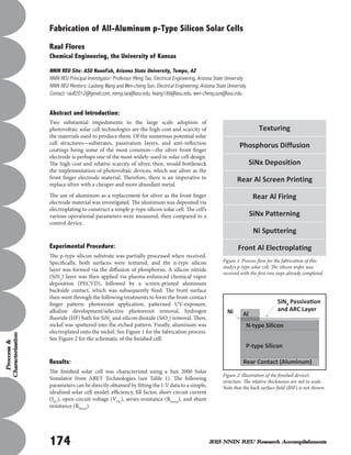
Experimental Procedure:
The p-type silicon substrate was partially processed when received.
Specifically, both surfaces were textured, and the n-type silicon
layer was formed via the diffusion of phosphorus. A silicon nitride
(SiNx
) layer was then applied via plasma-enhanced chemical vapor
deposition (PECVD), followed by a screen-printed aluminum
backside contact, which was subsequently fired. The front surface
then went through the following treatments to form the front-contact
finger pattern: photoresist application, patterned UV-exposure,
alkaline development/selective photoresist removal, hydrogen
fluoride (HF) bath for SiNx
and silicon dioxide (SiO2
) removal. Then,
nickel was sputtered into the etched pattern. Finally, aluminum was
electroplated onto the nickel. See Figure 1 for the fabrication process.
See Figure 2 for the schematic of the finished cell.
Results:
The finished solar cell was characterized using a Sun 2000 Solar
Simulator from ABET Technologies (see Table 1). The following
parameters can be directly obtained by fitting the I-V data to a simple,
idealized solar cell model: efficiency, fill factor, short-circuit current
(JSC
), open-circuit voltage (VOC
), series resistance (RSeries
), and shunt
resistance (RShunt
).
Figure 1: Process flow for the fabrication of this
study’s p-type solar cell. The silicon wafer was
received with the first two steps already completed.
Figure 2: Illustration of the finished device’s
structure. The relative thicknesses are not to scale.
Note that the back surface field (BSF) is not shown.
2. 1752015 NNIN REU Research Accomplishments 1752015 NNIN REU Research Accomplishments
Proccess&
Characterization
Our group’s device was compared to another group’s solar
cell. The reference cell’s structure is almost identical to
this study’s cell; the difference being that the reference cell
uses a silver front contact, and has no intermediary seed
layer between the front contact material and the silicon
substrate, as opposed to the nickel layer in this study’s
device (see Figure 2).
Arguably, the most important parameter in the analysis
of solar cells is efficiency. The efficiency of the reference
cell is significantly higher than our group’s solar cell (a
discrepancy of 4.4 percentage points absolute). The poor
performance of our cell is likely due to a combination
of factors. Fabrication errors in conjunction with non-
optimized cell parameters—parameters being any cell
quantity whose value can be controlled during fabrication,
including: layer thickness, diffusion temperature/time,
front finger dimensions, etc.—are partially culpable for our
device’s poor performance. For instance, it is hypothesized
that the silicon-nickel and/or the aluminum-nickel
interfaces have high contact resistances, which could be
alleviated by optimizing the electroplating procedure.
The fact that our group’s device efficiency was due
to fabrication errors and/or poorly optimized cell
specifications, was corroborated by our cell’s substandard
RShunt
and RSeries
(see Table 1). A poor RShunt
is often
associated with manufacturing defects, which implies that
fabrication errors—such as contamination and sample
damage—occurred during the assembly of the cell. The
potentially high contact resistances between the front
contact layers may contribute to the cell’s high series
resistance. The detrimentally high RSeries
is a probable
contributor to the marginally decreased JSC
and JMP
values
of our cell, relative to the reference (see Table 1).
It should be noted that our group’s solar cell has values for
JSC
and VOC
that are reasonably similar to the reference’s
values. It is therefore believed that if the problems of the
poor RShunt
and RSeries
are addressed, the solar cell designed
by our group will be able to perform at a level comparable
to, or better than, the reference device.
Conclusions and Future Works:
A cell employing an aluminum front contact was fabricated
and characterized. The device has a poor efficiency relative
tothereference,whichislikelyduetosubstandardRSeries
and
RShunt
values. The poor values of RSeries
and RShunt
are due
to fabrication errors and non-optimized cell parameters.
These flaws will have to be addressed to increase the
efficiency of the device, and thus demonstrate the efficacy
of aluminum as an alternative front contact material.
Acknowledgments:
I would like to express my gratitude towards my PI,
Professor Meng Tao, and to my mentors, Laidong Wang
and Wen-cheng Sun, for their guidance and support. I
would also like to thank the National Nanotechnology
Infrastructure Network Research Experience for
Undergraduates (NNIN REU) Program, the National
Science Foundation (NSF), Arizona State University, and
the Center for Solid State Electronics Research for the
support, funding and opportunity provided. This research
was supported by the National Science Foundation under
Grant No. ECCS-0335765.
References:
[1] Tao, C.; Jiang, J.; Tao, M., Natural Resource Limitations to
Terawatt-scale Solar Cells. Solar Energy Materials and Solar Cells
2011, 95 (12), 3176-3180.
[2] Sun, W.C.; Han, X.F.; Tao, M., Electroplating of Al on Silicon in an
Ionic Liquid. Ecs Electrochem Lett 2015, 4 (4), D5-D7.
[3] Sun, W.C.; Zhang, H.; Tracy, C. J.; Tao, M., Electroplated Al as
the Front Electrode in Crystalline-Si Solar Cells. IEEE 42nd
PVSC
Conference.
Table 1: Table of various solar cell parameters (Efficiency, JSC
, VOC
,
RShunt
, and RSeries
) for this study’s device and a reference device.
Also shown: the percent difference between the two solar cell
devices.
![1752015 NNIN REU Research Accomplishments 1752015 NNIN REU Research Accomplishments
Proccess&
Characterization
Our group’s device was compared to another group’s solar
cell. The reference cell’s structure is almost identical to
this study’s cell; the difference being that the reference cell
uses a silver front contact, and has no intermediary seed
layer between the front contact material and the silicon
substrate, as opposed to the nickel layer in this study’s
device (see Figure 2).
Arguably, the most important parameter in the analysis
of solar cells is efficiency. The efficiency of the reference
cell is significantly higher than our group’s solar cell (a
discrepancy of 4.4 percentage points absolute). The poor
performance of our cell is likely due to a combination
of factors. Fabrication errors in conjunction with non-
optimized cell parameters—parameters being any cell
quantity whose value can be controlled during fabrication,
including: layer thickness, diffusion temperature/time,
front finger dimensions, etc.—are partially culpable for our
device’s poor performance. For instance, it is hypothesized
that the silicon-nickel and/or the aluminum-nickel
interfaces have high contact resistances, which could be
alleviated by optimizing the electroplating procedure.
The fact that our group’s device efficiency was due
to fabrication errors and/or poorly optimized cell
specifications, was corroborated by our cell’s substandard
RShunt
and RSeries
(see Table 1). A poor RShunt
is often
associated with manufacturing defects, which implies that
fabrication errors—such as contamination and sample
damage—occurred during the assembly of the cell. The
potentially high contact resistances between the front
contact layers may contribute to the cell’s high series
resistance. The detrimentally high RSeries
is a probable
contributor to the marginally decreased JSC
and JMP
values
of our cell, relative to the reference (see Table 1).
It should be noted that our group’s solar cell has values for
JSC
and VOC
that are reasonably similar to the reference’s
values. It is therefore believed that if the problems of the
poor RShunt
and RSeries
are addressed, the solar cell designed
by our group will be able to perform at a level comparable
to, or better than, the reference device.
Conclusions and Future Works:
A cell employing an aluminum front contact was fabricated
and characterized. The device has a poor efficiency relative
tothereference,whichislikelyduetosubstandardRSeries
and
RShunt
values. The poor values of RSeries
and RShunt
are due
to fabrication errors and non-optimized cell parameters.
These flaws will have to be addressed to increase the
efficiency of the device, and thus demonstrate the efficacy
of aluminum as an alternative front contact material.
Acknowledgments:
I would like to express my gratitude towards my PI,
Professor Meng Tao, and to my mentors, Laidong Wang
and Wen-cheng Sun, for their guidance and support. I
would also like to thank the National Nanotechnology
Infrastructure Network Research Experience for
Undergraduates (NNIN REU) Program, the National
Science Foundation (NSF), Arizona State University, and
the Center for Solid State Electronics Research for the
support, funding and opportunity provided. This research
was supported by the National Science Foundation under
Grant No. ECCS-0335765.
References:
[1] Tao, C.; Jiang, J.; Tao, M., Natural Resource Limitations to
Terawatt-scale Solar Cells. Solar Energy Materials and Solar Cells
2011, 95 (12), 3176-3180.
[2] Sun, W.C.; Han, X.F.; Tao, M., Electroplating of Al on Silicon in an
Ionic Liquid. Ecs Electrochem Lett 2015, 4 (4), D5-D7.
[3] Sun, W.C.; Zhang, H.; Tracy, C. J.; Tao, M., Electroplated Al as
the Front Electrode in Crystalline-Si Solar Cells. IEEE 42nd
PVSC
Conference.
Table 1: Table of various solar cell parameters (Efficiency, JSC
, VOC
,
RShunt
, and RSeries
) for this study’s device and a reference device.
Also shown: the percent difference between the two solar cell
devices.](data:image/gif;base64,R0lGODlhAQABAIAAAAAAAP///yH5BAEAAAAALAAAAAABAAEAAAIBRAA7)