Cfd thermal analysis on laptop cooling system using loop heat pipe technology
Final_Project_ESE_441
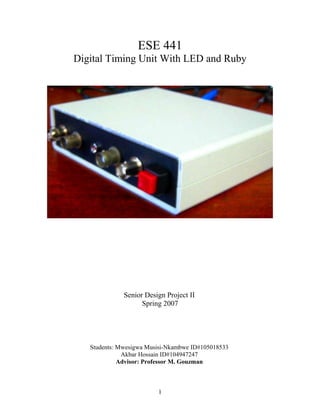
1. ESE 441
Digital Timing Unit With LED and Ruby
Senior Design Project II
Spring 2007
Students: Mwesigwa Musisi-Nkambwe ID#105018533
Akbar Hossain ID#104947247
Advisor: Professor M. Gouzman
1
2. Table of Contents Page
Abstract …………………………………………………………………………………1
1. Goal and Impacts…………………………………………………………………….4
2. Background
Survey……………………………………………………………………………………4
Project Planning………………………………………………………………………….6
3. System Design
Design Constraints ………………………………………………………………………6
Design Considered……………………………………………………………………….7
Final Design……………………………………………………………………………...9
4. System Implementation and Testing
Implementation Problems.………………………………………………………………15
Final Implementation…………………………………………………………………....15
Testing…….…………………………………………………………………………….15
5. Discussion
Mutli-Disciplinary Experience/Issues…………………………………………………...16
Ethical Considerations…………………………………………………………………...16
Impact of Project on Society/Environment……………………………………………...17
Conclusion……………………………………………………………………………...17
Acknowledgements…………………………………………………………………….18
Circuit diagrams and pictures…………...…...…………………………………………19
References…………………………………………….………………………………..25
2
3. Abstract
In this senior design project, a digital timing unit will be built to ensure
functioning of a temperature sensor based on fluorescence lifetime of ruby crystal. This
subsystem should provide 10us and 50us pulses for LED which will be added in the final
stage of the project. A survey of work done by previous investigators will be key role to
start planning the project. Modification will then be done to the timing unit using Eagle
software. The work of engineers is the link between perceived social needs and
commercial applications. Therefore, this timing unit will be primarily cost effective and
should be easy to function. The operation of the timing unit will also be discussed in
detail to ensure that the audience can fully comprehend and appreciate the use of this
timing control unit.
3
4. Goals and Impacts:
The goal of this project is to build a device that is innovative, unique, and robust
and an efficient temperature sensor. The first phase will be to build the timing unit which
will enable the functioning of temperature sensor based on fluorescence lifetime of ruby
that will be assembled in the next phase of the project. The timing unit uses only standard
components and hence has low cost to manufacture. Temperature sensors using
fluorescent lifetime of ruby crystal have lot of advantages of wide dynamic range,
intrinsic immunity to electromagnetic interference, small size, high sensitivity, high
accuracy, fast response and calibration is unnecessary anymore. Most current sensors are
affected by electromagnetic fields but this new sensor will be prone to such affects. This
temperature sensor can be used to measure temperatures of houses, hospitals, machinery
of which a prime application would be in automotive engines. Millions of people’s lives
are at stake if malfunction occurs in temperature sensors on mass transportation such as
airplanes, trains, buses, etc. One of the key causes for the tragic accident of the Columbia
space shuttle was the failure of the temperature sensor. Therefore, these revolutionary
temperature sensors are expected for use in the temperature measurements of
extraordinary conditions such as in plasma, high frequency induction heating, and high
temperature [1]. Hence the need for such this sensor is immense and will be very
beneficial to people in all disciplines.
Background
Survey
Similar work on fluorescence based temperature sensor was done on
Quasidistributed fluorescence-based optical fiber temperature sensor system by T. Sun,
Z. Y. Zhang, K. T. V. Grattan, and A. W. Palmer: Department of Electrical, Electronic
and Information Engineering, City University, London, United Kingdom [2]. In their
work, a quasidistributed multipoint intrinsic decay time-based fiber optic fluorescent
sensor system was reported. Their research was aimed at finding a simple, yet accurate,
system using several doped fiber elements linked on a single intrinsic fiber network. An
analysis scheme using Prony’s method has been reported which enables exponential
decays from either single-material or two material and quasidistributed sensors to be
deconvolved and thus data and associated measure and information encoded in each
individual signal to be recovered. In this work, in the development of quasidistributed
temperature sensor algorithms based on Prony’s method are used for the estimation of
exponential time constants of convolved triple exponential fluorescence decay, each
corresponding to a different-point temperature. An infrared laser operating at a center
4
5. wavelength of 813 nm was used as the excitation light source and its output was
modulated by a pulse signal generated by the digital output port of a desktop computer.
Our temperature sensor will contain a single fluorescence element, ruby crystal and will
use a LED of which the pulse width will be controlled by the preliminary design of the
timing control unit, hence making it cheaper.
A similar digital timing unit as ours was also built by Philip Sgroi and Chris Lo
who were students of Stony Brook University, but their sub-system was used to design a
sensing system for photon counting.
Measurement of window glass temperature with a Fluorescence Intensity Ratio
(FIR) approach was done by Maria Cristina Vergara, Victoria University [3]. A prototype
temperature sensor using the FIR technique was designed to measure the surface
temperature of window glass during a fire, whereas our temperature sensor will employ
the use of fluorescent lifetime (FL) scheme. Comparisons of the two schemes show that
at very low temperatures, the FIR method exhibits a significant variation with
temperature, while the response of the FL method becomes constant with its sensitivity
approaching zero [1].
Fig 1. The lifetime ratio data as a function of the scaled Fig 2. Normalized FIR data as a function
temperature for crystals of ruby, alexandrite, Cr31:YAG of the scaled temperature for Er31-doped fiber,
and bulk Pr31:ZBLAN. Yb31-doped fiber and bulk Pr31:ZBLAN.
5
6. Project Planning
Knowledge of digital systems (ESE 218) was crucial. The principle of the
workings of NAND gates was essential in the design because in some case they were
used as inverters. Three 74LS00N chips were used to implement the NAND gates into
the unit's circuitry. Knowledge in analog circuitry is important in order to troubleshoot
the PCB so that the design requirements are met. Thus knowledge of ESE 211, 314 and
324 was beneficial as the oscilloscope was rigorously used to see the timing pulses and
tuning had to be done to optimize the view. It was through these laboratory works that
testing, measuring and troubleshooting of the timing unit proved to be very fascinating
and fruitful. Additional knowledge of the 555 timers’ configurations was investigated,
datasheets from the Fairchild website
(http://www.fairchildsemi.com/technical_information/datasheets.html) were used and
tutorials on 555 timers were read (www.uoguelph.ca/~antoon/gadgets/555/555.html). The
program Eagle was used to design the PCB board. Online tutorials provided the
knowledge of designing PCB boards. The board was printed with Eagle and etched in the
laboratory. Prof. Guzman provided the expertise needed to etch and drill holes in the
board prior to soldering circuit elements on the board.
System Design
Design Constraints
Engineers apply established principles drawn from mathematics and science in
order to develop economical solutions to technical problems [4]. The work of engineers is
the link between perceived social needs and commercial applications. Therefore, this
timing unit had to be primarily cost effective and that was achieved by employing
conventional timers, NAND gates, resistors and capacitors.
Component Unit Price ($)
LM555CM 0.10720
SN74LS00N 0.56000
Table 1: Unit price for the LM555 timer and SN74LS00N Quad-2-input NAND gate [5]
Since these items would be purchased in bulk for manufacturing purposes, the prices of
these components would decrease. In addition, other costs incurred are also quite
negligible since they were all standard elements. Another consideration taken into
account was the ease of the functioning of the timing unit. The pulse widths of the timers
can be changed by adjusting the respective timer’s potentiometers.
6
7. Design Considered
There were modifications done and a comparison of the before and after pictorial
view can be seen in Fig 3. The copper wires were thickened in order to minimize leakage
and therefore improve performance of the PCB as a whole.
Figure 3a: Original design of PCB board
Figure 3b: Modified design of PCB board
7
8. A box for the timing unit cannot be left bare. A casing has to be made so that switches,
LED (from here on we will refer as LED1) to indicate on or off state and BNC
connectors for the appropriate powering can be added.
All 5 BNC connectors were at first placed in consecutive order and the LED1 and the
switch. The next modification in the design was to place the BNC connectors closer to
the input ports and then accordingly label them. This was an efficient designing scheme
to limit the use of long wires and therefore limit parasitic currents in the timing unit. The
LED (from here forth, we will refer to LED 2) emitting green light and the photo sensor
are not found on the board or inside the case in which they were put. Instead they are
external to the timing unit that was designed and built in the first stage of the project.
BNC connectors mounted on the outside of the box that the unit was placed in where
used to connect the LED and photo sensor to the unit.
A holder was designed to hold the LED and fiber optic cable that would be connected to
the timing unit. Below are the screenshots of the actual design files for the holder.
8
9. Final Design
The digital control unit uses five LM555 timers and three 74LS00 quad 2-input
NAND gates ICs to collect data from an external input, a simple time-gating technique is
used. This is done by creating two timing windows each having respective lengths t1 and
t2. In this specific application t1 = 10μs and t2 = 50μs.
The first timer, shown in Figure 4, was configured in the astable timer mode; this
made it a frequency generator. A pulse frequency of 100Hz was set by selecting specific
capacitors and resistances. The astable mode was achieved by shorting the trigger pin to
the threshold pin on the LM555 timer chip. The remaining timers were set in monostable
mode, this was achieved by applying 1/3 Vcc to the trigger pin. Figure 7 gives a block
diagram with the accompanying pins of the LM555 timer. The specific pulse widths were
calculated with the time constant τ = RC. The potentiometer resistor adds some flexibility
to the each timer’s time constant by adjust R in the time constant equation.
Timer 2 is used to send out pulses to a device, in this specific application this will
be an LED. Timer 3 generates a delay that is needed in this application to make sure the
LED is turned off before timers 4 and 5 use timing windows t1 and t2 to collect data, in
this application in the time intervals t1 and t2 photons will be counted. The pulses from
timers 1 thru 5 are shown below.
9
11. Fig 5. Initial pulse from timer 1 that was used as a frequency generator
The NAND gates found in the 74LS00N are used to shorten pulses from the LM555
timers before being fed into their consecutive timers. The pulses generated by the outputs
of these timers are too long to trigger a timer so by sending the pulses through two
NAND gates and a capacitor we are able to get a pulse that is short enough to drive the
timer. In Fig 5 this is illustrated, the incoming signal (signal 1) is fed into pins 1, 2 and 4
of the 74LS00N as shown. This signal is then feed to pins 1 and 2 giving us signal 2
(inverted signal 1). Signal 2 is then used to charge a capacitor though a resistor to
produce signal 3. The capacitor charges up then discharges delaying the signal’s fall time.
Signal 3 it can then NAND with the original signal 1 at pin 5 to produce signal 4 at pin 6.
This is then feed to the next LM555 timer. This configuration is repeated as shown in the
circuit diagram on page 15.
LED1 was placed in between the two BNCs to indicate when the 5V power is being
supplied. This is vital to the user in knowing that the timing unit is turned on. The board
was fixed in place by being drilled into the box. Spacers were used and adjusted to leave
optimum room from the board to the case. The signal from timer 5 is NAND so is the
signal from timer 4. After being NAND with the input these signals are sent to the
outputs Out1 and Out2. The LED2 was connected to P2 thru a BNC connector. The
photo-sensor that was used to visualize the pulses was put into a cylinder enclosed in
dark black paper to block out any external light that will disrupt readings from the photo-
sensor.
11
13. Fig 7. Timing unit with internal block diagram of 74SL00n and LM555
13
14. A BNC connector was used to connect the timing unit to an LED that was placed in a
holder made of PCB material, below is a picture of the proposed
The X denotes the place where the photo sensor will be placed. In this senior design
project this part was not reached. The holders were held together by screws and spacers.
14
15. System Implementation and Testing
Implementation Problems
The power connection that connects the unit to power was loose so sometimes the unit
would turn off. This was resolved by putting in a connector with larger diameter. The
signal that was used to power the LED2 had the right pulse lengths that we needed but
the signal was inverted so the BNC connector that connects the LED to P2 was modified
so instead of its outer rim connecting to ground like all the other BNC connectors on the
board it was connected to the negative terminal of P2, this gave us the signal we desired
at the BNC connector.
Final Implementation
The original unit that was designed in the first stage was put into a box with an on/off
button. A red LED was put on the front of the casing to indicate when the unit was on or
off. BNC connectors were put on the front of box to enable connections to external
devices (in our case a LED and a case with a ruby was to be connected here). The back of
the box had power input, where a 120VAC/5V DC converter was connected, making it
easy for the unit to be connected to a wall power outlet instead of the in lab power supply
that was used in the first part of the project.
All pulses from all timers were rechecked to make sure they still output the pulses they
had previously output. A LED and fiber optic cable were put in a holder that kept them
stationary so when illuminated by the 10us pulse from the timing unit the loss of light
travelling in a straight line was less. The fiber optic cable coming out of the holder was
then connected to a black container that held the ruby.
Testing
The l signal that was sent to the LED2 was checked with an oscilloscope, but this was not
what the photo sensor read. Even when the LED2 was placed in. This was fixed by
testing the pulses in that came from the photo-sensor in a dark environment. The
oscilloscope has to be triggered many times and the noise that was present while
checking for the pulse windows at the collector of the BJT, noise rejection mode was
made use of. The BJT was taken out and placed into a breadboard as we needed to
frequently check for pulses. This testing could not have been done if the transistor was
soldered into the printed circuit board. After looking at the circuit for a second time and
making slight alterations the desired 10us pulse needed to illuminate the LED was
observed
15
16. Results and Discussion
The circuit board that was built worked the way that was expected. Signals from timers
and NAND gates were as expected the desired signal needed to power the LED that
would illuminate the ruby was achieved. The desired signal from the 2N2222 BJT
collector as shown below was achieved the signal that was check at the output
coressponded with it. All signals were checked with an oscilloscope. The circuitry on the
board was check and no faults were found.
Mutli-Disciplinary Experience/Issues
The team consisted of two members who were majoring in Electrical
Engineering. Akbar Hossain used his knowledge with Eagle to improve the PCB design
that was used in previous applications of the board. Mwesigwa Musisi-Nkambwe used
his analog circuitry knowledge to assemble the board. A weekly schedule was setup in a
way that each of the engineers would come into the laboratory thrice. Once working
together and the other times they would come independently due to class timing conflicts.
This made a flow of progress as each engineer would do independent work on the timing
board rather than relying on just one to troubleshoot and assemble the board. Since both
engineers took the same coursework, confusions could be cleared out by small
discussions rather than having one student specializing on hardware and another on
software. Then, the situation would call for gaps in comprehension of the design
requirements and hence delay coordination and progress. This project was entirely based
in hardware and thus was very interesting for both of us having vast hardware
knowledge. The report was also divided into parts and we had both coordinated together
to make sure both were on track and thus resulted in having an affinity to research more
and clear all doubts about operations of the timing unit.
Ethical considerations
The essence of going to school would be to create ideas by one rather than
depending on others. As this would promote learning and ensure interest in the disciple
one would want to build a future in. That all can be compromised if one is not true and
relies on others. This would not make one achieve dreams and it is through these believes
that we have worked to get the time pulses from our own board rather than using the
previous board to get the results to make this report. As stated earlier, a similar digital
16
17. control unit was made by ESE 440 students. Since we were ethical in the terms outlines
above, we can provide real-time pulses using our board upon request by Professor
Gouzman. Regardless to say but that made us learn functioning of the board and
hopefully will make us excel in finishing the fluorescence lifetime-based sensor within
the next three months.
Impact of Project on Society/Environment
Refer to Goals and Impacts.
Conclusion
The digital timing unit built in the first part of the project provided the necessary
circuitry needed to build the temperature sensor in the second and final part of the
project. Two counting windows were measured, one being 10μs and the other being 50μs.
These were part of the design requirements and therefore we were successful in
completing a functioning timing unit. One timer was burned while testing the board and a
there were a couple of leads that were not soldered and were not visible to the naked eye.
These cumbersome issues had to be resolved following the signals from and to the timers.
The design of the previous board was modified and various constraints were met and
ethical principles were followed in the design of this timing unit.
In the second part of the project the timing unit was recalibrated to make sure that
we still met our timing constraints, the unit was put in a box that had inputs for power,
inputs and outputs. The output of the unit was tested and with an oscilloscope, the
2N2222 BJT that was to used to amplify the signal from the second timer was not
working properly so it was replaced. The actually signal from the BJT’s collector
terminal which was used to power the LED was as expected, but the signal at the BNC
connector where the LED had a lot of additional noised added to it. All connections on
the board were intact and the signal from the BJT’s collector terminal that was directly
connected to the BNC connector was what was expected. After a complete review of the
whole circuit and close monitoring of the output at the BNC connecter the desired output
was achieved. A LED and fiber optic cable in a holder that had a BNC connector
(making it’s connectivity to the timing unit less cumbersome) was connected to the
timing unit. On the other end of the holder was a container that held the ruby. The project
up to this point was a success the photo sensor will be the next stage in the ongoing
project.
17
18. Acknowledgements
We would like to thank Professor Gouzman for his advice, help and
supervision in our project. We learned various techniques in analyzing analog circuitry
and therefore are very grateful for getting such a wonderful opportunity.
18
21. Figure 10. Top back view of PCB
Figure 11.Top left view
21
22. Figure 12. Top right view
Figure 13 – Circuit board in case with BNC connectors and power input.
22
23. Figure 14. Top view of LED holder with wires from BNC connector on the right and
fiber optic cable coming out on the right.
Figure 15. back of LED holder
23
24. Figure 16. Front of LED Holder
Figure 17. Timining unit connected to holder with led and fiber optic output.
24