
Recommended
Recommended
More Related Content
What's hot
What's hot (20)
Similar to INTELLIGENT POWER MODULE Model No : PEC16DSMO1
Similar to INTELLIGENT POWER MODULE Model No : PEC16DSMO1 (20)
Recently uploaded
Recently uploaded (20)
INTELLIGENT POWER MODULE Model No : PEC16DSMO1
- 1. INTELLIGENT POWER MODULE (Model No : PEC16DSMO1) User Manual Version 2.0 Technical Clarification /Suggestion : N / F Technical Support Division, Vi Microsystems Pvt. Ltd., Plot No :75,Electronics Estate, Perungudi,Chennai - 600 096,INDIA. Ph: 91- 44-4204 8142, 91-44-2496 3142 Mail : service@vimicrosystems.com, Web : www.vimicrosystems.com
- 2. CONTENTS 1. Intelligent Power Module 1.1 Introduction 1 1.2 About Our Trainer Front panel view 2 Front panel Description 3 Connector Details 4 1.3 Specifications 5 1.4 Applications 9 2. Hardware Description 10 2.1 Intelligent Power Module 11 2.2 IPM Protection 11 i. Self protection 11 ii. Under- voltage lock-out protection 12 iii. Over - temperature protection 13 iv. Over - current protection 14 v. Short circuit protection 15 2.3 Interface Circuit for Seven - pack IPM 16 2.4 Handling Precaution for IPM 17 2.5 High Voltage Input DC - DC Converter 18 2.6 IPM Power Supply 19 3. Voltage and Current Sensor 20 3.1 Hall effect 21 3.2 Hall effect current transducer 22 3.3 Hall Effect Closed Loop Current Transducers 22 3.4 Unipolar Power Supply 26 3.5 Hall Effect Closed Loop Voltage Transducers 27 4. Signal Conditioner 28 5. Protection Circuit 31 6. Opto Coupler 32
- 3. 7. Three Phase Diode Bridge Rectifier 33 8. Speed Sensor 8.1 Optical Encoder 34 8.2 Quadrature Encoder Pulse i. Introduction 35 ii. QEP Inputs 36 iii. Two Channel Optical Encoder 37 8.3 Connector Details 39 9. Frequency to Voltage Converter 40 10. General Instruction 41
- 4. PREFACE PEC16DSM01 is a reference manual for INTELLIGENT POWER MODULE. This manual briefly explains each and every section present in the module. We hope that these modules will help in setting up a good power electronics laboratory in a simple manner. It is laboratory type module, so power electronics staff can teach the students easily with guidance of technical reference manual and our installation engineer. Power electronics modules are installed by our Qualified engineer, hence customer can clarify the technical details, service tips thoroughly from our installation engineer about module. This is very helpful to solve the occurrence of minor fault (cause due to mishandling / poor maintenance) without our service engineer. Earnest effort has been made to present details in a simple fashion. We do welcome suggestions regarding the improvement of module and this manual. Write to Technical Support Division, Vi Microsystems Pvt. Ltd., Plot No. 75, Electronics Estate, Perungudi, Chennai-600 096. India Phone: 91-44-2496 1842, 2496 1852. E-mail: sales@vimicrosystems.com
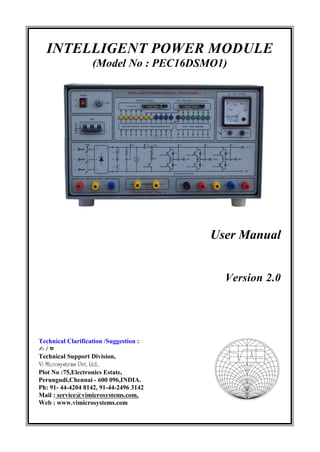
- 5. IPM BASED POWER MODULE PEC16DSMO1 Vi Microsystems Pvt. Ltd., [ 1 ] 1. INTELLIGENT POWER MODULE 1.1 INTRODUCTION IPM basedpowermoduleworkasDC- DC Converter (Chopper)or DC-AC Converter (Inverter). It works using a IGBT based IPM and works on basis of software from DSP Processor. The power module can be used for studying the operation of chopper, three phase inverter, single phase inverter and speed control of three phase induction motor, single phase induction motor. Intelligent Power Modules (IPMs) are advanced hybrid power devices that combine high speed, low loss IGBTs with optimized gate drive and protection circuitry. Highly effective over-current and short-circuit protection is realized through the use of advanced current sense IGBT chips that allow continuous monitoring of power device current. System reliability is further enhanced by the IPM's integrated over temperature and under voltage lock out protection. IPM has been optimized for minimum switching losses in order to meet industry demands for acoustically noiseless inverters with carrier frequencies up to 20KHz. The built in gate drive and protection has been carefully designed to minimize the components required for the user supplied interface circuit. This manual provides details of the hardware description of IPM based power module, it also provides the step-by step procedure of the various experiments. 1.2 ABOUT OUR TRAINER The following figure shows the front panel of "IPM BASED POWER MODULE PEC16DSMOl". Figure - 1
- 6. IPM BASED POWER MODULE PEC16DSMO1 Vi Microsystems Pvt. Ltd., [ 2 ] FRONT PANEL VIEW Figure - 1.1
- 7. IPM BASED POWER MODULE PEC16DSMO1 Vi Microsystems Pvt. Ltd., [ 3 ] FRONT PANEL DESCRIPTION R,Y,B = Applied to 3 phase AC input supply. U,V,W = Three phase R, Y, B output terminals. BR1 & BR2 = Breaking Rheostat (470S - 2A). +HV = Rectifier with filter DC output voltage (DC link voltage). Voltmeter = Read the DC link voltage. V/2 = Voltage across V/2 is half of the DC link voltage. Feed back signals (Isolated current/voltage/speed sensor output) 1 2 3 1 2I , I , I = 3 phase R,Y,B current transducer output currents are I , I , 3I respectively and measure this current across the terminals U, V and W. DCV = DC link voltage (voltage transducer output). DCI = DC link current ( current transducer output). N(Speed) = Analog voltage ( 0 - 5V). F = Fault output signal comes from IPM, when over temperature/current occurs. MCB = Power ON/OFF the 3 phase AC supply. Power = Power ON/OFF the control circuits. IGBT - PWM Inputs (from controller) PWM1,.... PWM6 = PWM pulses are coming from controller. PWM output High - 5V = IGBT ON. Low - 0V = IGBT OFF. CAP1,.......CAP6 = Capture input to processor. Protection Circuit RST = Reset the protection circuit, then 'SD' LED will be off. SD = Shut down LED will glow, when over voltage/current occurs in power circuit.
- 8. IPM BASED POWER MODULE PEC16DSMO1 Vi Microsystems Pvt. Ltd., [ 4 ] CONNECTOR DETAILS Fig - 1.2 Pin Details ( The following specific pin numbers are used to your own design applications. Don’t change the specific pin numbers). 34 pin FRC Connector 26 Pin FRC Connector 1 PWM1 5 N - SPEED 3 PWM2 7 I1(IR) 5 PWM3 9 I2 (IY) 7 PWM4 11 AFOUT 9 PWM5 21 IDC 11 PWM6 23 I3 (IB) 2,4,13,15,17,19 No Connection 25 VDC 21 BREAK 1,2,3,4,13,15,1 7,19 No Connection 23 SD 25 CAP1/QEP1/IOPC4 12,14,16,18,20, 22,24,26 GND 27 CAP2/QEP2/IOPC5 29 CAP3/IOPC6 Note : Pin No 5 - N (Speed) Analog voltage (0-5V) is apply to directly. Don’t apply to speed pulse signal. 31 CAP4/IOPC7 33 PDPINT 6,8,10,12,14,16,18,20, 22,24,26,28,30,32,34 GND Pin No - 25, 27, 29, 31 (Speed feed back pulse signal - is directly apply to required pin numbers 1 3 5 7 9 11 13 15 17 2 6 12 16 20 24 28 32 34302622181484 10 292725232119 31 33 34 Pin FRC 26 Pin FRC 19 21 23 251715131197531 104 8 14 18 22 262420161262
- 9. IPM BASED POWER MODULE PEC16DSMO1 Vi Microsystems Pvt. Ltd., [ 5 ] 1.3 SPECIFICATIONS Input * Three - phase AC supply (415V±10%) * Single - phase AC supply (230V±10%) Output * DC Link voltage - 750V DC. * Max. Current - 8A. * Three- phase variable voltage & variable frequency. * Fixed and variable DC voltage * Single - phase variable voltage & variable frequency. Test point Voltage ratings 1. IDC Fig - 1.3 2. I1, I2, I3 No Load ( Normal) (V) = 1.6V Apply Load 1A (V) = 1.6 + 0.17 SinTt Apply Load 2A (V) = 1.6 + 0.34 SinTt Apply Load 3A (V) = 1.6 + 0.51 SinTt Apply Load 4A (V) = 1.6 + 0.68 SinTt t V Apply Load t ( No Load ) 0 Upto 1A Normal .33V
- 10. IPM BASED POWER MODULE PEC16DSMO1 Vi Microsystems Pvt. Ltd., [ 6 ] Fig - 1.4 0 t .17V .34V .51V .68V 0 0 0 t t t t t t 1.6V Load = 4A Load = 3A Load = 2A No Load Load = 1A 1.6V 1.6V 1.6V 1.6V 0 V t t
- 11. IPM BASED POWER MODULE PEC16DSMO1 Vi Microsystems Pvt. Ltd., [ 7 ] The figure -1.4 the output frequency is depends upon PWM techniques. i. Sinusoidal PWM ii. Space vector PWM TYPE OF PWM FREQUENCY RANGE Minimum Maximum Sinusoidal 1 Hz 50Hz Space Vector 1 Hz 50Hz Note: IGBT Switching Frequency - 5KHz to 10KHz. Dead time - 5:s(Minimum). VDC - Maximum value of DC link voltage = 750V at that time output voltage of test point terminal VDC = 3.3V. Fault - Fault occurred in a system. The Maximum output voltage of fault terminal = 3.3V. Speed - Max voltage of speed terminal is 2.6V at Motor rated speed 1500rpm. Break - Break pulse output Amplitude = 5V. PWM1 to PWM6- The Max Amplitude of PW1 to PWM6 (test points) = 5V with respect to GND.
- 12. IPM BASED POWER MODULE PEC16DSMO1 Vi Microsystems Pvt. Ltd., [ 8 ] DEVICE SPECIFICATIONS Bridge Rectifier - 3N diode bridge Rectifier (60A,1200V) IGBT Intelligent power module ( 25A, 1200V) * Switching frequency = 20KHz (Max), 10KHz Nominal. * Braking of IGBT = 10A, 1200V (Max). 6A Nominal. FO* Fault output current (I ) = 20mA (Max) FO* Fault output voltage (V ) = 20V (Max) Voltage Transducer (LV25-P) PN* Primary nominal r.m.s. current (I ) = 10mA PN* Primary nominal r.m.s voltage (V ) = 10 to 500V SN* Secondary nominal r.m.s current (I ) = 25mA Current Transducer (LTS 25-NP) PN* Primary nominal r.m.s current (I ) = 8-12-25A b* R.M.S rated voltage( V ) = 525V out p* Analog output voltage (V ) = 2.5V (I = 0) IPM Power Supply * Output = Four +15V supply Max power=3W Rms* Primary to Secondary isolation = 2500 V , one minute Rms,* Secondary to Secondary isolation voltage = 1500 V one minute High Voltage Input DC-DC Converter * input voltage (Vin) = 113V to 400V DC * output voltage (Vout) = 18 to 22 V DC * Load Current = 220mA For more details of device specifications refer the data sheets.
- 13. IPM BASED POWER MODULE PEC16DSMO1 Vi Microsystems Pvt. Ltd., [ 9 ] 1.4 APPLICATIONS The IPM Based power module can be used for the following study experiments. i. To study the output voltage/current wave forms of 1. Three phase inverter with star connected R and RL Load . 2. Three phase inverter with delta connected R and RL Load 3. Four Quadrant chopper unipolar switching with R and RL-Load. 4. Single Quadrant chopper with R and RL-Load. ii. To study the motor speed control (Open Loop) 5. Separately excited DC shunt motor by using four quadrant chopper with unipolar 6. Three phase induction motor by using different PWM techniques (sinusoidal, V/F and space vector Modulation). 7. Single phase induction motor by using sinusoidal pulse width modulation technique only. iii. To study the motor speed control (Closed Loop) 8. Separately excited DC shunt motor by using four quadrant chopper with unipolar 9. Three phase induction motor by using different PWM techniques (sinusoidal, V/F and space vector Modulation). 10. Single phase induction motor by using sinusoidal pulse width modulation technique only. Note The following motor controls are possible in PEC16DSMO1 module * Brush less DC motor (BLDC) * Permanent Magnet Synchronous Motor (PMSM)
- 14. IPM BASED POWER MODULE PEC16DSMO1 Vi Microsystems Pvt. Ltd., [ 10 ] 2. HARDWARE DESCRIPTION Figure - 2 Block Diagram for IPM based power module The block diagram of IPM Based Power Module (PEC16DSMOl) is shown in Figure (2). It consists of a 1. Intelligent Power Module 2. Voltage and Current Sensor 3. Signal Conditioner 4. Protection Circuit 5. Opto Coupler 6. 3 N diode bridge Rectifier 7. Speed Sensor 8. Frequency to Voltage converter +15V +15V +15V 0V + - ISOLATED POWER SUPPLY HIGH VOLTAGE INPUT DC-DC CONVERTER DSP / MICRO - CONTROLLER U V W VDC VOLTAGE & CURRENT CONDITIONAR SIGNAL BRIDGE RECTIFIER 3-Ø DIODE IPM - PM25RSB120 SENSOR PROTECTION CIRCUIT SPEED SENSOR VDC IDC BYR SUPPLY 3 Ø AC MCB P N B INPUT SIGNAL FAULT OUTPUT I1 2I 3I 4I 3 Ø MOTOR HGND v+ OPTO COUPLER (3) OPTO COUPLER (1) OPTO COUPLER (2) PC AFOUT IR IY IB PDPINT PWM BREAK CONVERTER F/V IPM BASED POWER MODULE [ PEC16DSMO1 ]
- 15. IPM BASED POWER MODULE PEC16DSMO1 Vi Microsystems Pvt. Ltd., [ 11 ] 2.1 INTELLIGENT POWER MODULE Mitsubishi Intelligent power Modules utilize many of the same field proven module packaging technologies used in Mitsubishi IGBT modules. Cost effective implementation of the built in gate drive and protection circuits over a wide range of current ratings was achieved using two different packaging techniques. Low power devices use a multilayer epoxy isolation system while medium and high power devices use ceramic isolation. 2.2 IPM PROTECTION The following protection schemes available for Intelligent power Module. i. Self Protection ii. Under-Voltage Lock-Out Protection iii. Over-Temperature Protection iv. Over-Current Protection v. Short Circuit Protection i. SELF PROTECTION IPM (Intelligent power Modules) have sophisticated built-in protection circuits that prevent the power devices from being damaged should the system multifunction or be over stressed IPM internally builded the fault detection and shut down schemes that allow maximum utilization of power device capability without compromising reliability Control supply under -voltage, over- temperature, over-current, and short-circuit protection are all provided by the IPM's internal gate control circuits. A fault output signal is provided to alert the system controller if any of the protection circuits are activated. Figure 2.1.1 is a block diagram showing the IPMs internally integrated functions. This diagram also shows the isolated interface circuits and control power supply that must be provided by the user. The internal gate control circuit requires only a simple +15V DC supply. Specially designed gate drive circuits eliminate the need for a negative supply to off bias the IGBT. The IPM control input is designed to interface with Optocoupled transistors with a minimum of external components. Figure - 2.1.1 IPM Functional Diagram
- 16. IPM BASED POWER MODULE PEC16DSMO1 Vi Microsystems Pvt. Ltd., [ 12 ] ii. UNDER-VOLTAGE LOCK-OUT PROTECTION Figure - 2.1.2 Operation Of Under - Voltage Lockout TheIntelligent PowerModule's internal control circuits operate from anisolated15VDC supply. If for any reason, the voltage of this supply drops below the specified under-voltage trip level t(Uv , the power devices will be turned off and a fault signal will be generated. small glitches less duvthan the specified t in length will not affect the operation of the control circuitry and will be ignored by the under voltage protection circuit .In order for normal operation to resume, the supply voltage must exceed the under-voltage reset level (Uvr). Operation of the under voltage protection circuit will also occur during power up and power down of the control supply. This operation is normal and the system controller's program should fotake the fault output delay (t ) into account. Figure - 2.1.2 is a timing diagram showing the operation of the under-voltage lock-out protection circuit. In this diagram an active low input signal is applied to the input pin of the IPM by the system controller. The effects of control supply power up, power down and failure on the power device gate drive and fault output are shown. Caution 1. Application of the main bus voltage at a rate greater than 20V/µs before the control power supply is on and stabilized may cause destruction of the power devices. 2. Voltage ripple on the control power supply with dv/dt in excess of 5V/µs may cause a false trip of the UV lock-out.
- 17. IPM BASED POWER MODULE PEC16DSMO1 Vi Microsystems Pvt. Ltd., [ 13 ] iii. OVER-TEMPERATURE PROTECTION The Intelligent power Module has a temperature sensor mounted on the isolating base plate near the IGBT chips. If the temperature of the base plate exceeds the over temperature trip level (OT) the IPMs internal control circuit will protect the power devices by disabling the gate drive and ignoring the control input signal until the over temperature condition has subsided. In six and seven pack modules all three low side devices will be turned off and a low side fault signal will be generated. High side switches are unaffected and can still be turned on and off by the system controller. Similarly, in dual type modules only low side device is disabled. The fault output will remain as long as the over temperature condition exists. When the temperature falls below the over temperature reset level (OTr ), and the control input is high (off state) the power device will be enabled and normal operation will resume at the next low(on) input signal. Figure2.1.3 is a timing diagram showing the operation of the over temperature protection circuit. The over temperature function provides effective protection against overloads and cooling system failures in most applications. However, it does not guarantee that the maximum junction temperature rating of the IGBT chip will never be exceeded. In cases of abnormally high losses such as failure of the system controller to properly regulate current or excessively high switching frequency it is possible for IGBT chip to exceed Tf(max) before the base plate reaches the OT trip level. Figure - 2.1.3 Operation of Over - Temperature Caution Tripping of the over-Temperature protection is an indication of stressful operation. Repetitive tripping should be avoided.
- 18. IPM BASED POWER MODULE PEC16DSMO1 Vi Microsystems Pvt. Ltd., [ 14 ] iv. OVER-CURRENT PROTECTION The IPM uses current sensing IGBT chips to continuously monitor power device current. If the current though the intelligent power Module exceeds the specified over current trip level (OC) for a period longer than toff (OC). The IPMs internal control circuit will protect the power device by disabling the gate drive and generating a fault output signal. The timing of the over- current protection is shown in Figure2.1.4. The toff (OC) delay is implemented in order to avoid tripping of the OC protection on short pulses of current above the OC level that are not dangerous for the power device. When an over-current is detected a controlled shut down is initialized and a fault output is generated. The controlled shut down lowers the turn-off di/dt which helps to control transient voltages that can occur during shut down from high fault currents. Most intelligent modules use the two step shutdown depicted in Figure 2.1.4 the two step shutdown, the gate voltage is reduced to an intermediate voltage causing the current through the device to drop slowly to a low level. Then, about 5µs later , the gate voltage is reduced to zero completing the shut down. Some of the large six and seven pack IPMs use an active ramp of gate voltage to achieve the desired reduction in turn off di/dt under high fault currents. Figure - 2.1.4 Operation of Over-Current and Short-Circuit protection
- 19. IPM BASED POWER MODULE PEC16DSMO1 Vi Microsystems Pvt. Ltd., [ 15 ] V. SHORT CIRCUIT PROTECTION If a load short circuit occurs or the system controller malfunctions causing a shoot through, the IPMs built in short circuit protection will prevent the IGBTs from being damaged. When the current, through the IGBT exceeds the short circuit trip level (SC), an immediate controlled shutdown is initiated and a fault output is generated. The same controlled shutdown, techniques used in the over current protection are used in the over current protection are used to help control transient voltages during short circuit shut down. The short circuit protection provided by the IPM uses actual current measurement to detect dangerous conditions. This type of protection is faster and more reliable than conventional out- of-saturation protection schemes. Figure 2.1.4 is a timing diagram showing the operation of the short circuit protection. To reduce the response time between SC detection and SC shutdown, a real time current control circuit (RTC) has been adopted. The RTC bypasses all but the final stage of the IGBT driver in SC operation thereby reducing the response time to less than 100 ns. Caution 1. Tripping of the over current and short circuit protection indicates stressful operation of the IGBT. Repetitive tripping must be avoided. 2. Highsurge voltages can occur during emergency shutdown.Lowinductancebusworkand snubbers are recommended.
- 20. IPM BASED POWER MODULE PEC16DSMO1 Vi Microsystems Pvt. Ltd., [ 16 ] 2.3 INTERFACE CIRCUIT FOR SEVEN-PACK IPM The following Figure 2.1.5 show the interface circuit for seven-pack IPM Figure - 2.1.5 Interface Circuit for Seven - Pack IPM
- 21. IPM BASED POWER MODULE PEC16DSMO1 Vi Microsystems Pvt. Ltd., [ 17 ] 2.4. HANDLING PRECAUTIONS FOR IPM i. Electrical Considerations * Apply proper control voltages and input signals before static testing. * Carefully check wiring of control voltage sources and input signals. Miswiring may destroy the integrated gate control circuit. * When measuring leakage current always ramp the curve tracer voltage up from zero. Ramp voltage back down before disconnecting the device. Never apply a voltage greater than the VCES rating of the device. * When measuring saturation voltage low inductance text fixtures must be used. Inductive surge voltages can exceed device ratings. ii. Mechanical Considerations * Avoid mechanical shock. The module uses ceramic isolation that can be cracked if the module is dropped. * Do not bend the power terminals. Litting or twisting the power terminals may cause stress cracks in the copper. * Do not over torque terminal or mounting screws. Maximum torque specifications are provided device data sheets. * Avoid uneven mounting stress. A heatsink with a flatsink with a flatness of 0.001"/1" or better is recommended. Avoid one sided tightening stress. Uneven mounting can cause the modules ceramic isolation to crack. iii. Thermal consideration * Do not put the module on a hot plate. Externally heating the module's base plate at a rate greater than 15o C/min. will cause thermal stress that may damage the module. * When soldering to the signal pins and fast on terminals avoid execesive heat. The soldering time and Temperature should not exceed 230o C for 5 seconds. * Maximize base plate to heatsink contact area for good heat transfer. Use a thermal interface compound such as white silicon grease. The heatsink should have a surface finish of 64 microinches or less.
- 22. IPM BASED POWER MODULE PEC16DSMO1 Vi Microsystems Pvt. Ltd., [ 18 ] 2.5. HIGH VOLTAGE INPUT DC-DC CONVERTER M57120L is a non-isolated DC-to-DC converter with a built in transformer wide range of input voltage (DC 113V-400V) enables direct connection to rectified 120V and 240V AC. This device is best suited for use as a pre regulator for standard DC-to-DC converters. The schematic diagram for High voltage input DC-DC Converter as shown in Fig 2.1.6. Fig - 2.1.6 High Voltage input DC-DC Converter Application 1. Power source for standard DC-to-DC Converter 2. Pre-regulator.
- 23. IPM BASED POWER MODULE PEC16DSMO1 Vi Microsystems Pvt. Ltd., [ 19 ] 2.6. IPM POWER SUPPLY M57140- 01 is an isolated DC-to-DC converter designed to drive IPMs (Intelligent Power Modules) with an input of DC 20V, The module supplies four 15V outputs. Isolation is provided from primary to Secondary and also between the secondaries. Interwinding isolation is designed for driving the IPM. IPM power supply schematic diagram is as shown in Fig 2.1.7 Fig - 2.1.7 IPM Power Supply IPM power supply output is connected to the power pin of IPM PM25RSB120. The M57410-01 is used under excessive Load condition, output side rectifying diodes will be destroyed. Care should be exercised so as not to operate the device above the rated maximum Load current (To see the figure 2.1.7). Coating Materials should not be applied on this device because the application of coating Materials for water proofing could cause a stress and destroy a device. Applications 1. General purpose inverter and AC servo 2. Power source for MOSFET Driving circuits.
- 24. IPM BASED POWER MODULE PEC16DSMO1 Vi Microsystems Pvt. Ltd., [ 20 ] 3. VOLTAGE AND CURRENT SENSOR Intelligent power module output voltage and current is not directly feed to control (Protection) circuits. Intelligent power module output voltage is very high but control circuit operated in minimum voltage, So necessary for IPM output high voltage is convert into very low Voltage and current transducer sense from high voltage and output of transducer is low voltage (max 5V). The block diagram for voltage and current transducer output is as shown in fig-2.2. Figure - 2.2. Voltage and Current Transducer The sensor used for sensing current and voltage are works on the principle of hall effect, Hence these sensors are called hall effect transducer. Hall effect transducer output voltage and currents depends upon transducer primary and secondary winding ratio. The turns ratio represents the ratio of the number of primary turns to the number of secondary turns for a typical value of 1 : 1000, a primary current of 1A results in a secondary current of 1 mA. Voltage and current transducer principles of both are same, but one difference in primary winding of voltage transducer. The resistance connected in series with the primary winding of voltage transducer. This resistance can be external or integrated into the transducer construction. A Hall effect current tranducers senses the current IDC, I1(U), I2(V) I3(W) and one hall effect voltage transducer senses the DC link voltage (VDC).
- 25. IPM BASED POWER MODULE PEC16DSMO1 Vi Microsystems Pvt. Ltd., [ 21 ] 3.1. HALL EFFECT Both the open loop and the closed loop transducers use the Hall effect, which was discovered in 1879 by the American physicist Edwin Herbert Hall, at the John Hopkins University in Baltimore. The Hall effect is caused by the Lorentz force, which acts on the mobile electrical charge carriers in the conductor, when they are exposed to a magnetic field that is perpendicular to the current direction. A thin sheet of semiconductor material is traversed length-wise by a control current IC (Fig. 2.2.1). The magnetic flux B generates a Lorentz force FL perpendicular to the direction of the mobile charge carriers composing the current. This causes a change of the number of charge carriers at both edges of the sheet, thus creating a potential difference referred to as Hall voltage VH. Figure - 2.2.1 Representation of the Electrical Parameter of the Hall Effect For the arrangement, described above, with a magnetic field perpendicular to the current, we obtain: VH = (K/d) × IC × B Where K is the Hall constant for the material used, and d the thickness of the thin sheet. Such an arrangement is referred to as Hall generator. The Hall effect generators show a certain dependence of the Hall sensitivity and the offset voltage VOT on temperature, which can, however, be greatly compensated by the electronic circuit of the current transducer.
- 26. IPM BASED POWER MODULE PEC16DSMO1 Vi Microsystems Pvt. Ltd., [ 22 ] 3.2. HALL EFFECT CURRENT TRANSDUCER The LTS 25-NP, a closed-loop current transducer capable to measure DC, AC and impulse currents with a galvanic isolation. The transducer presents a multi-range configuration designed for nominal currents of 8A, 12A & 25 A rms. A multitude of connection options are integrated allowing users to make direct or differential current measurement. As a further advantage the LTS 25-NP is featuring a measuring of more than 3 times IN, thus peak currents up to respectively 25.6A, 38.4A & 80 A can be measured. By integrating the whole electronics in a specific ASIC, the LEM engineers succeeded in combining a particular high performance with an extremely small size. Due to its innovative technology, the LTS 25-NP presents performance that wasn't possible to achieve with the concept of traditional hall effect closed loop transducers, up to now. In addition to its miniature size (9.3x22.2x24 mm), the LTS 25-NP has an intrinsic accuracy of +/- 0.2%, an excellent linearity of less than 0.025% and a bandwidth from DC to 200 kHz. It has to be underlined that LTS 25-NP has very low temperature drift of only 50 ppm/K typical. Also new with this concept, the LTS 25-NP is supplied with a unipolar power supply of +5V, while still capable to measure both positive and negative currents. Therefore a whole supply branch is no longer requested. In addition, a measuring resistor of 0.5% accuracy has been incorporated which is characterised by a very low temperature drift, this provides directly a voltage output. This output is set at 2.5V at zero primary current with a variation span of 0.625 V at nominal current. Thus the transducer can directly be connected to the 5V input of microcontrollers, A/D converters and instrumentation cards. 3.3 HALL EFFECT CLOSED LOOP CURRENT TRANSDUCERS The closed loop transducers (also called compensation or zero flux transducers) have an integrated compensation circuit by which the performance of the current transducers using the Hall effect can be markedly improved. i. Construction and principle of operation Whereas the open loop current transducers give a VOUT output voltage proportional to the amplified VH Hall voltage, the closed loop transducers supply a secondary current IS proportional to VH which acts as counter-reaction signal in order to compensate the induction created by the primary current BP by an opposed secondary induction BS. The secondary current IS , reduced by the turns ratio, is much lower than IP , because a winding with NS turns is used to generate the same magnetic flux (ampere-turns). One thus selects: NP × IP = NS × IS
- 27. IPM BASED POWER MODULE PEC16DSMO1 Vi Microsystems Pvt. Ltd., [ 23 ] Figure - 2.2.2 Operating Principle of the Closed Loop Transducer The BS induction is thus equivalent to BP and their respective ampere-turns counter balance each other (compensate). The system thus operates at zero magnetic flux (fig. 2.2.2). Let us take as an example the measurement of a DC current of 100 A. The number of turns NP = 1, because the conductor leads directly into the magnetic circuit, thereby constituting a single turn. The secondary winding has NS = 1000 turns. The turns ratio is thus 1:1000. As soon as IP takes a positive value BP induction appears in the air gap of the magnetic core, producing a VH voltage in the Hall element. This voltage is transformed into a current by way of a current generator the amplifier stage of which supplies the IS current flowing through the secondary winding. The BS induction is thus created which compensates the BP induction. The resulting secondary current is thus: IS is thus the exact image of IP. This is the measurement current intended for the user.
- 28. IPM BASED POWER MODULE PEC16DSMO1 Vi Microsystems Pvt. Ltd., [ 24 ] LTS Series: New generation of transducers The LTS series offers the first closed-loop transducer based on an ASIC (Application Specific Integrated Circuit). All active electronic components including the Hall sensor are combined in the ASIC (Fig. 2.2.3). This integration makes it a lot easier to compensate for the component tolerances and the temperature shift. Moreover, it improves the immunity to EMI, and the adaptation of the components is optimized. In conjunction with the new technology for the construction of the magnetic circuit, it has been possible to greatly reduce the housing dimensions. Figure - 2.2.3 Functional Diagram of the LTS Series The operating principle remains that of a traditional closed-loop current transducer; the particularity of the series LTS transducers, however, is an output voltage which is compatible with the input of an A/D converter of a DSP or microprocessor. This output voltage is generated across the measuring resistor (R IM ) which is integrated in the transducer. For a given primary current, the value of the output voltage can be calculated as follows:
- 29. IPM BASED POWER MODULE PEC16DSMO1 Vi Microsystems Pvt. Ltd., [ 25 ] Current ranges The range of the closed loop LEM transducers permits measurement of IPN nominal currents from a few amperes to several tens of kA, with an accuracy of about 1 %. With the devices produced by our LEM DynAmp subsidiary, which use the same technology, it is possible to measure very high currents up to 500 000 A. This type of transducer can in fact measure a higher current value then the one limited by the parameters indicated above which define the normal measuring range. The high transient currents, which however must (for thermal reasons) be of short duration, can indeed be measured. The transducer operates in this case like a current transformer. Considerations, such as a good magnetic primary/secondary coupling, must of course be taken into account when mounting the transducer, in order to obtain satisfactory results. With the series LTS transducers, the primary-current/output voltage ratio is determined by the resistor RIM . The reference point without any primary current is 2.5 V, which is exactly half the supply voltage (0 to +5V). The output voltage as a function of the primary current can be represented as shown in figure-2.2.4. Figure - 2.2.4 Output Curve of the LTS Series
- 30. IPM BASED POWER MODULE PEC16DSMO1 Vi Microsystems Pvt. Ltd., [ 26 ] iv. Frequency Response The measurements carried out on the closed loop transducers show an excellent frequency response. This band-width is due to two phenomena. For the DC current and the low frequencies, the electronics with the Hall element is determining. In the high frequency regions the transducer operates as a current transformer (Fig. 2.2.5). The minimum high frequency limit for most of current transducers is equal to 100 kHz. Some models even reach a bandwidth of 150 to 200 kHz. Figure - 2.2.5 If the frequency is increased, the closed loop transducer then operates as a current transformer Thanks to the combined optimization of the bandwidth of the electronic circuit and the frequency bandwidth of the current transformer it is possible to cover these two frequency regions, providing high accuracy over the product’s whole frequency bandwidth. LEM has thus created a special product range, the principle of which is patented, the LB transducer series. Their frequency bandwidth has been linearized and extended to over 300 kHz. 3.4. UNIPOLAR POWER SUPPLY Most of the LEM transducers can also be supplied by an unipolar voltage for measurement of unidirectional currents. In this case the following must be taken into consideration: 1. The supply voltage is the sum of the positive and negative voltages indicated in the data sheet. 2. The load resistance shall be calculated separately, in order not to exceed the acceptable dissipated power of the amplifier’s final stage. As a first approximation this calculation is not necessary if one does not exceed half of the nominal primary current. In other cases please consult us. 3. As the amplifier circuit is designed for a bipolar power supply and is used here as unipolar, diodes must be inserted into the measuring circuit, as shown in Fig. 2.2.6. This is in order to compensate the residual voltage across the unused output transistor which could generate a current comparable to an offset in the measuring circuit.
- 31. IPM BASED POWER MODULE PEC16DSMO1 Vi Microsystems Pvt. Ltd., [ 27 ] Furthermore, variants specially adapted for unipolar operation are available as a standard device. Figure - 2.2.6 Disposition of diode(s) with an unipolar power supply 3.5 HALL EFFECT CLOSED LOOP VOLTAGE TRANSDUCERS The Hall effect voltage transducers are based on the same principle as their current transducer counterpart. They are in fact constituted by a current transducer assembly where the main difference is in the primary circuit which is made with a winding having a high number of turns. This permits realization of the necessary ampere-turns for the creation of the primary induction, while having a low primary current, thus permitting a minimal consumption in the circuit to be measured. To measure a voltage it is therefore sufficient to shunt from this voltage the equivalent primary current which will supply the transducer. This is carried out with the help of a resistance connected in series with the primary winding. The Hall effect voltage transducers are therefore constituted by a current transducer assembly and a primary resistance named R1. This resistance can be external or integrated into the transducer construction.
- 32. IPM BASED POWER MODULE PEC16DSMO1 Vi Microsystems Pvt. Ltd., [ 28 ] 4. SIGNAL CONDITIONER Figure - 2.3 Signal Conditioner The basic block diagram for signal conditioner is as shown in figure 2.3. This section is used to give the reference signals of current and voltage to the protection circuit as well as to the ADC of the DSP Processor. DC Link Voltage DC Link voltage is sensed using a hall effect voltage sensor and the output of that transducer is given to the non-inverting amplifier. Then the output of that amplifier is given to a inverting amplifier here the gain of the amplifier can be adjusted using a Trimpot (TR9). Then the output is compared with reference voltage which is already set, then the output is given to hardware protection unit as well as to ADC channel of the DSP processor through a 5V voltage regulator.
- 33. IPM BASED POWER MODULE PEC16DSMO1 Vi Microsystems Pvt. Ltd., [ 29 ] DC Link Current DC Link current is feed from a hall effect current transducer, it is given to the non-inverting amplifier here the offset voltage can be adjusted using the trimpot (TR4). Then the gain can be adjusted using the trimpot (TR1). The I1 current is given to the active filter section, active filter output is connected to ADC channel of the DSP Processor. I1 current is compared with reference value by using comparator section and it is given to the hardware protection unit. R, Y, B Phase Current These currents are sensed by using 3 separate hall effect transducer then these currents are given to non-inverting amplifiers here the offset voltage can be set. Then the output is given to inverting amplifier here the gain can be set. Finally the outputs are given to the ADC channel of DSP. IPM Based Power Module (PEC16DSMO1) is working in speed control of DC motor, chopper circuits, three phase inverter and single phase inverter. The Phase currents are R, Y, B is equal to I1, I2 and I3 currents. Offset Voltage Hall effect transducer output signal is sinusoidal but DSP processor need only positive voltage and to reject the negative voltage. So DSP Processor will not be control the protection circuit and any other control circuit. To ignore this problem, input of sinusoidal signal is shifted to the positive voltage level. Max offset voltage for DSP Processor is 0 to 3.3V. When the DC offset voltage is set with transducer output signal, the input signal is shifted positively. The offset voltage and gain value is varied by some specifical applications and research purpose to adjust the trimpot. Vary the DC link current, DC link voltage and R(I1), Y(I2), B(I3) phases offset voltage and gain value by varying the trimpot. The following table is used to adjust the trimpot to the corresponding offset voltage and gain values of DC link current, DC link voltage and R(I1), Y(I2) and B(I3) phase current. OFFSET VOLTAGE GAIN DC Link voltage Vout - TR9 DC Link Current TR4 TR1 R-Phase (I1) Current TR3 TR2 Y-Phase (I2) current TR5 TR6 B-Phase (I3) Current TR7 TR8
- 34. IPM BASED POWER MODULE PEC16DSMO1 Vi Microsystems Pvt. Ltd., [ 30 ] Active Filter Electric filters are used practically in all circuits which require the separation of signal according to their frequencies. Applications include noise rejection and signal separation in industrial and measurement circuits, feedback of phase and amplitude control in servo loops, smoothing of digitally generated analog (D- A) signals, audio signal shaping and sound enhancement, channel separation and signal enhancement in communication circuits. Such filters can be built from passive RLC components, electromechanical devices, crystals or with resistors, capacitors and op-amps (Active filters). Active filters are applicable over a wide frequency range, are in expensive and offer high input impedance, low output impedance gain, and a wide variety of responses. Electronically controlled active filters allow adaptive and automated filtering. Active filter input impedance is very high and output impedance is very low. Hall effect transducer is rippled output current, it is not directly used to processor or controller. The processor or controller used to only constant value. The ripple current to be changed to constant output current by using active filters. The DC link current I1 is connected to the input of active filter. Active filter output is connected to ADC input of any processor or controller.
- 35. IPM BASED POWER MODULE PEC16DSMO1 Vi Microsystems Pvt. Ltd., [ 31 ] 5. PROTECTION CIRCUIT Figure - 2.4 Protection Circuit The schematic diagram for protection circuit of IPM based power module is as shown in figure2.4. Protection circuit is used to prevent the over voltage, over current and under voltage. The current and voltage from signal conditioner's are given to input of master / slave JK Flip flops. Master / Slave JK flip flop output is connected to transistors Q1 and Q2. Transistor Q1 output C1 terminal is given to input of AND-7 & AND-(1-6) Gates. AND (1-6) Gates another input is feed from PWM output of DSP. These output of AND Gates depends upon transistor Q1 output, then AND gates output is given to input of optocoupler (1), then optocoupler (1) output signal is feed to input of IPM. IPM is generate to the fault output signals, when over current/ voltage occurs an IPM. This signal is feed to optocoupler (2) and optocoupler (2) output is ANDed with Q1 output (C1) signal. The AND7 gate output is given to input of PDPINT (DSP). Normal condition PDPINT - high, PDPINT is disable when over temperature and over current occurred in power circuit of joint to C1. Many protection hardware requirement is builded to this protection circuit, when over voltage or over current occurs in a power circuit, the DSP.CT.IN or DSP.VOLT.IN output is high '1', input of master/slave Jk Flip flop J = 1, output Q = 1, Q' = 0, then transistor Q1 and Q2 conduct and shut down LED "SD" will glow (LED Glow to indicate the power circuit affected by the over voltage / over current) at that same time transistor Q1 output (C1 terminal) is 0V. Then AND (1-6) & AND 7 gate output is low '0', then automatically cut the PWM signal to IPM and shutdown the IPM. Voltage and current sensor, output is feed to ADC of DSP. When, find out the over voltage / current from the ADC inputs of DSP. Then cut the PWM signal to protection circuit and shutdown the IPM. JKFFR S Q Q S R Q Q DSP MICROCONTROLLER P OPTO COUPLER(1) IPM OPTO COUPLER(2) COUPLER(3) OPTO FAULT OUTPUT SIGNAL INPUT Break DSP.CT.IN DSP.VOLT.IN RESET SWITCH LED +5V +5V C1 PROTECTION CIRCUIT PDP INT WM1 WM6P Break FROMSIGNALCONDITIONER MASTER / SLAVE MASTER / SLAVE JKFF or Q1 Q2 AND-7 AND-6AND-1
- 36. IPM BASED POWER MODULE PEC16DSMO1 Vi Microsystems Pvt. Ltd., [ 32 ] Signal conditioner outputs of DSP.VOLT.IN and break signal from DSP, both signals are feed to Optocoupler (3). This output given to input of IPM module. Both signals are enable, when over voltage / current occurs to the IPM at that time input of IPM BR signal is enable after that shutdown the IPM unit. 6. OPTO COUPLER The function of Opto Coupler is isolate to the control circuit from power circuit. Pulse width modulation signal (PWM 1 to PWM 6) comes from DSP Processor. This signal is not directly feed through a power circuit. Suppose Control Circuit (DSP) is connected to power circuit without isolation circuit, the control circuit may get affected so needed to isolation circuit interface between power circuit and control circuit. The Opto coupler schematic diagram is as shown in figure 2.5. Figure - 2.5 Optocoupler It consists of a Optocoupler (1), Optocoupler (2), Optocoupler (3). PWM signals are feed from protection circuit into IPM by using opto coupler (1). IPM fault output signal is connected to optocoupler (2). Optocoupler (3) is connected from protection circuit and break signal. OPTO COUPLER COUPLER OPTO COUPLER OPTO COUPLER OPTO COUPLER OPTO COUPLER OPTO VUPI UPCV PU VPC VPI VP V V WPC WPI WP V V NC NI UN V V VN WN OPTO COUPLER COUPLER OPTO OPTO COUPLER COUPLER OPTO OPTO COUPLER (3) FO WFO VFO UFO BR FROM PROTECTION CIRCUIT PWM-1 PWM-3 PWM-5 PWM-2 PWM-4 PWM-6 FROMPROTECTIONCIRCUIT OPTO COUPLER (2) C1PDPINT IPM-PM25RSB120 OPTO COUPLER (1) AND-7
- 37. IPM BASED POWER MODULE PEC16DSMO1 Vi Microsystems Pvt. Ltd., [ 33 ] Whenever optocoupler (2) is received the IPM fault output signal, then shut down all the control circuits and reset the DSP Processor. 7. THREE PHASE DIODE BRIDGE RECTIFIER This rectifier provides the rectified DC voltage to the intelligent power module. 3 Phase Diode Bridge Rectifier circuit diagram is as shown in figure 2.6. Figure - 2.6 Three Phase Diode Bridge Rectifier Each Three phase line connects between a pair of diodes. One to route power to the positive (+) side of the load and the other to route power to the negative (-) side of the load. Polyphase systems with more than three phase are easily accommodated into a bridge rectifier scheme. 3M AC supply is connected to input of 3M bridge rectifier module. 3M bridge rectifier convert the AC voltage into DC voltage with AC ripples. Capacitor is connected across the bridge rectifier. Capacitor is used to neglect the AC ripples. 3M diode bridge rectifier module output is connected to input of intelligent power module.
- 38. IPM BASED POWER MODULE PEC16DSMO1 Vi Microsystems Pvt. Ltd., [ 34 ] 8. SPEED SENSOR Motor speed is sensed from the following methods. 1. Optical Encoder 2. Quadrature Encoder Pulse 3. Resolver 8.1 OPTICAL Encoder A circular windows around the circular disk mounted on the motor shaft such that it rotates with the shaft. A LED is mounted on the one side of the disk and a phototransistor is mounted on the other side of the disk, opposite to the LED, the following figure-2.7.1 shows the speed sensor Figure-2.7.1 Optical Encoder Speed Sensor During rotation when circular window come across the LED, the light passes to the phototransistor. As a result, phototransistor conducts and produces low output at its collector. Each time when light passes through window to the phototransistor, it conducts and output goes low, otherwise phototransistor is off and output is high Figure-2.7.2 Schematic view of Optical Speed Sensor
- 39. IPM BASED POWER MODULE PEC16DSMO1 Vi Microsystems Pvt. Ltd., [ 35 ] As disk rotates the train of pulses are generated. The number of pulses in one rotation equals the number of circular windows on the disk. Therefore by counting number of pulses we can decide the position of the shaft as well as number of rotations performed by the shaft. By counting the number of rotations in specific time we can also calculate the speed of rotation. Counting the number of pulses in specific time, these pulses convert frequency to voltage by using frequency to voltage converter. 8.2 QUADRATURE ENCODER PULSE i. Introduction The enhanced quadrature encoder pulse (eQEP) module is used for direct interface with a linear or rotary incremental encoder to get position, direction, and speed information from a rotating machine for use in a high-performance motion and position-control system. A single track of slots patterns the periphery of an incremental encoder disk, as shown in Figure 2.7.3. These slots create an alternating pattern of dark and light lines. The disk count is defined as the number of dark/light line pairs that occur per revolution (lines per revolution). As a rule, a second track is added to generate a signal that occurs once per revolution (index signal: QEPI), which can be used to indicate an absolute position. Encoder manufacturers identify the index pulse using different terms such as index, marker, home position, and zero reference Figure-2.7.3 Optical Encoder Disk To derive direction information, the lines on the disk are read out by two different photo- elements that “look” at the disk pattern with a mechanical shift of 1/4 the pitch of a line pair between them. This shift is realized with a reticle or mask that restricts the view of the photo- element to the desired part of the disk lines. As the disk rotates, the two photo-elements generate signals that are shifted 90?out of phase from each other. These are commonly called the quadrature QEPA and QEPB signals. The clockwise direction for most encoders is defined as the QEPA channel going positive before the QEPB channel and vise versa as shown in Figure 2.7.4.
- 40. IPM BASED POWER MODULE PEC16DSMO1 Vi Microsystems Pvt. Ltd., [ 36 ] The encoder wheel typically makes one revolution for every revolution of the motor or the wheel may be at a geared rotation ratio with respect to the motor. Therefore, the frequency of the digital signal coming from the QEPA and QEPB outputs varies proportionally with the velocity of the motor. For example, a 2000-line encoder directly coupled to a motor running at 5000 revolutions per minute (rpm) results in a frequency of 166.6 KHz, so by measuring the frequency of either the QEPA or QEPB output, the processor can determine the velocity of the motor. Figure 2.7.4. QEP Encoder Output Signal for Forward/Reverse Movement eQEP Inputs The eQEP inputs include two pins for quadrature-clock mode or direction-count mode, an index (or 0 marker), and a strobe input. QEPA/XCLK and QEPB/XDIR These two pins can be used in quadrature-clock mode or direction-count mode. Quadrature-clock Mode The eQEP encoders provide two square wave signals (A and B) 90 electrical degrees out ofphase whose phase relationship is used to determine the direction of rotation of the input shaft and number of eQEP pulses from the index position to derive the relative position information. For forward or clockwise rotation, QEPA signal leads QEPB signal and vice versa. The quadrature decoder uses these two inputs to generate quadrature-clock and direction signals.
- 41. IPM BASED POWER MODULE PEC16DSMO1 Vi Microsystems Pvt. Ltd., [ 37 ] Direction-count Mode In direction-count mode, direction and clock signals are provided directly from the external source. Some position encoders have this type of output instead of quadrature output. The QEPA pin provides the clock input and the QEPB pin provides the direction input. eQEPI: Index or Zero Marker The eQEP encoder uses an index signal to assign an absolute start position from which position information is incrementally encoded using quadrature pulses. This pin is connected to the index output of the eQEP encoder to optionally reset the position counter for each revolution. This signal can be used to initialize or latch the position counter on the occurrence of a desired event on the index pin. iii. Two Channel Optical Encoders Figure-2.7.5 Two channel Quadrature Encoder pulse Description The HEDM-5605 is high performance, low cost, two channel optical incremental encoders is shown in figure-2.7.5. These encoders emphasize high reliability, high resolution, and easy assembly. Each encoder contains a lensed LED source, an integrated circuit with detectors and output circuitry, and a codewheel that rotates between the emitter and detector IC. The outputs of the HEDM- 5605 are two square waves in quadrature. This index output is a 90 electrical degree, high true index pulse that is generated once for each full rotation of the codewheel. The HEDS series utilizes metal codewheels, while the HEDM series utilizes a film codewheel allowing for resolutions to 1024 CPR. These encoders may be quickly and easily mounted to a motor. For larger diameter motors, the HEDM-5605 feature external mounting ears. The quadrature signals and the index pulse are accessed through five 0.025 inch square pins located on 0.1 inch centers.
- 42. IPM BASED POWER MODULE PEC16DSMO1 Vi Microsystems Pvt. Ltd., [ 38 ] Working Operation The HEDM-5605 translates the rotary motion of a shaft into either a two- digital output. As seen in the figure-2.7.6, these encoders contain a single Light Emitting Diode (LED) as its light source. The light is collimated into a parallel beam by means of a single polycarbonate lens located directly over the LED. Opposite the emitter is the integrated detector circuit. This IC consists of multiple sets of photodetectors and the signal processing circuitry necessary to produce the digital waveforms. The codewheel rotates between the emitter and detector, causing the light beam to be interrupted by the pattern of spaces and bars on the codewheel. The photodiodes, which detect these interruptions, are arranged in a pattern that corresponds to the radius and design of the codewheel. These detectors are also spaced such that a light period on one pair of detectors corresponds to a dark period on the adjacent pair of detectors. The photodiode outputs are then fed through the signal processing circuitry resulting in A, A, B and B. Comparators receive these signals and produce the final outputs for channels A and B. Due to this integrated phasing technique, the digital output of channel A is in quadrature with that of channel B (90 degrees out of phase). In the HEDS-5540 and 5640, the output of the comparator for I and I is sent to the index processing circuitry along with the outputs of channels A and B. Figure-2.7.6 Block diagram for QEP (HEDM-5605) The final output of channel I is an index pulse PO which is generated once for each full rotation of the code wheel. This output PO is a one state width (nominally 90 electrical degrees), high true index pulse that is coincident with the low states of channels A and B.
- 43. IPM BASED POWER MODULE PEC16DSMO1 Vi Microsystems Pvt. Ltd., [ 39 ] 8.3. CONNECTOR DETAILS Quadrature Encoder Pulse Sensor Figure2.7.7-9-Pin ‘D’connector for QEP Sensing ii. Optical Encoder Sensor Figure-2.7.8, 9 pin “D” Connector for Optical Encoder Sensing PIN Details 1. Cathode 2. Anode 3. Collector 4. Emitter 5. No Connection 6. No Connection 7. No Connection 8. No Connection 9. No Connection CHA INDEX CHB 1 2 3 4 5 +VCC (+5V) 5 4 3 2 1 6789 PIN NO1 - GND PIN NO2 - INDEX PIN NO4 - +VCC PIN NO3 - CHA PIN NO5 - CHB GND 512 PULSE / REVOLUTION HEDS 5645 9 PIN `D' CONNECTOR PIN NO. 6,7,8,9 = No Connection 987 5432 6 1
- 44. IPM BASED POWER MODULE PEC16DSMO1 Vi Microsystems Pvt. Ltd., [ 40 ] 9. FREQUENCY TO VOLTAGE CONVERTER The square wave of speed sensor output is feed to frequency to voltage converter circuit. The XR4151 can beused as afrequencyto voltageconverter.Thevoltageappliedto comparator input Pins6 and 7 should not be allowed to go below ground by more then 0.3V. The input frequency range is 0 to 10KHz and corresponding voltage output level is -10mV to -10V. In our module set the frequency to voltage converter with Max. output of 2.5V at rated motor speed of 1500 rpm.
- 45. IPM BASED POWER MODULE PEC16DSMO1 Vi Microsystems Pvt. Ltd., [ 41 ] 10. GENERAL INSTRUCTION Precaution 1. You are working with IPM based power module, in case of over voltage/under voltage/over current/ over temperature occurs, shut down LED' SD' will glow. The Gating signals to the inverter switches will be switched off. Adjust the input voltage to minimum position. Then press the reset switch, shut down LED 'SD' will gets turned OFF. Then again start the experiments. 2. If CRO is used to the output voltage wave forms it is recommended to isolate the input AC. Measurement 1. Measure the DC Link voltage from the voltmeter. 2. Check the pulse sequences PWM1 to PWM6 at the test points of IPM based module (PEC16DSMO1) by using CRO. 1 2 33. Observe the current and voltage wave forms from the test points for I (R),I (y), I (B) and DCV with respect to ground. 4. Measure the frequency to voltage converter output across the test point ‘N’ and GND. 5. Shut down LED 'SD' indicates whether the fault has occurred (over voltage /under voltage/over current/ over temperature ) or not. Note 1. Initially keep the MCB switch in 'OFF' position. 2. Connect the three-phase AC supply across the terminals R, Y & B. 3. The "FEED BACK SIGNALS" and "IGBT PWM INPUTS" connectors of IPM modules are connected to Controller by using 26 pin and 34 pin FRC connectors respectively. 4. Connect the external Rheostat (470S/2A) across the banana connectors BR1 and BR2.