2015 steinmetz lecture_by_lynn_conway

Dr. Charles Proteus Steinmetz Memorial Lecture Series: http://muse.union.edu/ece/steinmetz-memorial-lecture/ "Dr. Charles Proteus Steinmetz (1865-1923) is one of the greatest contributors to the growth of the electrical industry in the United States. As a former national president of the American Institute of Electrical Engineers and as a distinguished engineer who performed his work in Schenectady New York, it is fitting that the Schenectady Section of the Institute of Electrical & Electronics Engineers should commemorate him. Dr. Steinmetz came to the United States in 1890, completely unknown and impoverished, and in a span of 33 years became world renowned for his contributions to the electrical industry. Engineers will remember him best for his investigations in the fields of machine design, lighting, and the symbolic method of alternating current calculations. Dr. Steinmetz’s many friends and admirers created the Steinmetz Memorial Lecture Endowment Fund in 1925. Since then, more than sixty eminent scientists and engineers have presented public lectures on the Union College campus in Schenectady, New York in honor of Charles Proteus Steinmetz. Steinmetz Memorial Lecturers include such leaders and innovators as Robert A. Millikan, Igor I. Sikorsky, Irving Langmuir, Arthur H. Compton, Simon Ramo, Lillian M. Gilbreth, Claude E. Shannon, Vice-Admiral H.G. Rickover, William Shockley, Jay W. Forrester, Hans A. Bethe, Benoit B. Mandelbrot, and Ray Dolby." - - - - - - - - - - - - - - - - - - - - - - - - - - - - - On April 21, 2015, Prof. Lynn Conway of the University of Michigan had the great privilege of presenting the invitational Steinmetz Memorial Lecture on the 150th anniversary of his birth. Steinmetz has long been a major intellectual role model for Lynn, and being able to participate in this honoring of the great engineer was a truly wonderful experience for her. - - - - - - - - - - - - - - - - - - - - - - - - - - - - - The IEEE/Union College video of Lynn's lecture at locted at this link: https://ny6mediashare.ensemblevideo.com/app/sites/index.aspx?destinationID=1JvzXqjt10qf5DOB2sKxBQ&contentID=v3vM-7uVukayYz_pRLVZgg The IEEE Schenectady Chapter posted Lynn's slideshow at this link: http://sites.ieee.org/schenectady/files/2012/05/2015_Steinmetz_Lecture_by_Lynn_Conway.pdf Lynn's original PPTX slideshow (with all interior slide transitions) can be downloaded from this link: http://ai.eecs.umich.edu/people/conway/Memoirs/Talks/Union_IEEE/2015_Steinmetz_Lecture_by_Lynn_Conway.pptx

Recommended
Recommended
More Related Content
Similar to 2015 steinmetz lecture_by_lynn_conway
Similar to 2015 steinmetz lecture_by_lynn_conway (20)
Recently uploaded
Recently uploaded (20)
2015 steinmetz lecture_by_lynn_conway
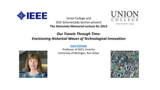
- 1. Union College and IEEE Schenectady Section present The Steinmetz Memorial Lecture for 2015 Our Travels Through Time: Envisioning Historical Waves of Technological Innovation Lynn Conway Professor of EECS, Emerita University of Michigan, Ann Arbor
- 2. A lecture in memory of Charles Proteus Steinmetz Apr 9, 1865 – Oct 26, 1923 Wiki Commons Legendary pioneer of electrical engineering, On the 150th anniversary of his birth
- 3. I’m especially honored to have been invited to give this lecture for Steinmetz has been a powerful role model for me, because of his: (i) Pivotal role in the “AC revolution”, (ii) Creatively living a wonderfully full life, (iii) And doing all this in the face of hardships that could have crushed a lesser soul. Back in 1978 at MIT, as I struggled to launch a later revolution, I kept a his photo on my office wall (see at right, just above the chair) . . . Lynn’s office at MIT, 1978
- 4. Keep these words in mind . . . “The farther backward you can look, the farther forward you can see.” – Winston Churchill Link As we travel through time . . .
- 5. We’ll first step back and reflect on some early waves of innovation Then we’ll zoom-in on the AC electricity revolution involving Steinmetz And on the later VLSI microchip design revolution that I participated in We’ll then envisioning the huge incoming wave of innovation as ever-smaller, ever-more-empowering microsystems become embedded into almost everything. Note: This slide-show (with links) will be posted online, for later reference.
- 6. Link To set the stage, let’s visualize some past waves of disruptive innovation . . .
- 7. We’ll begin in the 1400s during the Renaissance, a time of transformational cultural advances . . . Prague Astronomical Clock, c. 1410: The mechanization of astronomical calculations during the Renaissance: Photo by Hector Zenil (www.hectorzenil.net) A stunning confluence of the Mathematics, Science, Engineering Architecture and Art of the time . . .
- 8. Towards the end of the 1400’s a commingling cluster of advances in shipbuilding, navigation and map-making reached a ‘tipping point’, triggering the onset of the Age of Discovery . . . Portuguese Carrack Mariner’s Astrolabe Gimbal Compass Cantino planisphere (1502)
- 9. Charting the Early Voyages during the Age of Discovery, c.1492-1522 . . . Wiki Commons Thus it begins:
- 10. Exploration rates escalated as mass-communication by printing also spread in the late- 1400s, enabling adventurers to ever more quickly propagate news of what they’d found and how they’d found it . . . Link; Attribution: Aodhdubh at English Wikipedia Replica Gutenberg Press at the Featherbed Alley Printshop Museum:
- 11. The escalation is evidenced, a generation later, in Diogo Ribeiro’s much-more-detailed World Map as of 1527 . . . Wiki Commons
- 12. And two generations later, in Mercator’s projection-map of 1569 . . . Wiki Commons
- 13. Source By the early 1700’s, exponentiation had generated a massive global trading system . . .
- 14. Now, what’ happening here? Just exponentiation of THINGS? Is that all it is? Or exponentiation of key clusters of innovative IDEAS in the minds of ever more people? IDEAS on how to MAKE and USE things . . . Mariner’s Astrolabe Gimbal Compass Portuguese Carrack Cantino planisphere (1502) Attribution: Aodhdubh at English Wikipedia Link
- 15. By the mid-1700’s, the stage was set for a tremendous disruptive wave of technological innovation, Link and so began the industrial revolution (~1760-1850) . . .
- 16. During the Industrial Revolution the mining of coal and iron-ore was greatly amplified by steam-power . . . Snip from Google Images Some of the resulting iron was used to make more steam engines, and the positive feedback generated an iterative expansion-process . . .
- 17. Initially, heavy industrial raw materials and products were transported using the expanding canal system: Wiki CommonsLoading coal on the LehighCanal Wiki Commons
- 18. By the 1830’s, steam-powered railroads began interconnecting mines to iron-works and rail-makers, enabling more-rapid expansion of railroads . . . Snip from Google Images
- 19. These charts reveal the rapid early spread of railroading in the US . . . http://www.cprr.org/Museum/RR_Development.html#2
- 20. The expansion was accelerated by rapid spread of telegraphy in the 1850s, the effect analogous to that of printing in the age of discovery . . . (Snip from Google Images)
- 21. http://www.telegraph-history.org/ http://www.telegraph-history.org/map2.htm Map of telegraph stations in the United States, Canada and Nova Scotia, 1853
- 22. Zooming into the map of telegraph stations in 1853 . . . http://www.telegraph-history.org/map2.htm
- 23. The much expanded railroad system, as of 1860 . . . source
- 24. All that set the stage for another disruptive wave of innovation, and the Second Industrial Revolution began in the 1860s/70s . . .
- 25. The Second Industrial Revolution* was characterized by (1) the build out of railroads (2) large scale iron and steel production (3) widespread use of machinery in manufacturing (4) greatly increased use of steam power (5) use of oil (6) beginning of electricity (7) electrical communications – Wikipedia Let’s first zoom-in and follow the progress of the “build out of the railroads” from 1860 – 1890 . . .
- 26. 1860 source
- 27. 1870 source
- 28. 1880 source
- 29. 1890 source
- 30. Like compound interest, the early social-diffusion rate of such clusters of technological ideas is approximately proportional to what’s already there at any given point in time . . . source y(t) = y(0)e^rt (i.e., exponential function):
- 31. y(t) = ymax/(1+((ymax/y(0))–1))e^-rt) But as the opportunity-space fills, the diffusion rate of technological ideas slows as the cluster nears its expansion limits . . . sourceearly exponentiation later saturation (i.e., logistic function):
- 32. Let’s visualize the harnessing “electricity” by the 1890’s: Electric generators, motors and lights were being embedded in a rapidly- expanding electrically-empowered industrial, commercial and transportation infrastructure. Names such as Edison, Westinghouse, Tesla, Steinmetz and Sprague were becoming famous for roles in creating the newly-spreading technologies. And the alternating vs direct (AC vs DC) “war of the currents” was on . . . The dramatic story of that era is revealed in detail in the website, displays and resources of the Edison Tech Center here in Schenectady.
- 33. Visualizing the spread of electrification, and it’s co-evolution with the spread of electric traction subways and interurban light-rail systems . . . Motors SubwaysInterurban rail Planning the IRT, 1891 Generators
- 34. Now let’s zoom-in and look at the special role of Steinmetz in the AC revolution . . .
- 35. 1892: “Steinmetz’ experiments . . . led to his first important work, the law of hysteresis. . . . Until that time the power losses in motors, generators, transformers, and other electrically powered machines could be known only after they were built. Once Steinmetz had found the law . . . engineers could calculate and minimize losses of electric power . . . before starting the construction of such machines . . . His work was immediately recognized as a classic . . . Steinmetz’ reputation was assured at the age of 27.” Encyclopedia Brittanica:
- 36. 1893: “His second contribution was . . . a symbolic method of calculating alternating- current phenomena and in so doing simplified an extremely complicated and barely understood field so that the average engineer could work with alternating current. This accomplishment was largely responsible for the rapid progress made in the commercial introduction of alternating-current apparatus . . . The problem that Steinmetz faced was that electrical engineers were not taught enough mathematics to understand his new mathematical treatment of problems using complex numbers. 1897-1911: To educate the electrical engineering profession, he published several textbooks . . . through his writing, lecturing, and teaching*, his method of calculation with complex numbers was universally adopted in work with alternating currents.” *at Union College Encyclopedia Brittanica
- 37. Steinmetz’s symbolic mathematical methods that enabled large numbers of engineers to easily “navigate” the world of AC electricity: In doing this work, Steinmetz also pioneered in the emergence of 20th century methods in engineering science and engineering education . . .
- 40. He also masterfully unfolded the abstract mathematics behind his symbolic methods . . . Link
- 43. With the result that newly-educated electrical engineers could mechanize the resulting mathematical calculations using instruments such as this K&E 4053-3 Slide Rule, c.1910 . . . Source
- 44. Leading to a rapid build-out of AC generation and transmission infrastructure from 1900’s onwards . . . SmithsonianSmithsonian
- 45. Expanding into the vast infrastructure now used for efficiently generating and transmitting AC electric power from energy-sources to end-users . . . Snip from Goggle images
- 46. Visualizing the U.S. high-voltage AC transmission grid (as of 2008) Wiki Commons Logistic function
- 47. To envision its dramatic scale, look at the US at night, as seen from space . . . NASA Think how many minds Steinmetz’s ideas passed thru to make this happen . . .
- 48. Link 1929 Link 1992 1924 Link Readings where you can learn more about Steinmetz’s amazing life . . .
- 49. Steinmetz Digital Collection of Schenectady Working in his home laboratories . . and at Camp Mohawk . . enjoying life with his adopted family
- 50. Let’s go ‘Back to the Future’ again, and zoom-in on a later disruptive wave of innovation in electronics and computing . . . One I participated in: the revolution in Very Large Scale Integrated (VLSI) microchip design, beginning in 1976 . . .
- 51. The stage was set by emergence of integrated circuit technology in the 1960’s, enabling numbers of transistors and their wiring to be ‘printed’ onto chips of silicon . . . Some early integrated circuits: Snip from Goggle images
- 52. And by the early 70s revolution in computer design (using MSI integrated circuits): Innovation of the interactive-display, mouse-controlled “personal computer”, the “Ethernet” local-area network, and the “laser printer” (at Xerox PARC) . . . Wiki commons Xerox Alto, 1973 Metcalfe’s original Ethernet sketch, 1973 And the Dept. of Defense’s “Arpanet” (the early internet, at DARPA) . . . Arpanet map, 1971 Laser printer, 1971 Source Source
- 53. Ongoing advances in lithography enabled ever-finer features to be printed, rapidly increasing the number of transistors printable on single chips. And by 1971, a watershed was crossed with the introduction of the Intel 4004, the first single-chip “microprocessor”: a “computer processor on a chip” . . . It contained 2300 transistors . . . Source Source
- 54. Here’s a 4004’s mask set (overlain like a stack of photo negatives), showing patterns “printed” in each layer of the chip that together will create the 2300 transistors and their interconnections. This “at-the-time” complex design had to be manually drafted, without aid of computers. Each mask layer was crafted by hand-cutting its drafted pattern into a large sheet of ‘rubylith’. Sheets were then overlain to check for interlayer design- rule violations. Then each photo-reduced to make the 4004’s mask set.
- 55. Gordon Moore at Intel observed that the number of transistors reliably printed on chips was roughly doubling every two years . . . N(t)/N(0) = 2^(t/2) Moore’s Law (as of 1976) After all, looking ahead it appeared conceivable by ~1990 an entire superscalar “supercomputer” could be printed on a single chip. . . An exponential function, graphed on a vertical log scale . Carver Mead named this “Moore’s Law” and determined that there were no physical limits to increasing the density up to ~ 1 million transistors. In 1976 this set-off a push at Xerox PARC and Caltech to figure out how to enable such complex things to be designed.
- 56. For more insight into that, you can browse my “Reminiscences of the VLSI Revolution” in the Fall 2012 IEEE Solid State Circuits Magazine. Tonight we’ll just hit the highlights, including how Steinmetz’s story influenced the outcome ... The story of what unfolded over the following three/four years is quite a saga . . . That was the first time I’d come forward to tell the whole story . . .
- 57. The breakout was triggered by a cluster of abstract innovations at Xerox PARC and Caltech . . . Link Included were a set of scalable VLSI chip-layout design rules, in the form of ratioed (dimensionless) inequality equations (Conway, Xerox PARC) . . . These enabled abstract chip designs to be digitally shrunk down (and reused) as Moore’s law rapidly advanced . . . They also enabled accruing chip subsystem designs to be widely shared . . .
- 58. The driving idea: Assuming that chip lithography scales-down year by year according to Moore’s Law, And ever-more ever-faster transistors can be printed on single chips as time goes by, do: Step (i): Use a computer and the new methods to design the layout patterns for a processor of more a powerful computer, to be “printed” in the next denser process. Step( i+1): Use the new chips and new software chip-design tools to create more powerful “computer-design” computers, then repeat step (i). If ever more engineers and programmers could do this, and on an expanding number of increasingly powerful computers, then the iterative expanding-process could explosively generate ever-more and ever-more-powerful digital systems . . . (i.e., exponentiate!). The big problem: Where are all the engineers and programmers going to come from, and how are they going to learn how to do this? Aha! Recall how Steinmetz coped with this problem . . .
- 59. So, we first documented the ‘Mead-Conway’ system of simplified, restructured, design-level abstractions and chip design methods in an evolving computer-edited book . . . Link Thus we used our Alto computers to mechanize not only our computations, and our generation of chip-design layouts, but also the evolution of the book itself . . .
- 60. That computer-edited evolving book, printed using the laser printers at PARC, became the draft of the famous textbook: Introduction to VLSI Systems by Mead and Conway, published in 1980 . . .
- 61. We also used our Altos to generate (at Xerox PARC) many open-source cell-layout-designs for key digital-subsystems, easily disseminated to students and colleagues via the Arpanet … CIF 2.0 Cell-Library code PLA cells Clock drivers I/O Pads Cell locations URL
- 62. And, following the “script” Steinmetz used to propagate his revolutionary AC methods at Union College, I introduced the new methods in a special VLSI design course at MIT in 1978. Link Link Link
- 63. The students learned to design chips in the 1st half of the course, then did project-chip designs in the 2nd half. They were fabricated in Pat Castro’s lab at HP shortly after the course. There were many amazing results including a complete Lisp microprocessor design by Guy Steele . . .
- 64. Map and photomicrograph of the 19 student projects on the MIT’78 ‘MultiProject’ Chip For more about the MIT’78 course, see Lynn’s “MIT Reminiscences”
- 65. The MIT’78 course stunned top folks in Silicon Valley . . . Chip design till then had been a mystery, only grasped by a few computer architects working for chip manufacturers . . who thus had access to the “printing plants” . . . Many other top research universities wanted to offer such a course. But how? After intensive pondering, I came up with the answer: Rerun the MIT’78 course at a dozen research universities, using my MIT lecture notes to keep everything in sync. But how to “print” the student project chips? I suddenly envisioned a new form of “E-commerce” system, enabling student design files to be remotely submitted via the Arpanet to a “server” at PARC . . . The server would run logistics-software to pack the designs into multi-project chip files (like composing the print-files for a magazine, using remotely-submitted articles) . . . We’d then make masks, “print” MPC’s at HP Labs (where my collaborator Pat Castro had prototyped the first “silicon foundry”), and quickly return the chips to students.
- 66. In the fall of 1979, we orchestrated a huge “happening” (MPC79*) . . . It involved 129 budding VLSI designers taking Mead-Conway courses at 12 research universities… *The MPC Adventures, L. Conway, Xerox PARC, 1981 MPC79 Arpanet E-commerce system:
- 67. MPC79 not only provided a large-scale “demonstration-operation-validation” of the design methods, design courses, design tools and e-commerce digital-prototyping technology … it also triggered ‘cyclic gain’ in, and exponentiation of, the budding VLSI-design-ecosystem… The MPC Adventures, L.ynn Conway, Xerox PARC 1981.
- 68. Thus breaking the “VLSI complexity barrier”, spawning the MOSIS* national chip-prototyping service, and bootstrapping the “fabless-design + silicon foundry” paradigm of chip-making … *By transfer of MPC79 technology from Xerox PARC to USC-ISI Lynn and her team prepare packaged chips to send to designers, Jan 4, 1980 MPC79: Wafer . . . . . Chip . . . . . . . Packaged Chip . . Example: Jim Clark’s “Geometry Engine”
- 69. Visualizing how techno-social dynamics triggered an exponentiation in the spread of the innovative VLSI design ideas via the emerging internet communication technology . . . The MPC Adventures (p. 16) By 1982-83, Mead-Conway VLSI design courses were being offered at 113 universities all around the world
- 70. Starting with several thousand in 1971, by 2011 the number of transistors on a chip had passed several billion! In parallel with all that, over the past 40 years or so, we’ve see Moore’s Law stay on track all the way! N(t)/N(0) = 2^(t/2) N N(0), t(0) (exponential function with t in years) (exponential function graphed on log scale)
- 71. Here’s a partial map of the Internet . . . Zooming in to see IP Addresses . . . Wiki Commons Visualizing the Internet’s expansion by 2010 . . .
- 72. Global Foundries VLSI silicon-chip fabrication plant, Malta, NY . . . Panoramio, Google MapsA giant “printing plant” for patterning complex microsystems onto vast numbers of silicon chips . . . And Under Construction, June 26, 2014!
- 73. And here are the top “Silicon Foundries,” as of 2013: These are where many of the world’s VLSI silicon microchips are “printed” . . . Wikipedia
- 74. Taking a glimpse inside the huge TSMC foundry in Taiwan . . . Google Images
- 75. The microchip designs are being created by engineers in companies all around the world, then sent via the internet to such “foundries” for “printing” . . . In effect, turning “Sand” (which is mostly SiO2) into “Gold”. . . !
- 76. The resulting VLSI chips are then used by design engineers to functionally empower and control all sorts of things . . . things that they’re deeply embedded into . . . Smartphones Wearables Autos Drones Snips from Google Images
- 77. Zooming in on one example, here we see an iPhone 5 chip with Dual ARM Cores and multiple GPUs
- 78. Link Interactive Zoom-in Internet Map, 2015 This also includes chips that empower the internet . . . exponential function which continues to expand exponentially . . .
- 79. NASA: Earth from space at night With the internet connecting ever-more-people and chip-empowered-things, just imagine what’s going on out there, right now, all around the world! Thus setting the stage for what’s coming next . . . !
- 80. To learn more about the social, technological and human drama surrounding the remarkable birth of personal computing and the internet, see these books: LinkLinkLink 201019991999
- 81. Link "What's past is prologue" – William Shakespeare It’s now time to look forward, into the future . . . !
- 82. wave of innovation out there, now just beyond the social-time-horizon . . . As we turn 180⁰ and look ahead . . . we can visualize a huge incoming
- 83. One thing for sure: Link This one is the “Big One”! . . .
- 84. Up until now microsystems have been deeply embedded out-of-sight and out-of-mind inside of “things” like . . . Smartphones Wearables Autos Drones But why is it starting now? . . . Let’s set the stage:
- 85. Thus few folks visualize the “many ideas in motion” that generate the astonishing ‘out-of-body’ experiences when flying a Parrot Bebop with an Oculus Rift. . . www.youtube.com/watch?v=6ZdSMAG90Rs www.youtube.com/watch?v=Io6V0NR7DN0
- 86. That’s all about to change due to technological milestones such as Motorola's "Project Ara" to create modular smartphones . . .
- 87. Ara’s ‘Phonebloks’ will popularize the concept of micro ‘Hardware Apps’ Many far-tinier than current-day ‘big things” like cameras, GPS units, servos, bluetooth links, microphones . . . Such microsystems now in our smartphones (but out of sight and out of mind) will suddenly become more visible. And they’re not just processor chips, they’re also Micro Electro Mechanical (MEMS) Chips, tiny micro-mechanisms also printed lithographically in “foundries”. . .
- 88. MEMS, such as inertial measurement units (IMUs), microsensors, microcams and micro-transducers . . . and their microcontrollers and micro-interconnects . . . IMUs Microcameras Sensors Interconnects
- 89. And they’re all getting a LOT tinier! See for example: The Michigan Micro Mote: “ . . . researchers at the University of Michigan under the direction of Professors David Blaauw, Dennis Sylvester, David Wentzlof and Prabal Dutta have recently announced the . . . “Michigan Micro Mote.” . . . a multi-layered integrated circuit with built-in solar cells, battery, microprocessor, sensors, radio and memory . . . come(s) in three types, measuring temperature, pressure or images“ Computer History Museum
- 90. To glimpse where this is heading, check out the Zano drone, a recently launched “animated system” … Extremely tiny, it includes an HD cam, IMU, GPS, MCU, IR obstacle avoidance, gesture control, auto following, swarming and more… There are so many dimensions to its capabilities, it’s hard to even say where the “system” begins and where it ends . . . check out this amazing VIDEO! Source https://www.youtube.com/watch?v=hgkbhjXTbOE
- 91. These aren’t just frivolous recreational play-things, but instead have vast potential for human empowerment . . . Consider the story of a heart-patient confined by an lengthy hospital stay He can now enjoy exploring the beautiful world outside his window, a laptop controlling his drone, providing stunning views of what’s out there It won’t be long before we can join friends on group “drone-tours” of remote places around the world, right from own individual homes . . . With each our drones “carrying our eyes” remotely in the form of fisheye lenses and microcams (as in the Bebop) Which we see through by using our Oculus Rifts over the internet!
- 92. Imagine the impact as today’s kids start peeking at the insides of Zano nanodrones! URL Think of the possibilities of what they might do next!
- 93. Some ideas/things in the coming wave of innovations are hinted-at by the new Myo gesture control armbands from the mechatronics engineers at Thalmic Labs: https://www.thalmic.com/en/myo/ VIDEO VIDEO VIDEO VIDEO!
- 94. So, what’s happening here? Instead of just printing a billion transistors onto single “large” smartphone chips. We can also print a million transistors onto 1000 very tiny but very powerful chips. I.e., you can actually do a lot with a million transistors! So we can now embed lots and lots of tiny micro-processors and MEMS micro- mechanisms into almost everything. Placing them were they can get local physical data such as position, acceleration, temperature, pressure, etc. Thus enabling smart-distributed-clusters of tiny chips to animate and interactively control many macro-scale systems such as robots, drones, autos . . .
- 95. Such chips can be selected and embedded in macro-scale systems By exploiting innovations in selection methods, and innovations in woven, printed, near-field and wireless interconnections . . . Micro Chiplets (XeroxPARC) Low-energy Bluetooth beacons Smart textiles (PASTA) Near-field communications Video
- 96. This embedded-microsystems revolution is getting up a big head of steam in emerging “Silicon Valleys”, “Cambridges” and “Maker Valley’s” all around the world …
- 97. Source We can zoom-in and watch it unfold in mappings of many specific areas of micro-system technology, such as the image sensors for “microcameras” . . .
- 98. And in the movement of “application-idea-clusters” along Gartner’s “Hype Cycle” 2014 URL
- 99. One key cluster of innovations on that wave is “3D Printing”. . . Enabling macro-scale 3D “things” to be quickly made from digital-specs created by designers using personal computers . . .
- 100. 3D printers enable making prototype macrostructures such as robots, drones, medical devices, and more . . . into which microsystems can be embedded . . . Once prototypes are perfected, design-files can be shared or marketed to other 3D printer users anywhere . . . When those “things” become obsolete, their polymer macro-structures can be ‘melted-down’ and reused to make new “things” . . .
- 101. Innovative new micro-hardware apps can also be inserted into such additive manufacturing systems . . . enabling a 3D printer that print 3D printers* to prototype a yet more powerful 3-D printer! *“Printers for Pearce: An Interview with 3D Printers for Peace’s Dr. Joshua Pearce”, Michael Molitch-Hou, 3D Printing Industry, 10/18/13 See also: http://www.youtube.com/watch?v=C8Wv3LCJcUE and http://www.youtube.com/watch?v=yiJDx9dCfEQ Just as when some of the iron was fed-back to make more steam engines to further empower the industrial revolution . . . Innovating such iterative feedback loops yields “gain” in the technological exploration system . . .
- 102. ‘Blended Learning’ by giulia.forsythe, Flickr‘What is a MOOC?’ by giulia.forsythe, Flickr But (recalling Steinmetz’s dilemma) how will all the young innovators learn to grasp the new wave of concepts propelling this revolution? Fortunately, a wave of exploratory change is sweeping engineering education, just in time . . .
- 103. And more . . . Source
- 104. Many young incoming engineering students have also gained deep-experiences at. . . LEGO Camps Maker Faires FAB Labs Robot Competitions
- 105. Plus, they can now gain ongoing knowledge as needed, using internet-based lifelong-learning resources . . .
- 106. Some (the “microsystems designers”) will go on to exploit rapidly-evolving electronic design automation (EDA) and “multi-physics” design tools to create new micro-hardware apps . . . Snip from Google Images
- 107. Exploiting innovations such as 3D chip-stacking and through-silicon vias (TSVs) to compose ever-tiner chip-modules and “hardware Apps” (like the ‘Micro Mote’) . . .
- 108. Many others (the “mechatronics designers”) will use collaborative macro-scale design tools such as Dessault Systems’ ‘3D Experience Platform’ to innovatively embed smart modular hardware-apps to dramatically animate a new wave of human- scale systems . . . https://www.youtube.com/watch?v=IPu28vUcZzI
- 109. Starting within cars World-wide automotive technology will be a huge driver of the rapid embedding of micro-hardware Apps into human-scale systems. . . and on into Mobility technology and into Smart Roadways
- 110. Now we’ve all heard about Self-driving cars . . .LA Times Infographic:
- 111. For example, just this week at the Shanghai Motor Show (April 20-29, 2015) Mini is showcasing their new augmented-reality glasses concept . . . To visualize the many possibilities of this concept, watch this remarkable VIDEO But what about exploiting “Augmented Reality” (as in “Parrot Bebop + Oculus Rift”) in conjunction with mobility technology . . . http://traffictechnologytoday.com/news.php?NewsID=68125
- 112. VIDEO: Approaching the Mini . . . Seeing through the side-doors . . . Deciding where to go next . . .Seeing real wheel when parking . . . https://www.youtube.com/watch?v=QARt89_6Jrs#t=19
- 113. http://blogs.jabil.com/2014/08/13/internet-of-things-infographic/ The innovative embedding of ever-tiner micro-hardware apps will quickly spread . . .
- 114. http://blogs.jabil.com/2014/08/13/internet-of-things-infographic/ And begin to functionally enhance just about everything . . .
- 115. Along the way, the microsystem supply-chains into the electronics, automotive, medical, clothing, home-appliance and building industries will cross-couple and commingle Source and enhancements gained in each will quickly cross-fertilize others . . .
- 116. There will be many disruptive changes in current business models such as . . . Reshorings will reduce clustered turnaround times . . . Order-to-Delivery times pace rates of exploration . . . Logistics systems will take center stage . . . SourceSource
- 117. From: The Age of Opportunity: Harnessing Complexity To Solve Big World Problems by Frank Spencer, kedgefutures.com But how will we cope with the ‘complexity’ of the emerging techno-social ecosystem?
- 118. By exploiting things like collaborative learning, crowdsourcing, crowdfunding, IP brokering, agile methods, rapid-digital-prototyping, and more . . . Everyone, from engaged-users to makers, will be able to scale up their participation and impact.
- 119. NASA Only now, instead of just exploring how to make ever bigger things that go ever further and ever faster, such as when reaching for “outer space”. . .
- 120. We’ve inverted our perspective 180⁰, reaching down into the “deep inner spaces” of the micro/nano/pico world . . . And are exploring how to make and exploit vast-quantities of ever-tinier, ever-more-empowering “micro/nano things” . . . Google Images
- 121. For example, using Scanning Electron Microscopy (SEM) to study the details of the tiny micro-machinery printed on MEMS chips . . .
- 122. Atomic Force Microscopy (AFM) Scanning Tunneling Microscopy (STM) And zooming-in even further to measure and maps things down at the molecular and atomic levels . . . So as to guide adventurers on explorations at places and in fields such as . . .
- 123. MIT Nano Harvard Wyss Institute DARPA Microsystems Synthetic Biology Biologically Inspired EngineeringModel-Based Design STEM + ARTS = STEAM Draper Lab Collaboration Technology Augmented Reality Social Media Genetic Algorithms Self Assembling Systems Google ATAP Microsoft Research Facebook Research Universities Machine Vision Machine Hearing Augmented Kinesthetics Social Physics Social Dynamics Social Machines Social Learning Multiengineering Meta^2Mathematics MetaArchitecture UPS AmazonExploration Infrastructure
- 124. Thus it begins, all around the world . . .
- 125. Link And it’s on its way . . . !
- 126. Before long, adventurers around the world will be “surfing” somewhere on this wave . . .!
- 127. Ah, but the escalating rates of techno- social-change will challenge existing cultural patterns, because of massive social accumulations of past habits: What’s the new game this time? Who gets to play? What rules do we play by? Where can we turn for guidance? And how do we drop old habits? . . . URL
- 128. For insight into what's about to happen, reflect on this news: 'Apple Watch designers on easing the smartphone tyranny they created' http://www.wired.com/2015/04/the-apple-watch/ It will help you to "Remember, this bold step into the future is NOT about "the things", it's about the creative "IDEAS and VISION embodied in the things“. – Lynn Conway
- 129. But you say, “how can we ever keep up?” Hasn’t the train already left the station, for many of us? Some words to remember: "In a world of change, the learners shall inherit the earth, while the learned shall find themselves perfectly suited for a world that no longer exists" – Eric Hoffer And it’s ever-easier to engage in fun-filled, lifelong learning . . . Besides, “As the rate of techno-social change increases, we’ll all live far further into the unfolding future than we ever dared dream“ – Lynn Conway
- 130. The MPC Adventures (p. 16) Xerox PARC 1981. URL When visualizing these swirling masses of ideas in motion reflect back on the rapid-evolutionary-process-diagram from the VLSI revolution . . . Only now, vastly more such processes run in parallel and cross-fertilize . . . While a new science explores, maps and describes what’s happening . . .
- 131. 1976 1978 1979 ’79: Launching the VLSI courses via MPC79!! 1977 ’76: How to cope with VLSI complexity? ’77: Inventing scalable VLSI design rules. ’78: Launching the VLSI methods at MIT! Visualizing the exponentiating wave of VLSI innovation . . .
- 132. Some questions to ponder as we begin surfing such waves: How do we gear-up and learn the basic moves? Who do we team-up with and where do we go exploring? Where is this thing headed and what’s our mission? unfolding exponentiation nearing saturation Of course such 2D views miss lots of what’s happening . . . Let’s play with visualizing waves in 4D to gain a better perspective . . .
- 133. Is this a Traveling Wave? A Standing Wave? Or What? This stunning video* hints at ways to think about it . . . Lets playfully visualize the incoming wave of innovation as a time series of “GHC profiles” (2D slices thru the 3D wave at increments in time) . . . *"Water," by Morgan Maasen http://vimeo.com/90429499 Gartner Hype Cycle 2014 http://www.gartner.com/newsroom/id/2819918
- 134. Finally, some conjectures about possible futures: By cooperatively learning and sharing ideas on how to do more-and-more with less- and-less, the incoming wave of innovations has the stunning potential of: (1) Sustainably providing ever-increasing infrastructural functionality and life empowerment per person, (2) While consuming ever-decreasing energy and material resources per person (3) Thus beginning the reigning-in of our unsustainable over-use of planet earth (4) While simultaneously opening an unprecedented collaborative/competitive exploration of the greatest of frontiers, the frontier of “What it’s possible to do”!
- 135. . . . and a personal perspective on “Our Travels Through Time”. . . “If you want to change the future, start living as if you’re already there!” – Lynn Conway Source
- 136. END Link to Epilogue, References, Notes & Afterwords