1. Introduction
Introduction
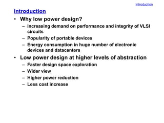
• Why low power design?
– Increasing demand on performance and integrity of VLSI
circuits
– Popularity of portable devices
– Energy consumption in huge number of electronic
devices and datacenters
• Low power design at higher levels of abstraction
– Faster design space exploration
– Wider view
– Higher power reduction
– Less cost increase
2. Introduction
– Opportunities for power reduction at every level of
abstraction
System 50-90%
algorithms, HW-SW tradeoffs,
supply voltage scaling, bus encoding
Architecture 40-70%
scheduling, resource binding,
operand swapping
Register-
Transfer
30-50%
clock gating, operand isolation,
pre-computation,
dynamic operand interchange,
FSM encoding
Gate/Logic 20-30%
technology mapping,
don’t care optimization,
de-glitching
Transistor 10-20%
transistor sizing
Physical 5-10%
interconnect capacitance reduction,
clock-tree synthesis
3. Introduction
– Power dissipation in CMOS circuits
• Dynamic power dissipation (dominant)
• Short-circuit power dissipation
• Leakage power dissipation
– Dynamic power dissipation
: effective (switched) capacitance
: clock frequency
: switching activity
: supply voltage
: physical capacitance
P C V f
C V f
dynamic eff dd
2
clk
phy dd
2
clk
=
= a
fclk
Vdd
Ceff
a
Cphy
4. Physical/Transistor/Gate-Level Design
Physical/Transistor/Gate-Level Design
• Interconnect capacitance reduction
– Signals having high switching activity are assigned
short wires
• Clock-tree synthesis
– Clock is a major source of dynamic power dissipation
– Clock of 200MHz DEC Alpha chip drives 3,250pF load,
3.3V supply voltage => 7W (30% of the total power)
– Clock skews must be controlled within tolerable values
Single driver scheme Distributed buffers scheme
(preferred)
5. Physical/Transistor/Gate-Level Design
• Transistor sizing
– Compute the slack at each gate
– Sizes of the transistors in the gate are reduced until the
slack becomes zero
– Reduced size => reduced capacitance => reduced power
– Critical path is not affected
– Path balancing => reduced glitch => reduced power
6. Physical/Transistor/Gate-Level Design
• Technology mapping
– V. Tiwari, P. Ashar, and S. Malik, “Technology mapping
for low power,” Proc. of Design Automation Conference,
pp. 74-79, June 1993
– Hide nodes with high switching activity inside the gates
where they drive smaller load capacitances
H
L
H
L
H
L
H
L
L
L
7. Physical/Transistor/Gate-Level Design
• De-glitching
– Glitch consumes 10% - 40% of the dynamic power in
typical combinational logic circuits
– Path balancing
• Add unit-delay buffers selectively such that the delays of
all paths can be made equal
FA FA FA FA
A0
B0
A1
B1
A2
B2
A3
B3
C0
S0
C1
S1
C2
S2
C3
S3
C4
1 1
0 0
0
1
0
1
0
1
0
1
1
8. RTL Design
RTL Design
• Clock gating
– Disable clocks to idle part of the circuit
– Saves clock power and power consumed by registered
value change
register
MUX
combinational
logic
register
F/F
data
clock
control
0
1
9. RTL Design
• Operand isolation
– Exploit output don’t cares of large circuit blocks in
unused clock cycles
– Insert latches before the circuit blocks to reduce circuit
activity
register
MUX
combinational
logic
register
F/F
clock
control
0
1
multiplier
latch
adder
12. Architecture-Level Design
Architecture-Level Design
• Supply voltage reduction
– Quadratic effect of voltage scaling on power
5V --> 3.3V => 60% power reduction
– Supply voltage reduction => increased latency
P C V f
dynamic eff dd
2
clk
=
energy delay
Vdd Vdd
5
1 5
1
a
)
( th
d
g
V
V
V
K
T
=
E C V
dynamic/cycle eff dd
2
=
13. Architecture-Level Design
– Perform optimizing transformation to meet throughput
constraint even with voltage reduction
– Concurrency increasing transformation (increased
hardware cost ) => critical path reduction
– Loop unrolling, pipelining, retiming, algebraic
transformation, module selection
• A.P. Chandrakasan, M. Potkonjak, R. Mehra, J. Rabaey, and
R.W. Brodersen, “Optimizing power using transformation,”
IEEE Tr. on CAD/ICAS, pp. 12-31, Jan. 1995
– YN=AYN-1+XN --> YN=A2YN-2+AXN-1+XN
YN-1=AYN-2+XN-1 YN-1=AYN-2+XN-1
+
*
D
XN YN
A
+
*
2D
XN YN
A2 *
+ YN-1
+
*
A
YN-2
XN-1
A
14. Architecture-Level Design
+
*
D
XN YN
A
+
*
2D
XN YN
A2 *
+ YN-1
+
*
A
YN-2
XN-1
A
Ceff=1
Voltage=5
Throughput=1
Power=25
Ceff=1.5
Voltage=3.7
Throughput=1
Power=20
+
*
2D
XN YN
A2 *
+ YN-1
+
*
A
YN-2
XN-1
A
Ceff=1.5
Voltage=2.9
Throughput=1
Power=12.5
D
D
15. Architecture-Level Design
• Reduction of effective capacitance
– R. Mehra, L.M. Guerra, and J.M. Rabaey, “Low power
architectural synthesis and the impact of exploiting
locality,” Journal of VLSI Signal Processing, 1996
– Buses consume 5-40% of the total power
– Reducing access to global resource thru clustering
+ +
+ +
+ +
+ +
+ +
+ +
+ +
+ +
Global data transfers
Local data transfers
+
+
Adder1
Adder2
16. Architecture-Level Design
• Switching activity reduction
– Increasing data correlation thru operand sharing
• Operations sharing an operand also share resource
• Actively increase the chance of operand sharing thru loop
interchange, operand reordering, loop unrolling, loop
folding
– Loop interchange
for i
for j
for k
for l
a=f(k, l)
b=f(i, j, k, l)
c(i, j) = a - b
for k
for l
a=f(k, l)
for i
for j
b=f(i, j, k, l)
c(i, j) = a - b
17. Architecture-Level Design
– Scheduling and binding
• E. Musoll and J. Cortadella, “Scheduling and resource binding for
low power,” Proc. of Int’l Symp. on System Synthesis, pp. 104-109,
Apr. 1995
• Resource sharing by sibling operations
• Operations sharing the same operand are scheduled in control
steps as close as possible (higher priority is given for list
scheduling)
• After functional unit binding, bind registers such that useless
power is reduced (no change of inputs to idle functional unit)
*
*
*
n1 n2
n3
n4
*
*
n5
*
*
*
n1 n2
n3
n4
*
*
n5
traditional modified
*
*
* idle
19. Bus Encoding
Bus Encoding
• Reduce number of transitions on high-
capacitance, multi-bit buses by encoding the
signals
• Example
– Bus-invert coding
• M.R. Stan, W.P. Burleson, “Bus-invert coding for low-power
I/O,” IEEE Trans. on VLSI Systems, Vol. 3, No. 1, pp. 49-58,
Mar. 1995
high-capacitance
00110001
01001100
00110001 0
10110011 1
6 toggles
3 toggles
20. shutdown
Dynamic Voltage Scaling
Dynamic Voltage Scaling
a
)
( th
d
g
V
V
V
K
T
=
Dynamic power dissipation
clk
dd
eff
dynamic f
V
C
P 2
=
Gate delay by a power model
Energy per cycle
2
_ dd
eff
cycle
per V
C
E =
Energy consumed by a task that takes n cycles
n
V
C
E dd
eff
task
2
=
V
V
V
K
f th
f
clk
a
)
(
=
not a function of time but a function of # cycles (switchings)
performance
0 deadline
n
V
C
E dd
eff
task
2
=
n
V
C
E dd
eff
task
4
2
=
2
,
2
clk
dd
f
V
1
, clk
dd f
V
full speed
low speed
21. Dynamic Voltage Scaling
• DVS on a Microprocessor System
– T. Pering, T., and R. Brodersen, “Dynamic Voltage
Scaling and the Design of a Low-Power Microprocessor
System,” in Power Driven Microarchitecture Workshop
in conjunction with ISCA98, June 1998
– System block diagram (ARM8 architecture)
mProc.
Core
I/O bridge
SRAM
Unified
Cache
DVS components
Fixed-voltage
components
SRAM
SRAM SRAM
22. Dynamic Voltage Scaling
– System energy breakdown
Core
58%
Processor Bus
7%
Cache
33%
SRAM
2%
Benchmark
Miss
Rate
Idle
Time
Bus
Activity
AUDIO 0.23% 67% 0.35%
MPEG 1.7% 22% 14%
UI 0.62% 95% 0.52%
23. Real-Time Scheduling on a VSP
Real-Time Scheduling on a VSP
• Y. Shin and K. Choi, “Power conscious fixed
priority scheduling for hard real-time systems,”
Proc. of Design Automation Conf., pp. 134-139,
June 1999
• Two methods for power reduction in processors
– Power-down mode
– VSP (Variable Speed Processor)
– Proposed method:
• Combine the two methods to obtain power saving for real-
time systems
• Exploit execution time variation and idle interval
How to exploit these features ?
Scheduling
24. Real-Time Scheduling on a VSP
• Priority-based preemptive scheduling
– Simple to implement
– Many analytical methods for schedulability analysis
– Fixed (static) priority (RMS, DMS) LPFPS (Low Power
Fixed Priority Scheduling)
– Dynamic priority LPEDF
• Implementation of priority-based preemptive
scheduling
– Active task, Run Q, Delay Q
25. Real-Time Scheduling on a VSP
Active task
Run Q
Delay Q
0 100 200 300
Run Q is empty
The speed of the processor can
be slowed down until time 200,
which is min(deadline of ,
next arrival time of Delay Q.head)
26. Real-Time Scheduling on a VSP
0 100 200 300
BCET/WCET
0.0
0.1
0.2
0.3
0.4
0.5
0.6
0.7
0.8
0.9
1.0
3D-image
diesel
fft
bsort
smooth
blue
check-
data
whetstone
line
The chance for speed control increases
as the variation of execution time increases.
Variation of execution time [Ernst 97]
27. Real-Time Scheduling on a VSP
0 100 200 300
Active task
Run Q
Delay Q
Active task
Run Q
Delay Q
Next arrival time of Delay Q.head
We can bring the processor
into the power-down mode
because the processor will
be idle until time 200
All the tasks reside in the Delay Q
28. Real-Time Scheduling on a VSP
– VSP
• NOP: 20% power consumption compared to typical
instructions
• Power-down mode: 5% power consumption of fully active
mode with 10 cycles delay
• Frequency: 100 MHz to 8 MHz with 1 MHz step
• Voltage: 3.3 V to 1.1 V
– Experimental procedure
• Control BCET: 0.1*WCET ~ 1.0*WCET
• Execution time: random variable following Normal
distribution with m=(BCET+WCET)/2, =(WCET-BCET)/6
• Run 3 times for each method and take average