The 10 most disruptive companies in semiconductor industry compressed
•
0 likes•101 views

Semiconductor chips power technologies to enrich people's lives by assisting several businesses in running faster, smarter, and with increased operational efficiencies.

Recommended
More Related Content
What's hot
What's hot (9)
Similar to The 10 most disruptive companies in semiconductor industry compressed
Similar to The 10 most disruptive companies in semiconductor industry compressed (20)
More from Insights success media and technology pvt ltd
More from Insights success media and technology pvt ltd (20)
Recently uploaded
Recently uploaded (20)
The 10 most disruptive companies in semiconductor industry compressed
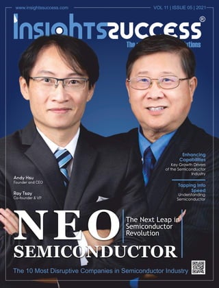
- 1. www.insightssuccess.com VOL 11 | ISSUE 05 | 2021 Tapping Into Speed Understanding Semiconductor Enhancing Capabilities Key Growth Drivers of the Semiconductor Industry
- 4. Achieving Leading-Edge Capabilities he semiconductor industry plays a heroic narrative, Tcarrying innovative technological developments on its back while tackling the current challenges. It plays a vital role by providing various chips that are the absolute pinnacle pillar of all technological developments in the ever-evolving digital world. Pioneering companies in the semiconductor industry are constantly trying to achieve leading-edge capabilities by creating advanced semiconductor chips with increased memory capacity and more incredible computational abilities that will help take the revolution of digitalization to the next level. The vast applications of these chips are widespread in various industries, upscaling the utilization to assist various components maximizing the capabilities to speed up the processes at a never before seen pace. Semiconductor chips power technologies to enrich people's lives by assisting several businesses in running faster, smarter, and with increased operational efficiencies. With the pandemic disrupting the semiconductor industry globally, creating a significant shortage of chips, semiconductor companies prioritize achieving design and manufacturing capacities to tackle this issue head-on. These companies intend to develop solid capabilities chips to aid the supply chain, research, intellectual property protection, and navigating policies for designing and manufacturing highly capable semiconductor chips. Resolving construction issues, moderating equipment costs, and enhancing internal capabilities can help semiconductor companies attain manufacturing excellence for building chips that give a strong performance with low power consumption can create the maximum impact in the industry. The advanced semiconductor chips are the brain behind modern electronics, and all the modern system runs with these advanced chips. Editor’s Desk
- 5. What oxygen is to humans is what semiconductor is to modern electronic products. The more advanced the semiconductor chips, the more capabilities they can provide. The semiconductor companies can create more modern products with advanced semiconductor chips that consumers will enjoy with greater computational abilities and enhanced memory into contemporary electronic products. Such companies can disrupt the semiconductor industry to a great extent by creating products with leading-edge capacities. Semiconductor chips are the essential thing that the world has ever known since they are the brain behind powering modern technologies. Semiconductor companies are creating world-changing disruptions by providing various industries from Artificial Intelligence, automation, space tourism, genomics medicine, electronics by designing and manufacturing the most advanced semiconductor chips. Insights Success started a voyage to find "The 10 Most Disruptive Companies in Semiconductor Industry." This edition will take you through the impeccable testaments these companies have achieved over the years and boldly engrave their name in the industry. While flipping through pages, have a glance at the articles written by our in-house editorial team. Enjoy the read! sharad@insightssuccess.com Sharad Chitalkar
- 6. Cover Story NEO Semiconductor The Next Leap in Semiconductor Revolution 08 Articles Enhancing Capabilities Key Growth Drivers of the Semiconductor Industry 20 Tapping Into Speed Understanding Semiconductor 32 Agile Analog Analog IP the Way You Want It 16
- 7. Ambiq Endpoint Intelligence 24 Diakopto Game-changing EDA Solutions 28 Efinix Providing High Performance and Reconfigurable FPGAs for Meeting Computing Demands of Mainstream Applications 34 Omega Optics Connecting the World 40 C O N T E N T S
- 8. sales@insightssuccess.com November, 2021 Editor-in-Chief Senior Sales Manager Business Development Manager Marketing Manager Technical Head Technical Specialist Digital Marketing Manager Research Analyst Database Management Technology Consultant Hitesh Dhamani Managing Editor Anish Miller Executive Editor Sharad Chitalkar Assistant Editors Jenny Fernandes Visualizer David King Art & Design Director Priyanka Rajage Associate Designer Kartik Balapurkar Kshitij S Peter Collins John Matthew Sales Executives David, Martin, Maneesh Business Development Executives Steve, Joe, Sanket Jacob Smile Aditya Marry D'Souza SME-SMO Executive Amol Wadekar Frank Adams Circulation Manager Robert Brown Stella Andrew David Stokes Shubham Dali Co-designer Copyright © 2021 Insights Success, All rights reserved. The content and images used in this magazine should not be reproduced or transmitted in any form or by any means, electronic, mechanical, photocopying, recording or otherwise, without prior permission from Insights Success. Reprint rights remain solely with Insights Success. Follow us on : www.facebook.com/insightssuccess/ www.twitter.com/insightssuccess We are also available on :
- 9. Brief Company Name Jensen Huang Founder NVIDIA nvidia.com NVIDIA’s invention of the GPU in 1999 sparked the growth of the PC gaming market, redefined modern computer graphics, and revolutionized parallel computing. Pete Hutton Executive Chairman Agile Analog agileanalog.com Agile Analog is missioned to transform the landscape of the Analog IP market space. NEO Semiconductor neosemic.com Andy Hsu Founder and CEO NEO Semiconductor is a startup company focused on 3D NAND flash memory technology. Diakopto diakopto.com Maxim Ershov CEO CTO and Co-founder Diakopto is a rapidly growing startup developing revolutionary EDA software platform, tools and methodologies. Ray Chen Founder Omega Optics omegaoptics.com Omega Optics has developed a family of high performance, reliable, low-cost and portable products for various applications in optical sensing, bio-sensing, and optical communications. Nova novami.com Zohar Gil Chief Marketing and Business Development Officer Nova delivers continuous innovation by providing advanced metrology solutions for the semiconductor manufacturing industry. Ambiq Micro ambiq.com Fumihide Esaka Chairman and CEO Ambiq was founded on the simple yet powerful notion that extremely low-power semiconductors are the key to the future of electronics. Applied Materials appliedmaterials.com Michael Sullivan Corporate VP Applied Materials is the leader in materials engineering solutions. SEMINEX seminex.com Daniel Chu VP of Marketing and Business Development SemiNex Corporation manufactures high power, infrared laser diodes for military, industrial, cosmetic and medical applications. Efinix efinixinc.com Efinix' mission is to drive the future of edge computing with its FPGA silicon platforms. Sammy Cheung Co-Founder, President and CEO Featured Person
- 12. s a business leader, one might scoff at the thought Aof inspiration in leadership. Some business leaders may dismiss the vision as over-the-top, and perhaps even pretentious. But, the world of innovation, creating wealth, great professional bonds can all be a little jarring. Without inspiration to drive a natural sense of curiosity and aspiration – the rail of productivity can quickly lose steam. On the other hand, there is a concrete way to step forward, to build, and to deliver inspiration. A company that encapsulates the spirit of inspiration at every step is NEO Semiconductor. A Game-Changing Innovation Soon after its beginning in San Jose, California in 2012, the company dedicated in 3D NAND flash memory technology and, after six years of development, devised its signature X- NAND architecture for semiconductor chips. The architecture has become a benchmark for excellence in the semiconductor industry. The award-winning architecture solves the key issue of speed and lack of adaptation in old semiconductor chips. Today, the X-NAND architecture improves random read and write speeds by 3 times, sequential write speeds by 15 times, and sequential read speeds by 30 times. This is the benchmark of excellence at NEO Semiconductor in a nutshell. NEO Semiconductor creates solutions to some of the most pressing technology issues of our time. NEO Semiconductor focuses on developing fundamentally game- changing technology. Once it has achieved this goal, it offers the technology to the world at large. Its clients stand to win by applying their IP patents to some remarkable challenges that are at the forefront of commercial investments. However, it isn’t just the commercial promise of its application that makes the company stand out among its competitors.
- 13. The X-NAND architecture solves the core issue of flexibility and adaptability in semiconductor chips. Major technology giants like Microsoft, Amazon, Google are pushing chip manufacturers to create AI-enabled chips. These chips need to access massive data and AI algorithm stored in high-speed emerging memory chips. These memory chips are likely to be tremendously expensive, and their potential adaptation to millions of upcoming AI function remains a worry. On the other hand, the X-NAND simply offers new architecture to drastically increase the performance of NAND flash memory for single-level cell, multi-level cell, triple-level cell, and quad-level cells. Its adaptation to various different cell levels enables it to offer data storage systems in key futurist applications like AI, IoT, and cloud. According to Andy Hsu, the Founder and CEO of NEO Semiconductor, “the architecture offers a high-speed, high-density, low cost, low risk, fast-turnaround solution for NAND flash memory”. A Prospect of Stability in Global Supply Chains The semiconductor industry is on the verge of a major leap in terms of technology. On the one hand, the issues with speed, adaptability, and upcoming AI applications remain key challenges for the semiconductor business. This has resulted in major supply chain delays across the globe, resulting in increased costs and disruptions in cross- industry collaboration. On the other hand, AI applications promise a new arena of opportunities for the semiconductor which transcend beyond some wild theories on commercial prospects. For example, semiconductor chips are likely to be introduced in new automated vehicles, and every other AI-driven future application, including refrigerators, smartphones, IoT, virtual personal assistants, and more. These all rely on high-speed processing of huge amount of data stored in memory chips. However, the technology to make the leap is missing. NEO Semiconductor’s signature X-NAND architecture promises to solve the supply disruption in the high-speed data storage industry. The supply chain disruption has partially come to the fore due to increased demand from clients to upgrade NAND flash memory. This is critical for the growing need to improve data storage for a wide range of machine learning, and AI applications. However, solving this challenge is not straightforward. For example, while upgrading traditional memory modules to emerging memories like FRAM, PCM, RRAM, requires new processes, and new materials. On the other hand, the X-NAND architecture does not require clients to invest in new technology, and can be directly applied to the old technology. Hence, companies can integrate X-NAND technology in their existing AI-enabled NAND flash memory framework to build the next product without any additional costs, research, or delays. An Inspirational Journey In 2020, NEO Semiconductor was awarded the ‘Most Innovative Flash Memory Startup’Award at the Flash Memory Summit. Its CEO believes NEO Semiconductor will continue to scale new heights, thanks to the growing backbone of its expertise in the 3D flash chip arena. Today, the company is solving a wide range of challenges in the semiconductor industry, including resistive memory, AI chip technology, ultra-low power CMOS-based IoT memory, and phase-change memory. Andy notes that these are key to embracing an increasingly mobile workforce. “As the pandemic raged on, everything in-between working, education, gaming, social interactions became virtual.” This has sparked a tremendous demand for faster, and higher density NAND flash memory systems. NEO Semiconductor is ready to tackle the growing challenge of competition head-on with its signature technology. The company plans to offer a customized solution to key business arenas like cloud, and data centers with specialized solutions. NEO Semiconductor will provide TLC-QLC
- 14. products for data centers, and cloud providers. Moreover, it will offer SLC- MLC products for mid-stream applications such as Storage Class Memory or SCM. For down-stream applications such as embedded systems, the company will offer serial NAND flash memory. The strategic and wise planning will likely ensure a speedy scaling up of entire data storage hierarchical system to meet the needs of most stakeholders in the industry. Every organization aims to instill an inspired workforce at the heart of its operation. Such operation is critical for the success of most but essential for enterprises investing in breakthrough R&D. Knowledge is often acquired as building blocks to build something bigger, and better. Such acquisition can take years in efforts, and investment. Furthermore, such investments reside in the murky waters of uncertainty. For example, a company seeking to find a replacement for lithium-ion material for electric batteries may never find one. Hence, a company culture geared to find the next big thing in the R&D arena must find ways to inspire itself every day. Some say, inspiration in essence is devotion personified, and the leadership at NEO Semiconductor seems to agree. According to Andy, “The persistence, confidence, and the relentless efforts of my team have inspired our successful journey”. A Committed Path to Success Andy Hsu, and the co-founder of NEO Semiconductor, Ray Tsay are witnesses to many technological challenges every day. Ray notes, “We plan to advance semiconductor technology to everyone’s benefit with our IP solutions”. NEO Semiconductor has opted for a unique path to business growth. Nearly every company in the business builds technology to make a fortune for itself. While there is .
- 15. nothing wrong with it, very few understand the trouble that comes with it. Especially for a startup company, it is a huge challenge for market competition. NEO Semiconductor has chosen an off-beat but wise path to growth. The company provides IP to its clients, and remains committed to its core area of research, by sacrificing potential of sales, and the burden of marketing operations among others. A Precious Investment In recent years, NEO Semiconductor has taken effort to the media lane to inform the public about its breakthrough technology. Since its inception, the company has walked a clear path to work behind closed doors, and remain stoic in pursuit of innovation. However, in its effort to give back to the community, the company plans to invest in education of science and technology in various ways. The company founders now frequently attend conferences, media events, and virtual seminars to spread positivity about innovation in science and technology- NEO Semiconductor has been scheduled to be featured on CNBC Advancement TV series educational program. The program will go on air in November 2021. Only time can tell whether company’s investment in education pays off. However, with a committed and devoted team effort, there is very little to stop NEO Semiconductor to reach the pinnacle of success.
- 18. Agile Analog Analog IP the Way You Want It Until now, buyers of analog IP have had to settle for the least bad option from a limited portfolio of standard IP products. Agile Analog is the company behind a new approach: to give the designers of ASICs and SoCs the analog IP that they really want. And to enable this new approach, they developed the very unique COMPOSA™ methodology for the generation of customer-specified IP fresh for every new chip design from any foundry on any node. With a mission to transform the landscape of the Analog IP market space, Agile Analog has expanded the portfolio for standard IP products. Executive Chairman Pete Hutton brings a vast amount of IP experience to the team from his time at Arm and has aggressive plans for the company’s growth We at Insights Success caught up with Pete Hutton in our endeavor to find “The 10 Most Disruptive Companies in Semiconductor Industry.” We talked with Pete to understand how Agile Analog is changing the landscape of Analog IP. Below are the highlights of the interview. Give us a brief overview of your company, its mission, and the key aspects of its strong foothold in the Semiconductor industry. Agile Analog brings freedom of choice to IC designers in their use of analog circuits (analog IP). For too long, designers have been restricted in terms of timescales, process choice, or functionality of the analog circuits they want to use. In many cases, the analog tail wags the SoC dog. Agile Analog provides exactly the analog IP that customers want by changing the existing manual design paradigm into a fully automated end-to-end flow. Describe your top-notch offerings that address the need of your customers. We have internal automation technology which captures analog IP designs and then enables those designs to be quickly and reliability generated on new silicon processes so that it precisely matches the customer’s requirements. What makes your company a preferred choice among your clientele over other competitors? We’re the only supplier who gives customers the analog IP that they want on the process they want. Our approach is completely silicon process independent and can generate the same design on 180nm or FinFET, and will tailor the design for the process. No other vendor can do this without undertaking a long, expensive, and potentially bug-ridden manual process. Analog IP the way you want it. “ “ 16 | November 2021 www.insightssuccess.com The 10 Most Disruptive Companies in Semiconductor Industry
- 19. 17 | November 2021 www.insightssuccess.com Pete Hutton Executive Chairman Agile Analog
- 20. How is your company implying the latest innovative technologies to streamline your work process? We have created our own design flow by interfacing to and driving leading-edge EDA tools from Cadence, Mentor, and Synopsys. All our design and data is cloud-hosted, and our engineers can access their designs and tools anywhere in the world. Communications internally and with customers use all the latest technologies. Describe the values that drive your organization. Partner and Quality-focused to make sure that we always do the best for the people we’re supplying, and we go above and beyond to make them successful with their designs. An open, transparent, and collaborative Engineering organization with people at all levels of the company empowered to make the right decisions. In your opinion, what could be the future of the Semiconductor market post the COVID-19 pandemic? And how are you strategizing your company’s operations for that future? Covid has made two massive changes to the technology world. The first is that we’ve seen 15 years of technological change accelerated over the last 18 months. The second is that remote working and video calls have become commonplace. We’ve already seen the technical change ripple through into semiconductor demand, and that will continue, as will the dynamic that pushes most technology companies to design their own silicon. Since all ICs use analog IP, then that’s just a tailwind acceleration of what we’re already doing. Remote working means that people need security more than ever since they have distributed working environments, and we’re all now mixing home and office working, and so our focus on that area is beneficial. In what ways have you or your company contributed to the community? We support startups through partnerships with people like Silicon Catalyst and direct training and guidance for companies doing their first silicon. We’re engaging with industry activities around security to drive standardization and secure our customer’s products. What are your future aspirations? Where do you see your company in the next five years? In the next five years, we will have our technology, both analog IP and perhaps also methodology, out in most of the new ICs being designed. 18 | November 2021 www.insightssuccess.com
- 22. Key Growth Drivers of the Semiconductor Industry Semiconductor Industry 20 | November 2021 www.insightssuccess.com
- 23. S emiconductors are the most important driving instruments of all the progress in technological developments. The semiconductor industry that manufactures semiconductor or supplies materials is experiencing continuous growth due to continuously rising technological developments. The global semiconductor market is growing rapidly with the increasing necessity of semiconductor materials in Artificial-Intelligence driven electronics. It is growing extensively with needs like long battery life, biometric verification necessities in maximum places, and maximizing AI capabilities. The ongoing innovations, data centers, increasing use of electronic components, and advanced software in the semiconductor industry contribute to the semiconductor industry's growth. Developing secured chips is one of the most important parts in the semiconductor industry for enhanced security of the products. The semiconductor industry needs to constantly innovate products to meet the evolving technology needs. Smaller chips are in more demand because they require less power and better support wireless connectivity. Semiconductor chips power technologies for enriching the lives of customers and for making businesses run faster, smarter, and with enhanced functionalities and operational efficiency. The key drivers that play the most significant role in the growth of the semiconductor industry are: • The increasing use of technologies such as AI, IoT, and cloud computing • The increasing need for autonomous and electric vehicles • The growth of 5G and AR/VR technology, • Transition to 10nm node and beyond, and also • Reduction in corporate taxes From advanced data analytics, facial recognition software, military equipment, and self-driving cars, AI applications are practically present in most of the fields. The continuously growing need for AI-based applications in different industries is creating new growth opportunities for suppliers and manufacturers in the semiconductor industry. Artificial Intelligence technology is also bringing improvements in the manufacturing of the semiconductor industry. It is helping to speed up the processes in the semiconductor industry, increasing the performance capabilities of the semiconductor chips, improving production efficiency, reducing production costs and time, and increasing output. Semiconductor chips play a vital role in the innovation and growth of automotive technologies used for electric vehicles and connected cars. With the rising use of electric vehicles and autonomous vehicles, the need for semiconductor chips will be huge. The companies in the semiconductor industry have to meet the rising need for semiconductor chips. The automotive market is evolving and growing rapidly and will continue to grow more in the future. To meet this increasing demand, manufacturing processes in the industry should evolve. A rapidly growing market gives an opportunity for automotive semiconductors to enhance battery performance in electric vehicles, for supporting increased connectivity in cars, enhancing the capability of sensors and other technologies. The fascination for more and more nano products with maximum functionalities is increasing very significantly. The shift to smaller nodes gives companies in the semiconductor industry a competitive edge as these smaller nodes help in less power consumption and increased performance of products. The semiconductor industry also benefits from the increasing use of 5G technology in society and the acceptance of augmented reality and virtual reality in industrial businesses and gaming companies. The use of semiconductors in many industries is creating increasing business opportunities for semiconductor companies in the semiconductor industry. The reduction in the corporate tax is also developing a favorable and affordable business atmosphere for companies in the USA semiconductor industry. This attracts investments in the country and in turn, makes semiconductor solution companies more competitive in the research, design, and manufacturing processes. This can lead to maximum profitability and revenue for the semiconductor companies in the semiconductor industry. More businesses are moving towards digitalization, smart home, smart gaming technologies, and more. The necessity of remote work functionalities, increasing demand for smart electronic products are also driving the growth in the semiconductor industry. Those companies who will succeed in creating smaller, faster, and affordable semiconductor products will become the most significant player in the semiconductor industry and can avail a competitive advantage over others. Driven by automotive sectors, AI applications, IoT, communication technologies, and data processing fields, the semiconductor industry's future is highly bright as the need of this industry is going to be huge in the future. 21 | November 2021 www.insightssuccess.com Enhancing Capabilities
- 26. diverse spectrum of experiences and skillset; we came together and united with one goal to enable the true Internet of Things where the battery-powered endpoint devices can truly be connected intuitively and intelligently 24/7. We came across Ambiq in our quest to find "The 10 Most Disruptive Companies in Semiconductor Industry." We talked with Fumihide to understand how Ambiq is maximizing industrial design flexibility. Below are the highlights of the interview: Give us a brief overview of your company, its mission, and the key aspects of its strong foothold in the Semiconductor industry. Ambiq has been on a singular mission to put intelligence everywhere by creating the most energy-efficient semiconductor solutions for battery-powered IoT endpoint devices since 2010. Ambiq has helped many leading manufacturers worldwide develop products that can operate for days, months, and sometimes years on a battery and even do away with the battery entirely by harvesting energy. Ambiq's patented Subthreshold Power Optimized Technology (SPOT™) platform has revolutionized the equation between operations and power consumption to support products to run more functions for much longer. Our ultimate goal is to enable Artificial Intelligence (AI) on mobile and portable devices that are not possible without Ambiq's advanced ultra-low-power microcontroller (MCU) and System-on-Chip (SoC) solutions. With over 100 million units shipped in 2020, and are on track to meet our goal to enable intelligence on more than 100 billion IoT endpoint devices in the near future. For more information, visit www.ambiq.com. Describe your top-notch offerings that address the need of your customers. IoT devices today, such as wearables, hearables, game consoles, remote controls, etc., demand more features and functionalities than ever before, especially when the COVID-19 pandemic happened. People are concerned about their own health and the welfare and health of their loved ones. Our solution aims to enable the development of new features and functionalities on new products without sacrificing power usage. “Ambiq – your partner in endpoint intelligence.” To unlock the full potential of the Internet of Things (IoT) devices, it is essential to find energy-efficient semiconductors that can assist the magnitude of their growth in the near future. However, companies working in this niche face various problems such as inadequate security, limited customer demands, and technology barriers. To resolve these issues, Ambiq is committed to improving the quality of life by enabling the intelligence of endpoints while further reducing carbon footprints. With over two decades of experience in senior management, Fumihide Esaka, the Chairman and CEO of Ambiq, oversees the operations with his meticulous attention and accuracy. Under his leadership, Ambiq has a 24 | November 2021 www.insightssuccess.com
- 27. Fumihide Esaka Chairman & CEO Ambiq The 10 Most Disruptive Companies in Semiconductor Industry 25 | November 2021 www.insightssuccess.com
- 28. What makes your company a preferred choice among your clientele over other competitors? There are a few reasons why 9 out of the top 10 wearable companies are working with Ambiq. What sets Ambiq apart from the rest of the semiconductor companies first and foremost is our proprietary technology platform, SPOT. Rather than using transistors that are turned all the way "on," subthreshold circuits use the leakage of "off" transistors to compute in both the digital and analog domains. With most computations handled by using only leakage current, total system power consumption on the order of nanoamps is easily achieved. Operation at such low voltages is very challenging due to susceptibility to noise, high sensitivity to temperature, and variability due to process drift. In developing the SPOT™ platform, Ambiq has addressed all of these challenges by redesigning every analog and digital circuit in the chip to adapt to the temperature, voltage, and manufacturing variations at these voltage levels. From customer service representatives to our Chairman and CEO, everyone at Ambiq is committed to supporting our customers and channel partners to achieve their goals. How is your company applying the latest innovative technologies to streamline your work process? We are constantly looking into ways to improve our tools and processes to be more efficient and competitive. With that in mind, we keep an open environment where our employees feel free to communicate their thoughts and concerns about our existing tools and processes. In the last two years alone, we've adopted new martech services to help with PR distribution, media monitoring, email automation, CRM, Microsoft SharePoint for internal and external collaborations, and inventory access management to help streamline various processes. Describe the values that drive your organization. Our mission is to put intelligence everywhere. Our vision is to deliver the world's most energy-efficient solutions to enable artificial intelligence to the endpoint. We value collaboration, creativity, innovation, openness, and most importantly, trust and integrity. With a diverse hardware portfolio and a full suite of software solutions, Ambiq is poised to unleash Endpoint AI and bring true intelligence to devices beyond the Edge. Ambiq has set a higher bar for the entire power semiconductor ecosystem to follow by demonstrating what was unattainable by other semiconductor manufacturers. In your opinion, what could be the future of the Semiconductor market post the COVID-19 pandemic? And how are you strategizing your company's operations for that future? We envision the IoT to continue to rapidly expand to enable everything connected and possibly automated to communicate with each other and deliver decision-making insights; the need for semiconductors will grow exponentially. As the COVID interrupted the entire supply chain, the growing demand for chips will continue to be a challenge to most manufacturers as the demand and need for better products with new features will always be there. In what ways have you or your company contributed to the community? Ambiq opened offices in six countries, the USA, Taiwan, China, Singapore, Japan, and India, to support the local economics and become more embedded into the daily fabrics of the communities we serve. We proactively reach out to local academic institutions to offer free lectures and paid internships. Our goal of putting intelligence at the IoT endpoint is to ultimately contribute to a better, cleaner, and more sustainable environment where battery use can be extended or eliminated. Ambiq's continuous cooperation on Sony environmental quality assurance activities is now a certified Sony Green Partner. What are your future aspirations? Where do you see your company in the next five years? Ambiq strives to put intelligence everywhere. Artificial intelligence (AI) and machine learning (ML) are currently executed either in the Cloud or at the edge as they require a massive amount of energy for computation. Our patented Subthreshold Power Optimized Technology (SPOT™) platform will, for the first time, extend the AI and ML to the endpoint where devices rely on batteries to operate. We envision the future of an interconnected world where mobile and portable devices can run complex operations for optimum user experience for days, weeks, or months with a single charge. 26 | November 2021 www.insightssuccess.com
- 30. “We offer a unique EDA methodology that dramatically accelerates IC design debugging and optimization by helping engineers analyze, visualize and debug a broad range of problems caused by layout parasitics.” Game-changing EDA Solutions Maxim Ershov CEO, CTO, & Co-founder Diakopto 28 | November 2021 www.insightssuccess.com
- 31. While the semiconductor industry has been facing the chip-shortage for about a year now, one major issue that has been lurking in the shadows for years but hasn't got much consideration is debugging layout parasitics. To deal with the problem, Diakopto was founded on the recognition that parasitics are now a first-order problem. The semiconductor industry demands a radical change in methodology and tools to meet the challenge. Committed to resolving this issue, Co-founder Maxim Ershov pioneered a new methodology that attacks the problem from the perspective of the engineers tasked with IC design and layout optimization. As the CEO and CTO of the company, he is driving the development of a new breed of EDA tools - easy to use, intuitive, orders of magnitude faster, visual, and providing actionable insights. Let us have a rundown of their innovative approach. The Overview Expressing his view, Maxim states that the industry migration to advanced FinFET nodes (16nm and below) - coupled with the demand for higher speed and higher precision circuits - has led to a paradigm shift: parasitics from on-chip wires and interconnects are now more problematic than transistors. The increased complexity – more metal layers, thinner, narrower, proximity to each other – has driven an exponential rise in the number, magnitude, and severity of parasitics impacting on-chip performance, power, and time-to-market; at the same time, market windows are shrinking. Maxim continues that existing EDA tools and methodologies have not adapted to this new reality, and because of this the industry has experienced a perfect storm. Engineers spend countless days and weeks trying to resolve numerous problems caused by layout parasitics. Most EDA tools treat parasitics analysis as a "black box," delivering no insights into the causes of problems, forcing engineers to adopt a trial-and-error approach. Diakopto is disrupting the industry by offering unique products to fill a void to end the frustrating and time- consuming debugging process. Its products are designed around a new approach to help engineers develop next- generation chips more effectively and efficiently. The methodology is based on three principles: 1) Find the sources of major design problems to focus resources on the most critical issues that impact the overall circuit (and don't spend time on insignificant issues). 2) Speed the analysis, so results come back significantly faster. 3) Provide visual context so engineers can see where problems occur and how they impact overall circuit performance. And an overriding theme is to make the company's solutions intuitive, easy, and enjoyable to use. Best-in-Class Diakopto's first product, ParagonX™, was announced this year and is proving to fill the gap unmet by other The 10 Most Disruptive Companies in Semiconductor Industry 29 | November 2021 www.insightssuccess.com
- 32. approaches to debugging and design optimization. ParagonX delivers intelligence and insights that help designers explore and find solutions to fix problems and improve designs more quickly. Maxim states that IC debugging and optimization time is reduced to minutes or hours by enabling engineers to focus effort on the most problematic parasitic elements (ignoring thousands, even billions of insignificant ones). He says, "ParagonX delivers a comprehensive set of rapid analyses integrated with visualization, which helps users analyze, visualize, and debug a broad range of problems caused by layout parasitics. The acceleration of the design process is aided by the capability to visualize parasitic effects over the layout.” Why Diakopto? Diakopto's solutions have already been adopted by over 35 industry-leading customers, including some of the largest semiconductor companies, system OEMs, and hyper-scale data center corporations. Maxim believes there are numerous reasons for the rapid adoption of the company's products. With today's design complexity and iterative nature of the design flow, designers and layout engineers need a tool to help them analyze and visualize RC effects to understand and debug circuits throughout the design process. Before ParagonX, no such tool existed. ParagonX spots RC weaknesses in the circuit layout without requiring lengthy simulations. ParagonX provides IC design, CAD, and layout engineers an understanding of parasitic effects to more intelligently identify the main sources of circuit problems caused by interconnects and focus their efforts on resolving those that will yield the greatest benefits for the overall circuit. This results in fewer iterations during simulation because of the analyses and optimizations enabled by ParagonX at the design phase. Sharing his insights, Maxim says, "ParagonX compliments existing design flows and doesn't replace any existing tools. The disruption it is causing is that it enhances existing design processes, and for the first time, puts a targeted tool in the hands of those engineers tasked with parasitics debugging. Elevating their endeavors from a "whack-a- mole" approach to one that facilitates design optimization with insight as a key part of the process.” The Pillars of Diakopto Talking about the values of the organization, Maxim says, "As engineers and scientists focused on EDA, we are committed to helping engineers engaged in solving the increasingly critical and often frustrating problem of parasitics debugging.” He adds, "Parasitics debugging is often viewed as dirty work, something that everyone knows is an enormous issue”, but points out that to date, there's been no glamour in having to deal with it and no tools specifically designed to address this. "We are passionate about delivering solutions that elevate parasitics debugging, design verification, and optimization to their rightful place in the IC design process. We help accelerate time-to-tapeout – and even make dealing with parasitics an enjoyable endeavor for our customers," asserts Maxim. Helping Hand to the Design Community Diakopto solutions are being welcomed by the IC design community it serves. For the first time, the parasitics debugging process empowers engineers to leverage their experience and intellect more highly to impact the quality of the overall design and make significant contributions to PPA. Envisioning Future As expected, Diakopto will continue to address the needs of IC design verification and optimization using the same methodology as embodied in ParagonX. The demand for additional solutions has driven Diakopto to expand its development team in 2021, with a highly experienced team of engineers and scientists. The company recently released a second product to early customers and plans additional product introductions in 2022. 30 | November 2021 www.insightssuccess.com
- 34. Unders Semic The digital revolution has powered all the things we do, and today even a basic smartphone is more powerful than computers. This paradigm shift has come with the belief in technology. Look at this chain - radio, television, film, computer, and the internet have made us all believe in technology. The shift to integrated chips and transistors in the electronics industry is one such example, as it can be used for amplifiers, video processors, computer memory, switches, and microprocessors. The semiconductor industry has set this base of chips and transistors, and it has tuned the manufacturing and the electronics industry. Today, semiconductors have become the backbone of the digital economy; with most electronic devices often using chips, it strengthens the manufacturing base across the industries. So, what are the tools and methodologies that are solving the problems? The Energy Aspect The current world demands additional energy, and that is where the semiconductor industry is keeping up by being efficient about energy usage. This includes manufacturing for electronification vehicles, power management, and charging stations. Additionally, to combat the heat wastage from computer processes, a new semiconductor material for thermal management is the answer. Its unique approach of eco-friendly devices can use a magneto-mechano-electric device, which converts weak magnetic fields into electricity. Semiconductor companies have started following eco- friendly practices. The end goal is to build solutions for a sustainable planet with the usage of its batteries. Its products are smaller in size, occupy less space, consume less power, and are extremely sensitive to temperature and radiation. Reducing waste and evaluating materials in manufacturing and finding geothermal energy alternatives are some ways to become environmentally conscious. Standing Tall in Unprecedented Times In the times of the pandemic, the semiconductor industry looked very much ready for the challenge, right from protecting employees, securing supply chains, and addressing other concerns. The demand could increase for semiconductors in the coming time, enabling servers, connectivity, and cloud usage with the increasing demand for its products and services. It works contactless with touch screens and elevator buttons, sensors that would help smart homes and ill patients, and delivery solutions such as robots and drones. Key to all Answers The semiconductor industry is constantly looking for ways to improve its tools and methodologies to be more efficient and competitive. It has already proved its worth since the last few months and continues to do so across the industries. It is the most suited and is the future-ready solution provider to describe it in a few words. So, if we want to unleash its true power, we need to enable everything that can be connected with the electronics and manufacturing companies. This will ensure the growth of the semiconductor industry from the supply chain, to chips, to the day-to-day working of our life. As the demand for electronic services continues to grow, realizing a future - a combination of sensors, data centers, and computing capabilities, there will be much more further developments in the semiconductor industry. The semiconductor industry will inspire more innovative and more powerful semiconductor-based companies. It will drive a large portion of the for-data centers and the edge. Thus, it is crucial to keep an eye on the semiconductor market as it will affect the overall electronics industry and the other way around. With the continuous efforts, semiconductors companies today are more rapid and agile than ever to remain competitive. By investing in semiconductors, you will increase productivity and develop new business strategies, and companies will have the opportunity to overcome barriers in digitalization with a new approach for development. It has also become an excellent career for entrepreneurs in the digital industry as the semiconductor field is the next big thing. 32 | November 2021 www.insightssuccess.com
- 36. Providing High Performance and Reconfigurable FPGAs for Meeting Computing Demands of Mainstream Applications he recent semiconductor chip shortage has got Tseveral industries in shambles. Companies are facing delays to deliver their products according to their timeline. However, several companies are trying to find alternative solutions to this shortage. Efinix is one such company with the value proposition of the technology that will continue to be more and more compelling over time. Efinix is an FPGA company dedicated to providing low power, high performance, reconfigurable FPGA platforms to the mainstream market. At the helm of Efinix is Sammy Cheung who is driven to combine disruptive technologies with innovative ideas. He is the Co-founder, President and CEO focused on developing Efinix’s disruptive Quantum compute technology to become the leading company in a new era of low power embedded AI and data computing. The Overview of Efinix Efinix is an FPGA (Field Programmable Gate Array) company dedicated to providing low power, high performance, reconfigurable FPGA platforms to the mainstream market. At the heart of Efinix FPGAs is a revolutionary Quantum Compute Fabric. This efficient fabric delivers breakthrough advantages in power consumption, performance, and area over conventional FPGA technologies. The result is a family of FPGA devices that are small enough for the most space-constrained applications, low enough power to operate in power- constrained edge applications and priced for volume deployment. For the first time, the industry has access to a truly reconfigurable device delivering zero risk, zero NRE and fast time to innovation for mainstream high volume applications. With device densities from 4K logic elements up to 1M logic elements, Efinix has a device to meet the specifics of your market, whether it be edge compute, IoT and AI or industrial automation. Delivering Tech Advantage for Revolutionizing System Design Experience As compute requirements of modern systems continue to increase, designers are forced to adopt smaller and smaller silicon process geometries. These come at an ever- increasing cost, increased complexity, risk, and time to market. These trends diverge from the requirement of lower-cost solutions delivered to ever-shrinking market windows with volatile feature requirements. Efinix technology is truly disruptive in that designers can now innovate in real-time without the years' long delays of custom silicon design and fabrication. Its programs have zero risk since they are essentially software-defined, and once a feature set is defined, the solution is instantly ready for mass volume deployment, that will change the way systems are conceived, developed, and deployed. Efinix is delivering a technology advantage that will revolutionize the system design experience. Efinix devices incorporate soft RISC-V processors that allow hardware/software system partitioning in real-time. System functionality can be rapidly expressed in software and then progressively accelerated in custom hardware accelerators on the same silicon to deliver hardware speed with the convenience and time to market software. A free accelerator framework ensures that the majority of a hardware/software partitioned design is readily available to the designer requiring a minimum of accelerator design to achieve unprecedented hardware performance. The result is low program risk and rapid time to market. 34 | November 2021 www.insightssuccess.com
- 37. Sammy Cheung Co-Founder, President and CEO Efinix 35 | November 2021 www.insightssuccess.com The 10 Most Disruptive Companies in Semiconductor Industry
- 38. Delivering Unprecedented Computing Capability Sammy states that the latest product family from Efinix is Titanium. Fabricated in 16nm technology, Titanium delivers unprecedented compute capability with ultra-low power consumption. The exchangeable logic and routing (XLR) cell at the heart of the Quantum Compute Fabric ensures that designs are efficiently placed within the fabric eliminating bottlenecks of compute or routing resources that plague conventional FPGAs. The result is efficient designs with high utilization ratios and high maximum clock frequencies. The system performance is augmented with Titanium's custom-designed digital signal processing blocks specially designed to accelerate AI algorithms. The efficiency of the Titanium architecture coupled with the small 16nm process geometry ensures that titanium devices have an extremely small footprint. The Ti60 has 60,000 logic elements that can be packaged in a wafer level chip scale package measuring just 3.5mm x 3.4mm. Soft RISC-V processors augment the embedded DSPs providing traditional software-based control plane capability with dynamic software/hardware partitioning in the FPGA fabric. Offering Unmatched Servcies Efinix FPGAs are the first to exhibit the compute and logic density for today's complex systems in a small, low power footprint and priced for mass deployment. For the first time, customers can develop applications in the lab on Efinix devices and deploy them in cost-effective mass-produced solutions without redesigning them into low-cost design alternatives. The low power of Efinix devices means that they can be deployed at the edge without regard for thermal control. Low power yet high compute density means that end systems containing Efinix devices consume less power, are less expensive to run and have longer product life cycles without compromising system features and performance. While other FPGA suppliers have either tailored their offering towards the data center with the correspondingly high cost and power consumption or lack the compute density to absorb entire edge compute applications. Efinix products provide the perfect mix of computing capability in a cost-effective, low power footprint. Empowering Diverse Work-Culture Efinix is passionate about success through empowerment and accountability. It believes that trust and respect for the individual should be a fundamental belief and a cornerstone of its productivity and success. Sammy believes that innovation and success come from inclusion and diversity, and it strives to make those key aspects of its everyday activities. In Efinix's interactions outside of the company, it strives to create a culture of service-oriented customer focus and hold itself accountable to uncompromising integrity in everything it does. Continuing to be More and More Compelling Sammy states that in the larger scheme of things, the pandemic has been a short yet extremely unfortunate blip. The semiconductor markets will overcome the short-term supply shortages that the industry is experiencing, and the trends to smaller silicon process geometries and more complex systems will resume. Efinix continues to position Efinix's high-performance Titanium FPGAs are built on a 16 nm process and feature an enhanced Quantum fabric that is custom-tailored for the computing demands of mainstream applications. “ “ 36 | November 2021 www.insightssuccess.com
- 39. itself for the inevitable realization that a custom product build from a cost-effective, reprogrammable, standard product is the only solution that makes sense for 90 percent of the world's applications. Evolving Ground-breaking Technology Efinix will continue to evolve its ground-breaking technology beyond the current Titanium line. It will continue to innovate in its RISC-V and Quantum Acceleration initiatives driving ease of use for designers eager to embrace the Efinix value proposition. It will see a migration from expensive and high-risk custom silicon programs to low-cost, fast-to-market solutions based around Efinix reconfigurable standard products. “As the world embraces AI technology and needs a high compute performance, adaptable solution for cost-effective edge deployment, we anticipate that Efinix will be at the forefront,” concludes Sammy. 37 | November 2021 www.insightssuccess.com
- 42. ith actively being involved in the optical Wcommunications/sensing field, Omega Optics has developed an array of products by conducting various research and developments to gain a vantage position to pursue an aggressive commercialization strategy. Implementing technologies such as portable bio-sensing, polymer-based planar lightwave circuits for EM-wave sensing, chemical and biological sensing, and nanophotonics for integrated photonic circuits are core technologies of Omega Optics. Ray T. Chen, the Founder and CTO of the company and a chaired professor at the University of Texas, Austin, demonstrates his experience with his extensive knowledge and skill in Photolithography, Laser Physics, Lab-on-chip Sensing, and Integrated Photonic Circuits (IPC). Strong information technology professional with a Doctor of Philosophy (Ph.D.) focused in Integrated Photonics and Optoelectronics from the Department of Electrical Engineering, The University of California. Ray Chen is a Fellow of IEEE, Optica (OSA) and the international society of optical engineering (SPIE). He has published over 1,000 research articles with 76 patents. We at Insights Success came across Omega Optics in our endeavor to find “The 10 Most Disruptive Companies in Semiconductor Industry.” We talked with Ray to understand the passionate focus on various aspects of his business. Below are the highlights of the interview: Give us a brief overview of your company, its mission, and the key aspects of its strong foothold in the Semiconductor industry. Omega Optics is a company located in Austin, Texas. It is a high-tech research firm focusing on silicon and III-V-based photonic chips for various polymers, including Omega Optics Connecting the World The 10 Most Disruptive Companies in Semiconductor Industry 40 | November 2021 www.insightssuccess.com
- 43. Ray T. Chen Founder, and CTO Omega Optics 41 | November 2021 www.insightssuccess.com
- 44. interconnects, computing, and biochemical sensing. We are a silicon photonics IC design house with chips fabricated in AIM, IMEC, Global foundry, and others. Our company has ~ 30 US patents covering RF photonics, Silicon lab-on-chip biosensors, spectroscopy sensing, and optical computing. Describe your top-notch offerings that address the need of your customers. We have an open platform. We have a lab-on-chip sensing platform with TRL level 6 defined by NASA. It can be used for COVID-19 biomarker detection using a silicon photonic chip. It has a higher sensitivity without compromising specificity. It is an open platform suitable for various biomarker detections, including breast cancer, lung cancer, and pancreatic cancer, and various antibiotics with supporting patients and publications. What makes your company a preferred choice among your clientele over other competitors? We built a portable biosensing system while the others, such as Genalyte and GE, are desktop systems. We can bring the bio-sensing system to the remote and primitive areas. Namely, we can bring the hospital to the patients instead of bringing the patients to the hospital. Also, due to the unique patent portfolio, we can provide better sensing sensitivity without compromising the specificity. Finally, it is an lab-on-chip open sensing system suitable for all biomarker detections. “Omega Optics has developed a family of high performance, reliable, low-cost and portable products for various applications in optical sensing, bio-sensing, and optical communications.” 42 | November 2021 www.insightssuccess.com
- 45. Describe the values that drive your organization. We have ~ 30 patents protecting our inventions. And we will continue doing so to boost the valuation of the company. Our dream is that in the future, the devices we invented in our lab can appear in your living room to significantly improve the quality of life. We plan to raise private funding or also through early-stage IPO to raise needed funding for commercialization. Undeniably, technology is playing a significant role in almost every sector. How are you leveraging technological advancements to make your solutions resourceful? The patented lab-on-chip sensor on silicon platform has two advantages: 1. The chip is made out of Silicon CMOS which is mass- producible with cost-effectiveness. 2. The bio-sensing platform is an open platform suitable for all kinds of biomarker detections. We have patents and publications covering many biomarker detections already. 3. We are in the process of raising 10 million dollars from strategic investors. If your channel has a connection, help connect. In your opinion, what could be the future of the Semiconductor market post the COVID-19 pandemic? And how are you strategizing your company’s operations for that future? It will continue booming since more state-of-the-art systems will require silicon chips, both electronics, and photonics, as the driving force. And the current shortage in the supply chain of silicon chips for high tech industry is a clear indication of the importance of the semiconductor industry. In what ways have you or your company contributed to the community? Provide quality silicon chip-based devices for lab-on-chip sensing that is capable of improving the quality of life. It is our goal to provide quality service to improve the life longevity and security for the years to come. Reports on Omega Optics COVID-19 detection on various media: Texas Local News Paper Daily Texans: Mr. Chen said the device’s ability to detect viruses and cancers in the early stages is important because it gives patients and health professionals the ability to fight back before it progresses to a late stage. In UT university news announcement, Ray Chen said, “Instead of having to bring people to hospitals, which isn’t always doable in remote areas, we can bring the hospital to the people.” The research team has created a prototype of the diagnostic platform with the goal of bringing it to market. The researchers have worked on the platform for more than seven years, and they compared their approach with other cutting-edge testing techniques in a new paper published in Applied Physics Review, co-written with researchers at Austin-based Omega Optics, a startup founded by DOD, DOE, NASA, NIH, NSF, NIST, EPA, and UT Austin that makes photonics components. Science Daily Optical techniques offer fast, efficient COVID-19 detection: Without rapid point-of-care testing, the pandemic will likely continue to evolve - ScienceDaily News in America Institute of Physics. CBS Evening News TV interview. 43 | November 2021 www.insightssuccess.com