Amplifying the Power of Efficient Semiconductor Production with Next-Gen Wafer Mapping.pptx
•Download as PPTX, PDF•
0 likes•2 views

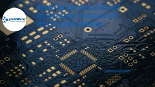
The semiconductor industry, with its rapid technological progression and intricate manufacturing processes, relies heavily on precision and control for optimum yield. In this sphere, an element that has become crucial to maintaining high-quality standards is advanced wafer mapping. By harnessing state-of-the-art algorithms, distinctive color-coded grids, and innovative software features, wafer mapping software furnishes a high-resolution analysis of semiconductor wafers in real time. This capability, in turn, boosts the efficacy and output of the semiconductor manufacturing industry. The ensuing discussion elucidates the fundamentals and advancements in wafer mapping, spotlighting its crucial role in semiconductor production.

Recommended
Recommended
More Related Content
Similar to Amplifying the Power of Efficient Semiconductor Production with Next-Gen Wafer Mapping.pptx
Similar to Amplifying the Power of Efficient Semiconductor Production with Next-Gen Wafer Mapping.pptx (20)
More from yieldWerx Semiconductor
More from yieldWerx Semiconductor (13)
Recently uploaded
Recently uploaded (20)
Amplifying the Power of Efficient Semiconductor Production with Next-Gen Wafer Mapping.pptx
- 1. Amplifying the Power of Efficient Semiconductor Production with Next-Gen Wafer Mapping https://yieldwerx.com/
- 2. The semiconductor industry, with its rapid technological progression and intricate manufacturing processes, relies heavily on precision and control for optimum yield. In this sphere, an element that has become crucial to maintaining high-quality standards is advanced wafer mapping. By harnessing state-of-the-art algorithms, distinctive color-coded grids, and innovative software features, wafer mapping software furnishes a high-resolution analysis of semiconductor wafers in real time. This capability, in turn, boosts the efficacy and output of the semiconductor manufacturing industry. The ensuing discussion elucidates the fundamentals and advancements in wafer mapping, spotlighting its crucial role in semiconductor production. Decoding the Vital Role of Wafer Mapping in Semiconductor Manufacturing The lifecycle of a silicon wafer, transitioning from its crystalline form to the final semiconductor device, comprises a series of accurately planned and supervised fabrication steps. Among these, Wafer Mapping holds immense significance. Devised initially in the 1970s to oversee ion implantation uniformity, wafer mapping has now become an integral component in the landscape of modern semiconductor manufacturing. It discloses intricate aspects of the performance of a semiconductor device and helps identify irregularities that could potentially impact the yield. Demystifying the Color-Coded Grid: The Backbone of Wafer Mapping The principle of wafer mapping banks on a color-coded grid that portrays device performance on the substrate surface. This grid illustration constitutes a fundamental aspect of the "wafer map." The mapping process is facilitated by software frequently referred to as the "wafer map generator". It acts as the die per wafer calculator, where each color represents a unique quality or performance parameter of the die. This color coordination allows for easy visualization of the operational and non-operational dies, thereby contributing to detailed analysis and comprehension of the wafer yield.
- 3. Cutting-Edge Features and Functionalities in Wafer Mapping Software Contemporary wafer mapping software brings forth advanced features such as die grading, merging wafers on the map, hard and soft bins dissection, and other operational functions. Each of these features is meticulously designed to enhance the yield and quality of the semiconductor wafer. Die grading classifies dies based on product quality and reliability. Merging wafers enables a comprehensive analysis of multiple wafers at once. Hard and soft bin dissection differentiates between permanent and temporary failures, thus offering a holistic view of the wafer's health. Tackling Challenges in Wafer Yield Calculation Historically, wafer yield calculation posed a significant challenge due to the complex requirements of data collection, the need for specialized knowledge, and the intricate nature of the semiconductor process. However, modern yield management solutions now offer real-time wafer mapping capabilities, thus reducing these challenges. These systems are capable of collecting, loading, reading, and generating wafer maps from semiconductor test data, offering immediate insights into wafer health and quality concerns. Wafer Acceptance Test (WAT): A Crucial Pre-requisite Before Fabrication Before the fabrication process, each wafer undergoes a comprehensive testing procedure known as the Wafer Acceptance Test (WAT). The results are collated and visualized using a JMP wafer map. This map discloses spatial information on faulty integrated circuits on a silicon wafer, providing vital data for statistical analysis to monitor process quality. By identifying and classifying defect patterns on the wafer map, manufacturers can pinpoint failures in the manufacturing process and implement necessary modifications to improve wafer production yield.
- 4. Navigating Complex Defect Patterns in Modern Semiconductor Manufacturing Despite these advancements, there remain challenges to be surmounted. As semiconductor manufacturing technology has advanced, defect patterns have become increasingly complex. Defects can vary in shape, size, and location, making their accurate recognition and classification a formidable task. The task is further complicated by the unequal number of different defect patterns on the wafer map and the similarities in defect shape and position information, which often makes the identification of certain classes challenging. Leveraging Excel Wafer Map for Superior Defect Analysis To address these challenges, advanced analysis methods and tools such as Excel Wafer Map can be employed. The Excel Wafer Map is a readily accessible and user-friendly tool for wafer data analysis. It is compatible with various wafer map formats and can convert these maps into an Excel sheet. Users can then manipulate this data, utilizing Excel's built-in statistical analysis and data visualization features to gain a better understanding of the defects and yield. The Significance of a "Die Per Wafer Calculator" in Yield Optimization The development and continuous refinement of wafer map software have substantially contributed to the semiconductor manufacturing industry's ability to maintain high-quality standards and optimize yields. A key element of this process is the use of a "die per wafer calculator." This tool assists in determining the maximum number of good dies that can be produced from a wafer, a factor that directly impacts the profitability of the semiconductor manufacturing process. The accuracy and ease of using a die per wafer calculator, especially when it is integrated into wafer mapping software, can enable real-time analysis and informed decision-making in manufacturing scenarios.
- 5. The Cruciality of Wafer Lot Consistency in Manufacturing Another critical aspect of wafer mapping is the importance of the wafer lot in semiconductor manufacturing. A wafer lot comprises a group of wafers that are processed together through the various stages of semiconductor production. Consistency within a wafer lot is critical, as inconsistencies can lead to variations in the final product, ultimately affecting the yield. The wafer mapping software aids in identifying such variations within the lot, thereby maintaining the lot's integrity and enhancing the overall yield. The Indispensable Role of Wafer Maps in Testing Process Moreover, wafer testing is an indispensable process in semiconductor manufacturing, ensuring the quality of the wafers before they are moved into the assembly line. At this stage, wafer maps serve as a critical tool. They facilitate a visual understanding of the state of each wafer, contributing to an efficient testing process. For instance, a wafer map can illustrate areas with high defect density, enabling targeted testing efforts and conservation of resources. The Art of Calculating Wafer Yield: The Final Step in Manufacturing The manufacturing process of a wafer culminates with the wafer yield, which refers to the number of good, functioning dies that can be derived from a wafer. Calculating this yield necessitates an understanding of the initial number of dies on the wafer and the number of dies that have failed the testing process. In this regard, a wafer yield formula comes into play, calculating the final yield based on these parameters. The wafer map, in conjunction with the yield formula, can provide an accurate yield calculation, thereby offering insights into the effectiveness of the manufacturing process.
- 6. Integrated Tools for Seamless Semiconductor Manufacturing By integrating the capabilities of the die per wafer calculator, wafer lot analysis, wafer testing, and the wafer yield formula within the wafer mapping software, semiconductor manufacturing can be transformed into a highly streamlined and efficient process. These integrated tools can aid in identifying potential areas of concern at an early stage, offer detailed insights into the manufacturing process, and pave the way for timely interventions, leading to improved yield and productivity. Conclusion To conclude, wafer mapping holds a cardinal role in semiconductor manufacturing. It assists in streamlining the manufacturing process by identifying and categorizing defects, thus enabling improvement in wafer yield. While it does present challenges, the continuous evolution of wafer mapping software and tools assures the industry of As semiconductor devices continue to evolve, so too will the tools and methodologies used to manufacture them. References: 1. W. Maly, "Computer Analysis of Wafer Maps," IEEE Transactions on Semiconductor Manufacturing, vol. 4, no. 4, pp. 374-378, Nov. 1991. 2. N. Semiconductors, "The Importance of Wafer Mapping in Semiconductor Manufacturing," Nanometrics Blog, 29 Oct. 2018. 3. "Wafer mapping - The key to high yield in semiconductor manufacturing," VLSI Research Europe, 2 April 2016. 4. M. Sekanina, "Evolvable hardware solution for real-time image filtering," Proceedings of the 2002 NASA/DOD Conference on Evolvable Hardware, pp. 123-130, July 2002. 5. Y. Huang, P. Gu, "Computer-aided process planning: The state-of-the-art survey," International Journal of Production Research, vol. 28, no. 4, pp. 739-760, 1990.