1. Advance Physics Letter
________________________________________________________________________________
_______________________________________________________________________________________
ISSN (Print) : 2349-1094, ISSN (Online) : 2349-1108, Vol_1, Issue_1, 2014
26
Organic Light Emitting Diode: “A New Era in Display Techniques”
Raounak Kumar Pandey, Srikant Kumar, Prashant Kumar, Amit Kumar, Gajendra Singh Rathore*
,
Chitrakant Sharma
Department of Electronics and Communication Engineering, School of Engineering & IT,
MATS University, Gullu, Aarang, Raipur, C.G., INDIA
Email : raounakpandey121@gmail.com, gajendra05in@gmail.com*
Abstract -This article is a study of various parameters of
Organic Semiconductor light emitting device such as
transmittance, reflectance, thickness, absorption, refractive
index, extinction coefficient, life time and out coupling
efficiency. We are fabricating an organic display device
using Thin Film Spray Pyrolysis Deposition Method. ITO
glass substrate, Alq3 we are using for providing potential
gradient to emissive layer.
Organic Light Emitting Diodes (OLED), a quantum leap in
display technology in the field of organic display was
achieved in 1987 by Tang and Van Slyke from Kodak where
they developed an efficient OLED by using p-n
heterostructure devices including thin film and organic
material. Inside the OLED emissive electroluminescent layer
is fully organic film and it emits light when current applied
on it. Organic Light Emitting Diode devices are new rising
technology with high convenience in display market. On the
other hand, is a portable, reusable display medium, typically
thin and flexible. An enormous amount of research effort
into the field all around the globe has made it sufficient to
compete with other display technology rather now it is ahead
of any available display technique.
Keywords: OLED, ITO, Alq3, Transmittance, Absorbance,
Extinction Co-efficient, Spray Pyrolysis.
I. INTRODUCTION
The basic organic devices are formed in sheets where a
layer located in between cathode and anode known as
emissive organic layer and substrate deposited on it. The
OLED substrate can be glass or metal or a polymer
plastic. Organic light-emitting devices operate on the
phenomenon known as electroluminescence in which
the electrical energy is converted into light.
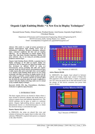
Passive Matrix OLED
In PMOLED’s the strips are placed like rows and
columns in between the organic layer in other side of the
substrate. PMOLED’s required more power as compared
to the other OLED’s.
Fig 1. Structure of AMOLED
Active Matrix OLED
In AMOLED’s the organic layer placed in between
cathode and anode. Anode layer consist of black thin
film transistor (TFT) which forms a matrix. It possess
two TFT array per pixels one to start and second to stop
the charge, so this device consumes less power than
passive devices.
Fig 2. Structure of PMOLED
2. Advance Physics Letter
________________________________________________________________________________
_______________________________________________________________________________________
ISSN (Print) : 2349-1094, ISSN (Online) : 2349-1108, Vol_1, Issue_1, 2014
27
WORKING
Fig 3. Working of OLED
OLED’s are made using thin films of organic material
which are sandwiched in between an anode and cathode.
There are a variety of organic materials that can be used
for such films. The general structure for an OLED
consists of four thin film layers deposited on a substrate.
The first layer is the cathode which is typically made of
Mg:Ag. Under this layer is an electron transport layer,
typically made of Alq3. The third layer is the hole
transport layer. Lastly, fourth layer is the anode, which
is typically made of indium-tin-oxide (ITO). The
substrate is made of either a glass or transparent plastic.
When a voltage is applied across the two inner layers the
holes and electrons combine forming excitons. When an
exciton decays, a photon is emitted [4].
Layer Thickness
Fig 4.Thickness of OLED Layers
II. MATERIALS FOR FABRICATION
ITO (Indium tin oxide) is widely used in transparent
display technology .It have two major property first is
Electrical conductivity and second is Optical
transparency so we use ITO as an anode in our project.
As we increase it thickness the conductivity decreases
and vice versa.
Hole Transporting layer- N, N’-bis (naphthalen-1-yl)-
N,N'-bis (phenyl) benzidine.
Electron Transporting Layer / Emission
Transporting Layer : Since the first report of efficient
and stable OLEDs [1,2], tris (8- hydroxyquinoline)
aluminum (Alq3) –which is used as the emission and
electron transport layer, the interest in this archetype
material is persistent. Properties such as relative
stability, easy synthesis, good electron transport, and
emitting properties result in extensive application of
Alq3 in OLED design. Tang and coworkers discovered
Alq3-based multi-layer thin-film electroluminescent
devices in 1987[1]. Alq3 still continues to be the
workhorse among the class of low molecular weight
materials for OLEDs. Research into organic materials
for use in OLEDs has mostly focused on conjugated
polymers or low molecular weight materials [3].
Cathode- Aluminum is remarkable for the metal's
low density. Aluminum is a relatively soft, durable,
lightweight, ductile and malleable metal with
appearance ranging from silvery to dull gray, depending
on the surface roughness. Aluminum is a
good thermal and electrical conductor, having 59% the
conductivity of copper, both thermal and electrical,
while having only 30% of copper's density.
III. SPRAY PYROLYSIS METHOD
Technique we considered for deposition of thin film
layers of OLED. Unlike many other film deposition
techniques, spray pyrolysis represents a very simple and
relatively cost-effective processing method (especially
with regard to equipment costs). It offers an extremely
easy technique for preparing films of any composition.
Spray pyrolysis does not require high-quality substrates
or chemicals. The method has been employed for the
deposition of dense films, porous films, and for powder
production. Even multilayered films can be easily
prepared using this versatile technique [5].
3. Advance Physics Letter
________________________________________________________________________________
_______________________________________________________________________________________
ISSN (Print) : 2349-1094, ISSN (Online) : 2349-1108, Vol_1, Issue_1, 2014
28
Fig 5. Thin Film Deposition Technique
IV. EFFECTIVE PARAMETERS
Transmittance & Absorption
Some compounds absorb light and some does not absorb
the light. According to the spectroscopy the
transmittance is the incident light passing through the
sample.
In the above figure Light (Po) entering the sample and
absorption takes place and it comes out in after leaving
the sample its value is (P).
According to Beer’s Law,
Transmittance – T = P/Po
Absorption – A = log10 Po/P
Thickness
(cm)
0 0.2 0.4 0.6 1.0
%T 100 50 25 12.5 3.125
Absorbance 0 0.3 0.6 0.9 1.5
0.0 0.2 0.4 0.6 0.8 1.0
0
20
40
60
80
100
%Transmittance(%)
Thickness (cm)
% Transmittance
Absorbance
Fig 5. Plot Thickness v/s Transmittance & Absorbance
Extinction Coefficient
We are using Ellipsometry method for calculating the
complex refractive index of thin film formed over the
substrate. A measure of the rate of diminution of
transmitted light via scattering and absorption for a
medium. It is a parameter defining how strongly a
substance absorbs light at a given wavelength as per
mass density or per molar concentration.
Thickness
Again Ellipsometry method we are using for calculating
the thickness of film. Typically, the measured signal is
the change in polarization as the incident radiation (in a
known state) interacts with the material structure of
interest (reflected, absorbed, scattered, or transmitted).
The polarization change is quantified by the amplitude
ratio, Ψ, and the phase difference, Δ. Because the signal
depends on the thickness as well as the materials
properties. Ellipsometry can be a universal tool for
contact free determination of thickness and optical
constants of films of all kinds.
V. CONCLUSION
An entirely new era in display technology that offers
improved performance as well as novel applications, is
molded with the application of organic semiconductor
for display application. Full color displays using OLEDs
are in the position to replace LCDs in the small scale
display market. OLEDs offer a decreased manufacturing
cost, a brighter, more vibrant display, as well as a larger
viewing angle. Lower power consumption makes OLED
perfect for portable devices which rely on battery power.
Current research all around the globe is focused in
increasing its brightness, lifetime and out coupling
efficiency.
VI. ACKNOWLEDGEMENT
We are grateful to Mr. M.K.Pradhan Sir, Head,
Department of Electronics and Communication
Engineering, for his motivational thoughts and constant
support. We would also like to thanks all the faculties of
4. Advance Physics Letter
________________________________________________________________________________
_______________________________________________________________________________________
ISSN (Print) : 2349-1094, ISSN (Online) : 2349-1108, Vol_1, Issue_1, 2014
29
Electronics and Communication Engineering
Department for their encouragement.
REFERENCE
[1] C. Tang and S.VanSlyke, Appl. Phys. Lett. 51,
913 (1987).
[2] Stefan Berleb and Wolfgang Brutting Phys Rev
Lett.89, 286601 (2002).
[3] John E. Knox, Mathew D. Halls, Hrant P.
Hratchian and H. Bernhard Schle.
[4] Chris Summitt, “OLED Fabrication for Use in
Display Systems”, (2006).
[5] Gajendra Singh Rathore, Chitrakant Sharma,
“Thin Film Fabrication Using Spray Pyrolysis
Technique”, International Journal of Research in
Advent Technology, 50-54 (2014).
[6] Blanchet, G. and Rogers, J.A., “Printing
techniques for plastic electronics”. J. Inf. Sci.
Technol., 47, 296–303 (2003).
[7] H. Kawaguchi, T. Someya, T. Sekitani, and T.
Sakurai, “IEEE Journal of Solid-State Circuits”,
40, 177 (2005).
[8] L. S. Hung, C. H. Chen, “Materials Science and
Engineering”, (2006)

![Advance Physics Letter
________________________________________________________________________________
_______________________________________________________________________________________
ISSN (Print) : 2349-1094, ISSN (Online) : 2349-1108, Vol_1, Issue_1, 2014
27
WORKING
Fig 3. Working of OLED
OLED’s are made using thin films of organic material
which are sandwiched in between an anode and cathode.
There are a variety of organic materials that can be used
for such films. The general structure for an OLED
consists of four thin film layers deposited on a substrate.
The first layer is the cathode which is typically made of
Mg:Ag. Under this layer is an electron transport layer,
typically made of Alq3. The third layer is the hole
transport layer. Lastly, fourth layer is the anode, which
is typically made of indium-tin-oxide (ITO). The
substrate is made of either a glass or transparent plastic.
When a voltage is applied across the two inner layers the
holes and electrons combine forming excitons. When an
exciton decays, a photon is emitted [4].
Layer Thickness
Fig 4.Thickness of OLED Layers
II. MATERIALS FOR FABRICATION
ITO (Indium tin oxide) is widely used in transparent
display technology .It have two major property first is
Electrical conductivity and second is Optical
transparency so we use ITO as an anode in our project.
As we increase it thickness the conductivity decreases
and vice versa.
Hole Transporting layer- N, N’-bis (naphthalen-1-yl)-
N,N'-bis (phenyl) benzidine.
Electron Transporting Layer / Emission
Transporting Layer : Since the first report of efficient
and stable OLEDs [1,2], tris (8- hydroxyquinoline)
aluminum (Alq3) –which is used as the emission and
electron transport layer, the interest in this archetype
material is persistent. Properties such as relative
stability, easy synthesis, good electron transport, and
emitting properties result in extensive application of
Alq3 in OLED design. Tang and coworkers discovered
Alq3-based multi-layer thin-film electroluminescent
devices in 1987[1]. Alq3 still continues to be the
workhorse among the class of low molecular weight
materials for OLEDs. Research into organic materials
for use in OLEDs has mostly focused on conjugated
polymers or low molecular weight materials [3].
Cathode- Aluminum is remarkable for the metal's
low density. Aluminum is a relatively soft, durable,
lightweight, ductile and malleable metal with
appearance ranging from silvery to dull gray, depending
on the surface roughness. Aluminum is a
good thermal and electrical conductor, having 59% the
conductivity of copper, both thermal and electrical,
while having only 30% of copper's density.
III. SPRAY PYROLYSIS METHOD
Technique we considered for deposition of thin film
layers of OLED. Unlike many other film deposition
techniques, spray pyrolysis represents a very simple and
relatively cost-effective processing method (especially
with regard to equipment costs). It offers an extremely
easy technique for preparing films of any composition.
Spray pyrolysis does not require high-quality substrates
or chemicals. The method has been employed for the
deposition of dense films, porous films, and for powder
production. Even multilayered films can be easily
prepared using this versatile technique [5].](data:image/gif;base64,R0lGODlhAQABAIAAAAAAAP///yH5BAEAAAAALAAAAAABAAEAAAIBRAA7)