Commercializing Nanomaterials Bridging The Gap Shankar
•
1 like•632 views

Challenges & Opportunities in commercializing Nanomaterials Presented in National Conference on Nanomaterials, Feb 2009

Recommended
Recommended
More Related Content
Viewers also liked
Viewers also liked (18)
Similar to Commercializing Nanomaterials Bridging The Gap Shankar
Similar to Commercializing Nanomaterials Bridging The Gap Shankar (20)
Commercializing Nanomaterials Bridging The Gap Shankar
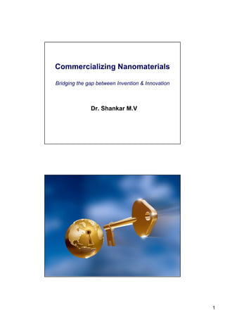
- 1. Commercializing Nanomaterials Bridging the gap between Invention & Innovation Dr. Shankar M.V Feb 09 Commercializing Nanomaterials - Bridging the gap 2 1
- 2. Feb 09 Commercializing Nanomaterials - Bridging the gap 3 Thus, the task is, not so much to see what no one has yet seen; but to think what nobody has yet thought, about that which everybody sees. Erwin Schrodinger Feb 09 Commercializing Nanomaterials - Bridging the gap 4 2
- 3. Innovation is bringing an insightful idea successfully to the Market Jan ver loop (Shell) Feb 09 Commercializing Nanomaterials - Bridging the gap 5 Creativity & Ideas are not enough, they need to be structured, defined and directed to result in Innovation Feb 09 Commercializing Nanomaterials - Bridging the gap 6 3
- 4. It doesn’t matter where scientific discoveries and breakthrough technologies originate – for national prosperity, the important thing is who commercializes them. McKinsey Quarterly, Amar Bhide. Feb 09 Commercializing Nanomaterials - Bridging the gap 7 Top 3 Barriers to Commercialization • Technology Barriers • Acceptance Barriers • Intellectual Property Barriers Feb 09 Commercializing Nanomaterials - Bridging the gap 8 4
- 5. Need for Product-focus Industry funds Revenue from Nanomaterials Breakthrough NPS Research Discovery New Materials Happy Processes Customer Applications New Products Development Better Performance Feb 09 Commercializing Nanomaterials - Bridging the gap 9 Technology Barriers to Commercialization • (1) Product Focus • (2) Affordable Cost • (3) Speed Feb 09 Commercializing Nanomaterials - Bridging the gap 10 5
- 6. Nano R&D – Old Paradigm Discovery- based Science & Product Development 70 % Effort 20 % 10 % Discover Determine Novel Nanomaterial Identify Assess Nanostructures & properties Potential Commercial Nanomaterials Processing- Viability Applications through Structure- exploratory Property research Correlations Feb 09 Commercializing Nanomaterials - Bridging the gap 11 Nanomaterials enter limited Markets Nano R&D – New Paradigm Application - based Problem-solving 50 % Effort 50 % Identify existing Design unfulfilled Needs Nanomaterials Tune properties & Determine customize Nanomaterial with required production Problems properties Properties to meet required to meet diverse product the Need requirements & Challenges in Scale-up Markets end-uses Synthesis Feb 09 Commercializing Nanomaterials - Bridging the gap Nanomaterials enter New Markets 12 6
- 7. Acceptance Barrier to Commercialization • Safe production • Safe use • Safe disposal Feb 09 Commercializing Nanomaterials - Bridging the gap 13 Feb 09 Commercializing Nanomaterials - Bridging the gap 14 7
- 8. Feb 09 Commercializing Nanomaterials - Bridging the gap 15 IP Barrier to Commercialization • Securing IP • Freedom to Practise • Monetising IP Feb 09 Commercializing Nanomaterials - Bridging the gap 16 8
- 9. Nanotech Patents • Original IBM patent on STM – 4343993 – 1986 Nobel Prize in Physics • Nano Imprint Lithography – Stephen Chou – Chad Mirkin – Dip Pen Nano Lithography – 6827979 – Startup NanoInk • Carbon Nanotubes – NEC – Ijima – 5747161 (Sept 1992) – IBM, 1993 • Quantum Dots – Paul Alivisatos (Berkeley) 5505928, Moungi Bawendi (MIT) 6322901 • Organic LED – 5247190 – Richard Friend – Conjugated Polymers that glow – Cambridge Display Technologies Feb 09 Commercializing Nanomaterials - Bridging the gap 17 Nanomaterials-based Products some recent examples…. Feb 09 Commercializing Nanomaterials - Bridging the gap 18 9
- 10. Catalysts Optoelectronic Devices Carbon black in Tires Sunscreens Nano CMP Slurries Semiconductor processing Plasma Spray ed iz Nanocoatings al ials ci er er m at les m om p Co an xam N E Discovery of a Black Hole & the nano connection • Astronomers discover the largest black hole ever found. 3.5 billion light years away, around 18 billion times heavier than our sun. • 150 worked for ~ 9 years before the heart piece for Germany’s first large telescope was finished: record-breaking mirror substrate diameter 3.6 m, 60 cm thick. • Excellent material characteristics – isotropic, homogeneous and can be polished rather easily – mainly leverages its strengths in areas where the highest possible precision is important, optics – dimensional specs a few thousandths of micrometers. • 40 years ago, a new material was born: a glass ceramic Zerodur®. SCHOTT succeeded in producing a material with a coefficient of expansion close to zero • The secret lies in the well-balanced mixture of crystallites 30 to 50 nm in size embedded inside a glass matrix of lithium, aluminum and silicon oxides. Source - SCHOTT Feb 09 Commercializing Nanomaterials - Bridging the gap 20 10
- 11. Discovery of a Black Hole & the nano connection • The new ZERODUR® K20 glass ceramic material contains a crystal phase of over 90% Keatite, produced by thermal transformation from the semi-transparent ZERODUR® glass ceramic material. • This new material has an expansion coefficient of 2.0•10-6 K-1 between 20°- 700°C, and an even lower value of 1.5•10-6 K-1 at room temperature. The material has high Source - SCHOTT temperature stability and does not change during multiple temperature cycles. After transformation the material has a radiance factor of more than 90% with a • Advantages of ZERODUR® K20 glass ceramic matt brilliant white finish. include: Optical inspection of the excellent ZERODUR® K20 is free of pores and homogeneity and internal quality can be done can be polished to very low surface in the semi transparent base material before transformation. roughness levels. Large-scale parts can be produced with dimensions of several meters. Feb 09 Commercializing Nanomaterials - Bridging the gap 21 Hydrophobic surfaces Nano to mimik the lotus leaf Source: http://www.nanoshop.com/ Feb 09 Commercializing Nanomaterials - Bridging the gap 22 11
- 12. Hydrophobic surfaces Nano to mimik the lotus leaf • Hydrophobic coating such as Diamon- Fusion®, applied on car windshields and side glass, improves visibility during rainy conditions over 30%, improving response time by 25%, which translates into an invaluable safety feature. • NEW Diamon-Fusion® spray/wipe-on coating method of applying the patented Diamon- Fusion® makes field applications more effective (especially quicker and easier to apply) and with far less equipment and therefore equipment maintenance and the quality is on a par with the DFI vapor method. • This NEW method of application of DFI’s nanotechnology also creates a cross-linked and branched, capped silicone film, and the bond is still a covalent bond (sharing electrons with the glass itself). Like DFI’s vapor method, but non-chlorinated, the chain of atoms manipulated during this chemical process is also done at nano-scale levels. http://www.diamondfusion.com.au/ Feb 09 Commercializing Nanomaterials - Bridging the gap 23 Hydrophobic surfaces Nano to mimick the lotus leaf • DFI’s nanotechnology, Diamon-Fusion®, uses a chemical vapor deposition process. DFI’s nanotechnology is DFI’s NANO-CHEMISTRY applicable to most surfaces containing silica (silicon dioxide) such as glass, ceramic tile, porcelain, and granite. The The chemical reaction bonds to form an ultra-thin protective specially formulated vapors react with the moisture on the layer of optically clear durable material, a nanostructurated surface and the silica in the substrate (to be treated). DFI’s device, making the surface significantly easier to clean and nanotechnology is generated by a two-stage chemical more resistant to weathering. This method is done at nano- process: scale levels, thus also called ‘nano-chemistry’, which is a length scale of approximately 1 – 100 nanometer range (1 • Stage 1 nanometer is 1/1,000,000,000 meter, or 1 billionth of a meter). Nanometer dimensions are at the atomic dimension scale. The chemical reaction created in the first stage causes a “cross-linked” and “branched” silicone film to be grown from DFI’s COVALENT BOND below the surface out. After converting the chlorine atoms to OH groups using additional moisture (chlorine was left at the end of the atom chains after the first stage), a second The bond created in the patented process is a covalent specially formulated vapor is introduced to the surface. bond, the strongest possible bond, in chemical terms that a hydrophobic coating can generate. A covalent bond means that the coating shares the electrons within the glass itself, • Stage 2 thus becoming a part of the glass. Covalent Bonds are approximately 10 times stronger than hydrogen-bridge The second stage ‘caps’ the entire chain of atoms. This bonds, which are commonly present in most other water unique ‘capping’ substantially increases the hydrophobicity repellent coatings. and durability, leaving, chemically speaking, no points of attachment for contaminants and creating a truly repellant charge. Feb 09 Commercializing Nanomaterials - Bridging the gap 24 12
- 13. What do you need to Innovate Creative Expertise Thinking Motivation 25 Elements of Innovation Motivation Choose a problem Creativity Define Brainstorm the problem ideas Select Validate Implement Expertise ideas ideas ideas 26 13
- 14. What’s Possible Vs What’s Needed ? Practicality - What’s needed ? Einstein: Business-driven Pasteur: Imagination is more important than knowledge. Knowledge Low Need High Need In the field of observation, is limited. Imagination chance favors only encircles the world. the prepared mind High Quest Edison: Curiosity I never perfected an invention that I did What’s Possible ? not think about in Science-driven terms of the service it might give others... I find out what the world needs, then I proceed to invent.... Low Quest Pasteur’s quadrant – Strategic Research 27 Edison - Inventor of the Electric Bulb Innovator of Electric Illumination Creative Strong analytical power Entrepreneurship The drive to succeed I find out what the World needs and then proceed to invent it 1% Inspiration, 99% Perspiration 28 14
- 15. Inventor, Innovator & Entrepreneur Discovery - 1802 – Humphrey Davy discovered that an electric current passing through metal wire could give light. Formulation of the Problem - 1878 – Edison, “ the electric light idea took possession of me It was easy to see what the thing needed It wanted to be subdivided The light was too bright and too big. What we wished for was little lights and a distribution of them in people’s houses in a manner simillar to gas.”. Patent – 1879 – demonstrated 40 h lifetime Started Edison Electric Light Company Key Idea – Only If electricity is distributed similar to gas, could the electric bulb become economically attractive. 29 Inventor, Innovator & Entrepreneur 1880 – Edison improved Bulb’s life to 300h, developed a dynamo to generate electricity at 110V, small distribution net, Demo with 425 lamps at Menlo Park. 30 15
- 16. Inventor, Innovator & Entrepreneur Edison becqme an entrepreneur & started three new companies to manufacture the equipment. 1892 - Edison Electric Illuminating Company Lighted up Wall Street in New York. 31 Inventor, Innovator & Entrepreneur Edison brought a significant invention, based on breakthrough technology and requiring a new infrastructure, successfully to Market. Key Idea – Divide a big problem into a series of small ones and solve them while keeping whole value chain in mind. 32 16
- 17. Top 3 Barriers to Commercialization • Technology Barriers • Acceptance Barriers • Intellectual Property Barriers Feb 09 Commercializing Nanomaterials - Bridging the gap 33 17