
Recommended
More Related Content
What's hot
What's hot (20)
Similar to 1 reliability qualification report pcb
Similar to 1 reliability qualification report pcb (20)
Recently uploaded
Recently uploaded (20)
1 reliability qualification report pcb
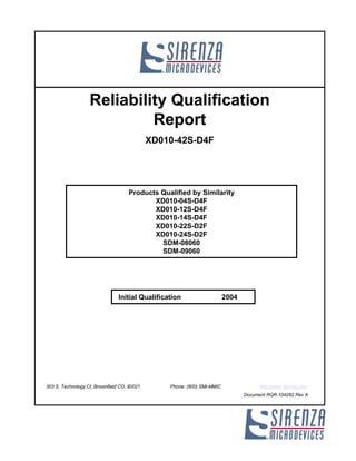
- 1. Reliability Qualification Report XD010-42S-D4F Products Qualified by Similarity XD010-04S-D4F XD010-12S-D4F XD010-14S-D4F XD010-22S-D2F XD010-24S-D2F SDM-08060 SDM-09060 Initial Qualification 2004 303 S. Technology Ct, Broomfield CO, 80021 Phone: (800) SMI-MMIC http://www.sirenza.com Document RQR-104282 Rev A
- 2. XD010-42S-D4F Reliability Qualification Report I. Qualification Overview The XD010-42S-D4F has demonstrated reliable operation by passing all qualification testing in our product qualification test plan. It has been subjected to stresses such as High Temperature Operational Life, High Temperature Storage, Temperature Cycling, as well as Mechanical Shock and Vibration. II. Introduction The XD010-42S-D4F 10W power module is a 2-stage Class A amplifier designed for use in the driver stages of linear RF power amplifiers for cellular base stations. It operates from a single voltage and has internal temperature compensation. III. Fabrication Technology This amplifier is manufactured using XeMOS® II, a 0.8µm, metal source contact, aluminum metallization process which utilizes a discrete Laterally Diffused MOSFET (LDMOS) transistor to achieve RF performance capabilities for the wireless communications and networking markets. The XeMOS® II process embodies the conventional NMOS processing techniques with additional features enabling it capable of high voltage, high power and high frequency operation at power levels of up to 60W at frequencies up to 2.5 GHz. IV. Package Type The XD010-42S-D4F is a hybrid chip and wire assembly. The printed circuit board is connected to a tin/copper base plate with a eutectic solder attach. The lid is attached to the PCB with a B stage epoxy. Figure 1 : Photograph of XD010-42S-D4F
- 3. XD010-42S-D4F Reliability Qualification Report V. Qualification Methodology The Sirenza Microdevices qualification process consists of a series of tests designed to stress various potential failure mechanisms. This testing is performed to ensure that Sirenza Microdevices products are robust against potential failure modes that could arise from the various die and package failure mechanisms stressed. The qualification testing is based on JESD test methods common to the semiconductor industry. The manufacturing test specifications are used as the PASS/FAIL criteria for initial and final tests. Qualification tests are performed on the wafer fabrication process to demonstrate semiconductor reliability. In addition, package testing is also performed. These qualification results are detailed in Section XII. VI. Qualification By Similarity A device can be qualified by similarity to previously qualified products provided that no new potential failure modes/mechanisms are possible in the new design. The following products are qualified by similarity: XD010-04S-D4F XD010-12S-D4F XD010-14S-D4F XD010-22S-D2F XD010-24S-D2F SDM-08060 SDM-09060 VII. Operational Life Testing Sirenza Microdevices defines operational life testing as a DC biased elevated tempera- ture test performed at or near the maximum channel temperature limit. The purpose of the operational life test is to statistically show that the product operated at its maximum operational ratings will be reliable. The results for this test are expressed in device hours that are calculated by multiplying the total number of devices passing the test by the number of hours tested. HTOL Completion Test Channel Quantity Device Hours Date Duration Temperature August 2004 1000 175°C 15 15,000 hours
- 4. XD010-42S-D4F Reliability Qualification Report IX. Electrostatic Discharge Classification Sirenza Microdevices classifies Human Body Model (HBM) electrostatic discharge (ESD) according to the JESD22-A114 convention. All pin pair combinations were tested. Each pin pair is stressed at one state voltage level using 1 positive and 1 negative pulse polarity to determine the weakest pin pair combination. The weakest pin pair is tested with 3 devices below and above the failure voltage level to classify the part. The Pass Fail status of a part is determined by the manufacturing test specification. The ESD class quoted indicated that the device passed expose to certain voltage, but does not pass the next higher level. The following table indicates the ESD sensitivity classification levels. The XD010-42S-D4F is a class 3B device. Class Passes Fails Device Class 0 0V <250 V XD010-42S-D4F 3B 1A 250 V 500 V All others 3B 1B 500 V 1000 V 1C 1000 V 2000 V 2 2000 V 4000 V 3A 4000 V 8000 V 3B 8000V X. Qualification Test Results for XD010-42S-D4F Group A1 Temperature Cycling Loose Device (Air to Air Thermal Shock) Test Conditions Temperature Range -55°C to 125°C, 10 min dwell, 1 minute transition, 200 cycles Number of 9 Test JESD22-A104 Results PASS Devices Under Standard Test Group A2 High Temperature Operational Life Test Conditions Channel Temperature = 175°C, Test Duration = 1000 hours Number of 15 Test JESD22-A108 Results PASS Devices Under Standard Test
- 5. XD010-42S-D4F Reliability Qualification Report X. Qualification Test Results for XD010-42S-D4F (con’t) Group D High Temp Storage Test Conditions Temperature = 100°C, Test Duration = 1000 hours Number of 10 Test JESD22-A103 Results PASS Devices Under Standard Test Group H Solderability Test Conditions Dip & Look; Steam Age Condition C, 8hrs; Solder Dip Condition A, 215C Number of 10 Test JESD22-B102 Results PASS Devices Under Standard Test Group E Vibration + Mechanical Shock Number of 5 Test JESD22-B103 Results PASS Devices Under Standard JESD22-B104 Test
- 6. XD010-42S-D4F Reliability Qualification Report XI. Junction Temperature Determination One key issue in performing the qualification testing is to accurately determine the junction temperature of the device. Sirenza Microdevices uses a 3um spot size infrared camera that allows a device to be measured at its normal operational parameters. The 3um spot size allows for very good resolution compared to the heated area of the transistor, which in this case is approximately 1-2um. The results for the 1st stage, running at maximum operational current of 230mA, a device voltage of 28V, and a base plate lead temperature of 90oC are as follows: Figure 2: Infrared Thermal Image of Stage 1, XD010-42S-D4F
- 7. XD010-42S-D4F Reliability Qualification Report XI. Junction Temperature Determination (con’t) The results for the 2nd stage, running at maximum operational current of 1001 mA, a device voltage of 28V, and a base plate lead temperature of 90 oC are as follows: Figure 3: Infrared Thermal Image of Stage 2, XD010-42S-D4F
- 8. XD010-42S-D4F Reliability Qualification Report XII. XeMOS® II Process Qualification The XeMOS® II process qualification test vehicle uses a 30W die packaged in a ceramic A191 package using a Au/Si eutectic die attach and wire bonded with aluminum wire. The cumulative qualification results are summarized in the table below. (Reference RQR-104230) Test Description Test Standard/Method Lot # (s) Qty Qty Results* In Out High Temperature MIL-STD-750 394063 18 18 Pass Gate Bias (HTGB) Method 1042.3 3A4555 16 16 Pass Test Cond. B 372665 16 16 Pass Gate Bias = 16V Temp = 175C, Time = 48hrs High Temperature MIL-STD-750 3A4555 16 16 Pass Reverse Bias Method 1042.3 372665 16 16 Pass (HTRB) Test Cond A, M394063 16 16 Pass Bias Volt. = 48V Temp = 175C Time = 160hrs Temperature JESD22-A110B M394063 13 13 Pass Humidity, Unbiased paragraph 3.1, row 1 351106 16 16 Pass 500 Hours 372665 19 19 Pass Temperature JESD22-A110B 372665 13 13 Pass Humidity Bias paragraph 3.1, row 1 3A4555 13 13 Pass 110C, 85% RH 3C0882 15 15 Pass Bias=26V PLST0810 5 5 Pass 264 Hours High Temperature MIL-STD-883, Test Method 372665 8 8 Pass Operating Life 1005.8, 175+5, -0C, M394063 7 7 Pass (HTOL) 1000 Hours 3A4760 9 9 Pass 3C0882 22 22 Pass
- 9. XD010-42S-D4F Reliability Qualification Report XII. XeMOS® II Process Qualification (con’t) Test Description Test Standard/Method Lot # (s) Qty Qty Results* In Out Bond Pull Strength MIL-STD-883 Method 2011.7 281701 12 12 Pass 281702 12 12 Pass 351106 12 12 Pass 394063 12 12 Pass Eutectic Die Attach MIL-STD-883E Method 281701 12 12 Pass 2012.7 281702 12 12 Pass 351106 12 12 Pass 394063 12 12 Pass Temperature MIL-STD-883 372665 16 16 Pass Cycling Method 1010.7 3A4555 17 17 Pass Test Condition C 394063 18 18 Pass 1000 Cycles *Failure Criteria: Test Description Symbol Pre Stress Post Stress Gate to Source Threshold Voltage Vgs(th) 2< Vgs <5 +/-50mV Drain Source On Resistance Rdson < 300mO +/-15% Gate Leakage Current Igss <600nA +/-200nA Drain Source Leakage Current Idss <=1uA +/-500nA
- 10. XD010-42S-D4F Reliability Qualification Report XII. XeMOS® II Process Qualification (con’t) - Electromigration Item Element/ Stress n/Ea(eV) T 0.1 (hrs) σ Predicted Structure Conditions / Lifetime T 50 (hrs) (yrs) 0.1% EM M2 J=5 mA/um2) 2/0.7 119.587 0.1623 880 T=250C / @T=190C 379.506
- 11. XD010-42S-D4F Reliability Qualification Report XII. XeMOS® II Process Qualification (con’t) - MTTF The graph below is the MTTF due to metal migration for 4 different drain currents on 10W die based on Black’s Equations and measured data. The geometries of the 4W, 30W and 60W die are the same relative to electromigration failures. MTTF for XeMOS II 10W Die 1.00E+10 1.00E+09 MTTF(hours) 1.00E+08 1.00E+07 0.5A 1.00E+06 1.0A 1.5A 2.0A 1.00E+05 100 110 120 130 140 150 160 170 180 190 200 210 220 Junction Temp(C)
- 12. XD010-42S-D4F Reliability Qualification Report XII. XeMOS® II Process Qualification (con’t) - FIT High temperature operating life tests was performed on 10W die at Tj= 180°C with a sample size of 108 devices for 6624 hours. Total device hours is 715392 dev-hours with zero failures. An activation energy of 0.5 eV is used. Tj FIT FIT 60% CL 90% CL 140 °C 371 932 90 °C 54 135 XIII. Package Qualification The package qualification test is a hybrid chip and wire assembly. The printed circuit board is connected to a tin/copper base plate with a eutectic solder attach. The lid is attached to the PCB with a B stage epoxy. Temperature Cycling Test Conditions Temperature Range -55°C to 125°C, 10 min dwell, 1 minute transition, 100 cycles Number of 10 Test MIL-STD-883E Results PASS Devices Under Standard Method 1010.7 Test Lead Integrity (Tension) Number of 5 Test MIL-STD-883E Results PASS Devices Under Standard Method 1010.7 Test Condition A Lead Integrity (Bending Stress) Number of 5 Test MIL-STD-883E Results PASS Devices Under Standard Method 1010.7 Test Condition A Mechanical Shock Number of 10 Test MIL-STD-883E Results PASS Devices Under Standard Method 2002.4 Test Condition B