Download to read offline

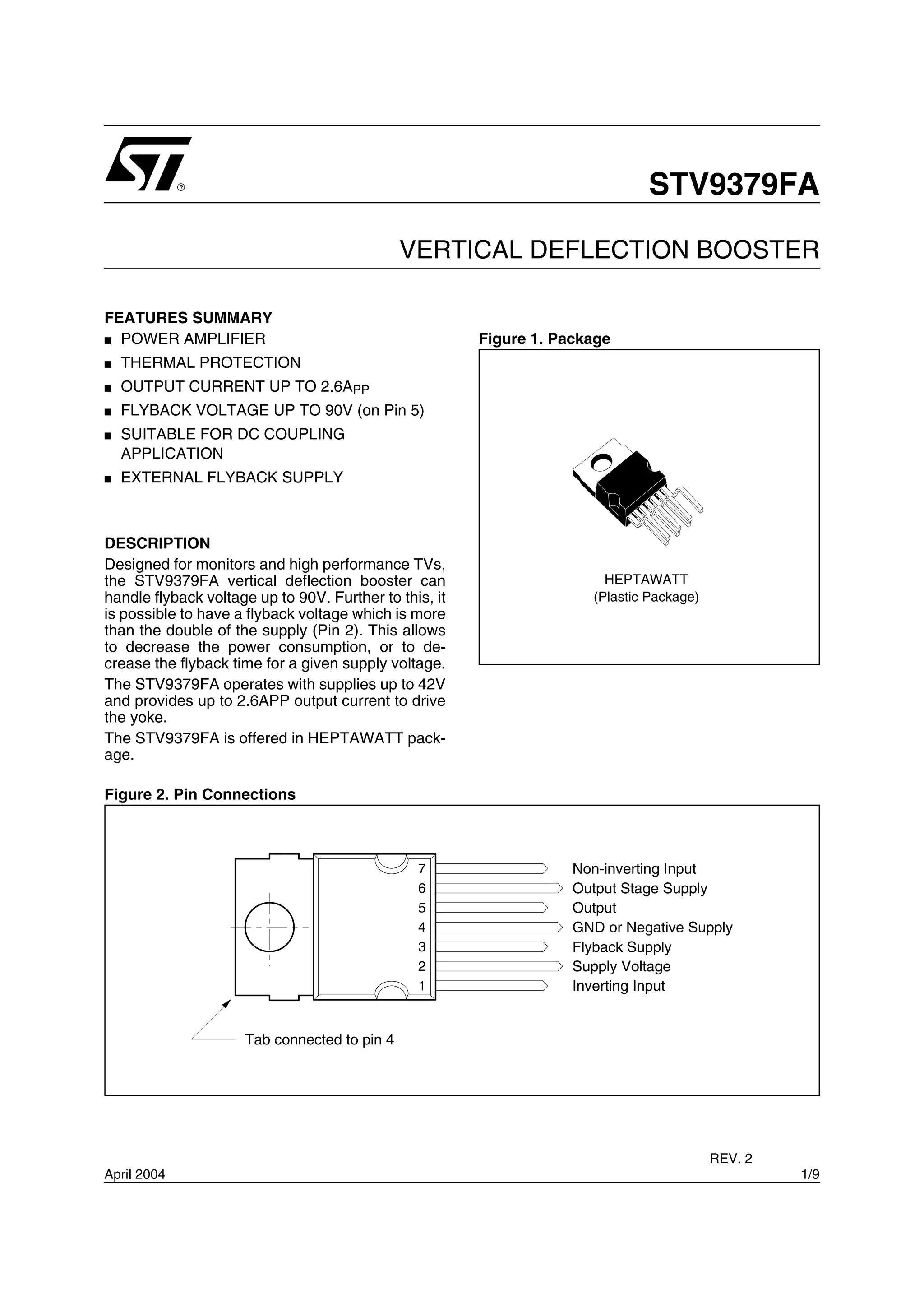
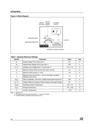

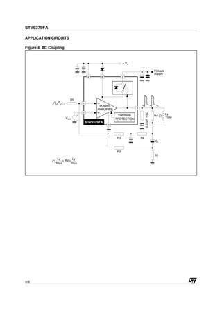

The document summarizes a vertical deflection booster integrated circuit. It can handle flyback voltages up to 90V and provides up to 2.6A of output current. It has thermal protection and can operate with power supply voltages up to 42V. The document includes application examples, electrical specifications, and packaging details.