SlideShare a Scribd company logo
1 of 3
COVER STORY

Detecting failure modes
                                                                                                                                                 endless diversity in form and function of the devices. Each type of device
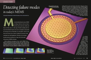
                                                                                           Figure 2: Wyko NT profiler image
                                                                                                                                                 has different complexity in the manufacturing process, a different geometry
                                                                                           of a MeMS fabricated microphone.
                                                                                                    (Courtesy of of Texas Knowles Acoustics)
                                                                                                                                                 (from tens of microns to tens of millimeters in width), and vastly different
                                                                                                                                                 performance requirements or designed responses to external stimuli. Thus,
                                                                                                                                                 while curvature, surface roughness, and switching time may be critical for


in today’s MEMS
                                                                                                                                                   micromirror arrays, co-planarity of the capacitor parts and linewidths
                                                                                                                                                             may be the most crucial parameters for an accelerometer. Initial
                                                                                                                                                                        or long-term failure of a device may also be driven
                                                                                                                                                                                  by an array of factors, such as geometric
                                                                                                                                                                                            errors in production, contamina-
                                                                                                                                                                                                      tion, improper removal
by Noushin Dowlatshahi and Bob Chanapan, Veeco instruments inc.


 M                              icroelectricalmechanical systems (MEMS)

                                are taking a whole new role in our day-to-

                                day life, and are much more widely used

than ever before, due to a wide range of benefits including their low

mass, fast mechanical response, low power consumption, and potential

for lowering end costs. Meanwhile, test and quality control of such

devices has become more critical to facilitate the insertion of this

technology into critical applications. Therefore, it is not surpris-
                                                                                                                                                                                                                of sacrificial
ing that precision metrology has a huge role in this steady                                                                                                                                                    layers, stiction,
                                                                                                                                                                                                              environmental
advancement of MEMS technology.                                                                                                                                                                              attack, fatigue,
                                                                                                                                                                                                            electrostatic
   Unlike traditional semiconductor devices, today’s MEMS devices                                                                                                                                          clamping, fusing,
require characterization in both their static state and under actuation.                                                                                                                                  delamination, or
Parameters of interest include shape, dimensions, surface roughness, side-                                                                                                                              electrical damage.
wall angles, film thickness, residual stress, feature volumes, response times,                                                                                                                            During research
thermal properties, resonance frequencies, stiction, environmental compat-                                                                                                                            and development, there
ibility, and more. The greatest difficulty in MEMS metrology is the nearly                                                                                                                          is also a need to map the
                                                                                                                                                                                                  behavior of devices and
                                                                                                                                                                                                 materials placed under
                                                                                                                                                                                                external stresses (e.g., tem-
                                                                                                                                                                                               perature, pressure, or corro-
                                                                                 Figure 1: Wyko NT
                                                                                                                                                                                              sive agents) in order to fully
                                                                                 dynamic measurement
                                                                                                                                                                                             understand the time-course
                                                                                 reveals a hidden defect
                                                                                 in a micro-mirror.
                                                                                                                                                                                            evolution of these processes.
                                                                                 (Courtesy of of Texas Tech University)
                                                                                                                                                                                           Early detection of failure modes
                                                                                                                                                                                          not only enables improvement at


18 November/December 2008                                                                                                                                                                                                  19
                                                                                                                                                                                           November/December    2008
                              www.smalltimes.com | SMALL TiMeS                                                                 www.smalltimes.                                      com
                                                                                                       SMALL TiMeS |
Early detection
                                                                                                                                      of failure modes
                                                                                                                                      not only enables
                                                                                                                                      improvement at the
                                                                                                                                      next fabrication
                                                                                                                                      cycle and increased
                                                                                                                                      yields, but it
                                                                                                                                      also identifies
the next fabrication cycle and increased yields, but it also      These arrays typically consist of simple cantilever beams,                                              has pros and cons, and         thus the velocity of the moving part. Displacement can also
identifies whether the problem is isolated or systematic,         torsion beams, tethered (piston-style) beams, circular mem-                                             selecting the proper solu-     be measured through integration of this signal. These sys-
                                                                                                                                      whether the
directly impacting field failure quality control.                 branes, and oval membranes. One technique of fabricating                                                tion depends on a number       tems are very sensitive to motion, with sub-nanometer reso-
                                                                  the micromirrors is to use low-temperature adhesive wafer                                               of factors, from device type   lution in the direction perpendicular to the test beam. More
                                                                                                                                      problem is isolated
                                                                  bonding to deposit a thin layer of monocrystalline silicon                                              to stage of manufacturing.     sophisticated systems enable the measurement point to be
RF MeMS
MEMS applications in the domain of radio-frequency (RF)           device to a CMOS wafer. The digital micromirror device                                                      SEMs generally offer the   scanned across the surface, to build up a complete picture of
                                                                                                                                      or systematic,
circuits serve as a perfect example. For certain capaci-          (DMD) developed by Texas Instruments, which incorporates                                                highest lateral resolution     the MEMS out-of-plane motion, though phase information
tive MEMS switches, it is crucial to examine the stiction         more than 500,000 individually addressable micromirrors, has                                            available for static MEMS      between each of the monitoring points is lost due to the time
                                                                                                                                      directly impacting
between the metal layer (top electrode) and the dielectric        made great strides in both performance and reliability of such                                          imaging. These systems         lag between measurements. The lasers on these systems can
layer covering the bottom electrode. The charge build-up          devices. Digital light processing technology based on DMD                                               operate by focusing a beam     also be coupled to other optical systems directly or via fiber
                                                                                                                                      field failure
in the dielectric material can result in what would typi-         has been used in such diverse products as projection displays                                           of electrons on a small area   options, such as stroboscopic bright-field microscopes, so one
cally be called a “failure mode.” The actuation voltage is        with film-like projected images and photographic-quality                                                and detecting the electrons    can get the in-plane-motion through a separate series of mea-
                                                                                                                                      quality control.
directly affecting this charge build-up. Researchers need         printers. Reliability testing of the DMD has demonstrated                                               that are scattered from the    surements with that equip-
to understand how an increase or decrease in the actua-           greater than 100,000 operating hours and more than 1 tril-                                              surface. Measurement time      ment. However, all systems are
                                                                                                                                                                                                                                                 Manufacturers
tion voltage can impact the lifetime of typical MEMS. This        lion mirror cycles.                                                                                     is typically between 5–10s     sensitive to the roughness of
actuation voltage is typically related to the device geometry,        It is crucial for micromirror array manufacturers to exam-                                          after the sample has been      the surface, requiring enough
                                                                                                                                                                                                                                                 have relied on a
mechanical and material properties, and residual stresses         ine the uniformity in how the micromirrors tilt in an array,                                            loaded into the system.        light to be scattered back into
in the devices. When voltage is applied to a typical capaci-      the time it takes them to tilt, and how repeatable this behav-      Lateral resolutions down to the nanometer level are possible,      the detector for adequate sig-
                                                                                                                                                                                                                                                 range of methods
tive RF MEMS switch, the electrostatic charges cause a dis-       ior is. This is in addition to the traditional parameters of mir-   and depth-of-focus of such systems can be quite large. SEMs        nal-to-noise. Therefore, very
tributed electrostatic force, leading to deformation of the       ror curvature/deflection angle roughness and surface topog-         provide an invaluable tool for evaluating sidewall angles and      smooth or rough surfaces can
                                                                                                                                                                                                                                                 to identify
micro-structure. Later, due to the storage of elastic energy,     raphy. Moreover, as the devices are packaged in hermetically        roughness of very steep parts, and are often the only systems      degrade accuracy.
the structure tends to return to its original state. Accurate     sealed packages, the encapsulation process can further affect       capable of these measurements in such applications as micro-           Digital holography (DH)
                                                                                                                                                                                                                                                 structural failure
metrology can play a significant role in characterizing such a    the operational performance. Environmental factors includ-          fluidics and capacitive accelerometers. The primary limitations    has been employed for many
switch by defining and evaluating the membrane’s deforma-         ing temperature and humidity also impact on such devices,           of the technique are that samples must be placed in vacuum,        years to measure vibrating
                                                                                                                                                                                                                                                 modes in MEMS.
tion and analyzing thermal impact, as well as the material        creating the need of a fourth-dimensional capable, non-con-         and the penetration depth of electrons is very small, limiting     devices. In this technique,
and mechanical properties of the metal.                           tact metrology solution. Inspecting the device in a meaning-        effective analysis on packaged parts. Also, parts must often       a digital camera is used to
                                                                  ful manner can monitor and minimize fabrication errors and          be cross-sectioned in order to achieve the proper orientation      record a hologram produced
                                                                  positively impact the micromirrors components within an             for best measurement, which can be cost prohibitive. Lastly,       by interfering a high-quality reference beam with a beam
Micromirrors
Another widely used type of MEMS device that exhibits             array.                                                              edges may produce artifacts if they become charged, leading        reflected from the sample under test. As the test object is later
particular metrology needs is the micromirror array, which                                                                            to inaccurate data.                                                deformed, the modified object beam is compared with the
is finding use in adaptive optics for both space and consumer                                                                             Laser Doppler vibrometers are frequently used for rapid        original digitally recorded hologram, and the deformation can
                                                                  inspection strategies
electronics, as well as in projectors, televisions, and digital   Manufacturers have relied on a range of methods to iden-            characterization of out-of-plane MEMS motion. These sys-           be quantified using standard phase-shifting or other interfero-
cameras. These mirror devices must be 100% reliable and           tify structural failure modes in MEMS: optical microscopy,          tems employ a beam of modulated laser light that is reflected      metric techniques. These systems can therefore achieve nano-
accurate. Because of variations in device geometry that result    stylus profilometrey, infrared (IR) thermal imaging, focused        from the moving test piece. The returned light is Doppler-         meter-level measurement of out-of-plane motion of devices.
from the micro-fabrication process, the performance from one      ion beams (FIB), scanning electron microscopy (SEM), digital        shifted from the original modulated beam, and the two beams        Using high-speed cameras, deformations of up to several thou-
device to the next can vary, making it difficult to reliably      holography (DH), atomic force microscopy (AFM), and trans-          are then compared. A spectrum analyzer or other electronics        sand hertz can be measured. The systems can also be com-
ensure accuracy and repeatability of the actuator positions.      mission electron microscopy (TEM). Each of these techniques         can be used to determine the magnitude of the shift, and           bined with stroboscopic methods to measure motions up to


20 November/December 2008                                                                                                                                                                                                                                            21
                                                                                                                                                                                                                                       November/December 2008
                                   www.smalltimes.com | SMALL TiMeS                                                                                                                                          www.smalltimes.com
                                                                                                                                                                                            SMALL TiMeS |
It is now possible
                            to perform
                            non-destructive,
                            rapid, extremely
                            precise MEMS
                            characterization
                            through packaging
                            and under operation
several megahertz,                                                  to the device under test and the other part to a high-quality
similar to the strobed                                              reference surface. The light recombines to form a pattern of
                            on a single
systems mentioned                                                   interference “fringes.” The reference surface is then trans-
previously. Like the                                                lated relative to the test surface, and multiple frames of data
                            measuring tool.
other optical meth-                                                 are obtained during the translation. The resulting series of
ods, digital holo-                                                  fringe patterns are analyzed to calculate the surface profiler of
graphic systems can                                                 the device. Optical profilers provide rapid, 3-D, non-contact
measure parts through a transparent cover glass. How-               sample surface characterization. Consequently, this method
ever, as the source employed is a laser with long coher-            has proven quite useful for MEMS production processes. How-
ence length, they can suffer speckle problems from diffuse          ever, this method has traditionally also been inadequate for
MEMS surfaces and may also have problems with transpar-             determining a device’s dynamic ability to perform, such as
ent films on a surface.                                             actuation, deformation, rotation, etc.
   Atomic force microscopes (AFM) employ nanoscale tips                 CalTech overcame this primary limitation of optical pro-
attached to the end of a cantilever that is brought very close      filing by combining it with stroboscopic illumination for
to the test surface. Measurement of the tip deflection allows       dynamic measurement of MEMS devices in motion. Strobo-
full 3-D characterization of the surface, and van der Waals         scopic illumination effectively “freezes” the motion of MEMS
forces between the tip and sample can be detected. AFMs             structures, allowing nanometer-resolution measurement of
utilize a variety of measurement modes, including “contact          their surface shape. By varying the amplitude, phase, and
mode” (where the tip lightly touches the sample) and “tap-          frequency of the drive signal, multiple measurements can be
ping mode” (where high-frequency tip oscillations are used          taken to describe the device’s full range of actuation/defor-
to minimize contact with the sample while maintaining the           mation. Moving MEMS structures can then be analyzed for
high signal-to-noise ratio). AFMs have the highest lateral          flatness variation, tilt, lateral translation, linearity of motion,
and vertical resolutions available of any three-dimensional         stiction, and other key device parameters.
metrology instrumentation, with sub-nanometer features                  Today’s top-of-the-line optical profilers incorporate this
visible in all three dimensions. However, the field of view         technology along with other advances to provide a best mea-
for a scan is typically only about 120µm2, and vertical limits      surement solution for MEMS researchers and manufacturers.
are about 10µm in height. In addition, AFM measurements             Veeco’s ninth-generation Wyko NT profilers incorporate LED
are relatively slow. Due to the scan speed and contact nature       illumination for higher light levels and In-Motion capability for
of the scan, these systems are incapable of measuring MEMS          measuring devices under actuation from 0–2.4mHz with ang-
while under actuation.                                              strom-level resolution. Objective modules that can visualize
    Optical profiling (white light interferometry) has long         parts through packaging are also commercially available.
served as a standard technique for measuring surface topog-             Thus, it is now possible to perform non-destructive, rapid,
raphy of MEMS and optical MEMS devices. In a white-light            extremely precise MEMS characterization through packaging
optical microscope, the illumination source is traditionally a      and under operation on a single measuring tool.
tungsten-halogen bulb, coupled into an optical system with
several interferometric microscope objectives. Light from the       NoushiN Dowlatshahi is marketing product engineer at Veeco Instruments
                                                                    Inc. Bob Chanapan is marketing product manager at Veeco Instruments Inc.
source is split in the objective, with part of the beam traveling


22 November/December 2008           www.smalltimes.com | SMALL TiMeS

More Related Content

Similar to SmallTimes

Mems reliability & failure mechanisms
Mems reliability & failure mechanismsMems reliability & failure mechanisms
Mems reliability & failure mechanismsDeepak Xavier
 
Ep&t article
Ep&t articleEp&t article
Ep&t articleShimifrez
 
Testo thermography on photovoltaic_sysems 2012
Testo thermography on photovoltaic_sysems 2012Testo thermography on photovoltaic_sysems 2012
Testo thermography on photovoltaic_sysems 2012Testo Limited
 
Review on evaluation mechanical properties of materials for mems
Review on evaluation mechanical properties  of materials for memsReview on evaluation mechanical properties  of materials for mems
Review on evaluation mechanical properties of materials for memsnagesh sharma
 
Mems Reliability Review
Mems Reliability ReviewMems Reliability Review
Mems Reliability ReviewAnil Bharadwaj
 
Numerical modelling in Geomechanics
Numerical modelling in GeomechanicsNumerical modelling in Geomechanics
Numerical modelling in GeomechanicsUlimella Siva Sankar
 
IRJET- Fabrication, Sensing and Applications of NEMS/MEMS Technology
IRJET- Fabrication, Sensing and Applications of NEMS/MEMS TechnologyIRJET- Fabrication, Sensing and Applications of NEMS/MEMS Technology
IRJET- Fabrication, Sensing and Applications of NEMS/MEMS TechnologyIRJET Journal
 
PAPER ON MEMS TECHNOLOGY
PAPER ON MEMS TECHNOLOGYPAPER ON MEMS TECHNOLOGY
PAPER ON MEMS TECHNOLOGYDhaval Kaneria
 
Static structural and dynamic analysis of cracks in composite materials
Static structural and dynamic analysis of cracks in composite materialsStatic structural and dynamic analysis of cracks in composite materials
Static structural and dynamic analysis of cracks in composite materialsIRJET Journal
 
Mems stiction and anti stiction
Mems stiction and anti stictionMems stiction and anti stiction
Mems stiction and anti stictionkhalil226
 
Mesh radio based ami solution robulink
Mesh radio based ami solution robulinkMesh radio based ami solution robulink
Mesh radio based ami solution robulinkjessie968
 
MSc rjfg V1
MSc rjfg V1MSc rjfg V1
MSc rjfg V1rodofg
 
Design challenges in physical design
Design challenges in physical designDesign challenges in physical design
Design challenges in physical designDeiptii Das
 
ADVANCED ALGORITHMS FOR ETCHING SIMULATION OF 3D MEMS-TUNABLE LASERS
ADVANCED ALGORITHMS FOR ETCHING SIMULATION OF 3D MEMS-TUNABLE LASERSADVANCED ALGORITHMS FOR ETCHING SIMULATION OF 3D MEMS-TUNABLE LASERS
ADVANCED ALGORITHMS FOR ETCHING SIMULATION OF 3D MEMS-TUNABLE LASERSijctcm
 
Seminar on Electrochemical Surface Structuring
Seminar on Electrochemical Surface StructuringSeminar on Electrochemical Surface Structuring
Seminar on Electrochemical Surface StructuringSRINJOY GUHA
 
Influence of gate geometry in integrated mos varactors on accumulation mode f...
Influence of gate geometry in integrated mos varactors on accumulation mode f...Influence of gate geometry in integrated mos varactors on accumulation mode f...
Influence of gate geometry in integrated mos varactors on accumulation mode f...RFIC-IUMA
 

Similar to SmallTimes (20)

Mems reliability & failure mechanisms
Mems reliability & failure mechanismsMems reliability & failure mechanisms
Mems reliability & failure mechanisms
 
Ep&t article
Ep&t articleEp&t article
Ep&t article
 
Testo thermography on photovoltaic_sysems 2012
Testo thermography on photovoltaic_sysems 2012Testo thermography on photovoltaic_sysems 2012
Testo thermography on photovoltaic_sysems 2012
 
Review on evaluation mechanical properties of materials for mems
Review on evaluation mechanical properties  of materials for memsReview on evaluation mechanical properties  of materials for mems
Review on evaluation mechanical properties of materials for mems
 
Mems Reliability Review
Mems Reliability ReviewMems Reliability Review
Mems Reliability Review
 
numerical model
numerical modelnumerical model
numerical model
 
Numerical modelling in Geomechanics
Numerical modelling in GeomechanicsNumerical modelling in Geomechanics
Numerical modelling in Geomechanics
 
IRJET- Fabrication, Sensing and Applications of NEMS/MEMS Technology
IRJET- Fabrication, Sensing and Applications of NEMS/MEMS TechnologyIRJET- Fabrication, Sensing and Applications of NEMS/MEMS Technology
IRJET- Fabrication, Sensing and Applications of NEMS/MEMS Technology
 
Features measurement analysis of pull-in voltage for embedded MEMS
Features measurement analysis of pull-in voltage for embedded  MEMSFeatures measurement analysis of pull-in voltage for embedded  MEMS
Features measurement analysis of pull-in voltage for embedded MEMS
 
PAPER ON MEMS TECHNOLOGY
PAPER ON MEMS TECHNOLOGYPAPER ON MEMS TECHNOLOGY
PAPER ON MEMS TECHNOLOGY
 
Static structural and dynamic analysis of cracks in composite materials
Static structural and dynamic analysis of cracks in composite materialsStatic structural and dynamic analysis of cracks in composite materials
Static structural and dynamic analysis of cracks in composite materials
 
Mems stiction and anti stiction
Mems stiction and anti stictionMems stiction and anti stiction
Mems stiction and anti stiction
 
Ases Paper 2011
Ases Paper 2011Ases Paper 2011
Ases Paper 2011
 
Mesh radio based ami solution robulink
Mesh radio based ami solution robulinkMesh radio based ami solution robulink
Mesh radio based ami solution robulink
 
MSc rjfg V1
MSc rjfg V1MSc rjfg V1
MSc rjfg V1
 
Design challenges in physical design
Design challenges in physical designDesign challenges in physical design
Design challenges in physical design
 
Master Report
Master ReportMaster Report
Master Report
 
ADVANCED ALGORITHMS FOR ETCHING SIMULATION OF 3D MEMS-TUNABLE LASERS
ADVANCED ALGORITHMS FOR ETCHING SIMULATION OF 3D MEMS-TUNABLE LASERSADVANCED ALGORITHMS FOR ETCHING SIMULATION OF 3D MEMS-TUNABLE LASERS
ADVANCED ALGORITHMS FOR ETCHING SIMULATION OF 3D MEMS-TUNABLE LASERS
 
Seminar on Electrochemical Surface Structuring
Seminar on Electrochemical Surface StructuringSeminar on Electrochemical Surface Structuring
Seminar on Electrochemical Surface Structuring
 
Influence of gate geometry in integrated mos varactors on accumulation mode f...
Influence of gate geometry in integrated mos varactors on accumulation mode f...Influence of gate geometry in integrated mos varactors on accumulation mode f...
Influence of gate geometry in integrated mos varactors on accumulation mode f...
 

More from ta_ha_nuk

More Notes 11.05.09
More Notes 11.05.09More Notes 11.05.09
More Notes 11.05.09ta_ha_nuk
 
Pine Hill Ads
Pine Hill AdsPine Hill Ads
Pine Hill Adsta_ha_nuk
 
Industrial Laser Solutions
Industrial Laser SolutionsIndustrial Laser Solutions
Industrial Laser Solutionsta_ha_nuk
 
Electronic Publishing
Electronic PublishingElectronic Publishing
Electronic Publishingta_ha_nuk
 
Industrial Laser Solutions
Industrial Laser SolutionsIndustrial Laser Solutions
Industrial Laser Solutionsta_ha_nuk
 
Industrial Laser Solutions
Industrial Laser SolutionsIndustrial Laser Solutions
Industrial Laser Solutionsta_ha_nuk
 
Electronic Publishing
Electronic PublishingElectronic Publishing
Electronic Publishingta_ha_nuk
 

More from ta_ha_nuk (7)

More Notes 11.05.09
More Notes 11.05.09More Notes 11.05.09
More Notes 11.05.09
 
Pine Hill Ads
Pine Hill AdsPine Hill Ads
Pine Hill Ads
 
Industrial Laser Solutions
Industrial Laser SolutionsIndustrial Laser Solutions
Industrial Laser Solutions
 
Electronic Publishing
Electronic PublishingElectronic Publishing
Electronic Publishing
 
Industrial Laser Solutions
Industrial Laser SolutionsIndustrial Laser Solutions
Industrial Laser Solutions
 
Industrial Laser Solutions
Industrial Laser SolutionsIndustrial Laser Solutions
Industrial Laser Solutions
 
Electronic Publishing
Electronic PublishingElectronic Publishing
Electronic Publishing
 

Recently uploaded

SIEMENS: RAPUNZEL – A Tale About Knowledge Graph
SIEMENS: RAPUNZEL – A Tale About Knowledge GraphSIEMENS: RAPUNZEL – A Tale About Knowledge Graph
SIEMENS: RAPUNZEL – A Tale About Knowledge GraphNeo4j
 
Advanced Test Driven-Development @ php[tek] 2024
Advanced Test Driven-Development @ php[tek] 2024Advanced Test Driven-Development @ php[tek] 2024
Advanced Test Driven-Development @ php[tek] 2024Scott Keck-Warren
 
Swan(sea) Song – personal research during my six years at Swansea ... and bey...
Swan(sea) Song – personal research during my six years at Swansea ... and bey...Swan(sea) Song – personal research during my six years at Swansea ... and bey...
Swan(sea) Song – personal research during my six years at Swansea ... and bey...Alan Dix
 
CloudStudio User manual (basic edition):
CloudStudio User manual (basic edition):CloudStudio User manual (basic edition):
CloudStudio User manual (basic edition):comworks
 
Transcript: New from BookNet Canada for 2024: BNC BiblioShare - Tech Forum 2024
Transcript: New from BookNet Canada for 2024: BNC BiblioShare - Tech Forum 2024Transcript: New from BookNet Canada for 2024: BNC BiblioShare - Tech Forum 2024
Transcript: New from BookNet Canada for 2024: BNC BiblioShare - Tech Forum 2024BookNet Canada
 
Are Multi-Cloud and Serverless Good or Bad?
Are Multi-Cloud and Serverless Good or Bad?Are Multi-Cloud and Serverless Good or Bad?
Are Multi-Cloud and Serverless Good or Bad?Mattias Andersson
 
#StandardsGoals for 2024: What’s new for BISAC - Tech Forum 2024
#StandardsGoals for 2024: What’s new for BISAC - Tech Forum 2024#StandardsGoals for 2024: What’s new for BISAC - Tech Forum 2024
#StandardsGoals for 2024: What’s new for BISAC - Tech Forum 2024BookNet Canada
 
Kotlin Multiplatform & Compose Multiplatform - Starter kit for pragmatics
Kotlin Multiplatform & Compose Multiplatform - Starter kit for pragmaticsKotlin Multiplatform & Compose Multiplatform - Starter kit for pragmatics
Kotlin Multiplatform & Compose Multiplatform - Starter kit for pragmaticsAndrey Dotsenko
 
Bluetooth Controlled Car with Arduino.pdf
Bluetooth Controlled Car with Arduino.pdfBluetooth Controlled Car with Arduino.pdf
Bluetooth Controlled Car with Arduino.pdfngoud9212
 
Understanding the Laravel MVC Architecture
Understanding the Laravel MVC ArchitectureUnderstanding the Laravel MVC Architecture
Understanding the Laravel MVC ArchitecturePixlogix Infotech
 
My Hashitalk Indonesia April 2024 Presentation
My Hashitalk Indonesia April 2024 PresentationMy Hashitalk Indonesia April 2024 Presentation
My Hashitalk Indonesia April 2024 PresentationRidwan Fadjar
 
Pigging Solutions Piggable Sweeping Elbows
Pigging Solutions Piggable Sweeping ElbowsPigging Solutions Piggable Sweeping Elbows
Pigging Solutions Piggable Sweeping ElbowsPigging Solutions
 
AI as an Interface for Commercial Buildings
AI as an Interface for Commercial BuildingsAI as an Interface for Commercial Buildings
AI as an Interface for Commercial BuildingsMemoori
 
Transcript: #StandardsGoals for 2024: What’s new for BISAC - Tech Forum 2024
Transcript: #StandardsGoals for 2024: What’s new for BISAC - Tech Forum 2024Transcript: #StandardsGoals for 2024: What’s new for BISAC - Tech Forum 2024
Transcript: #StandardsGoals for 2024: What’s new for BISAC - Tech Forum 2024BookNet Canada
 
"LLMs for Python Engineers: Advanced Data Analysis and Semantic Kernel",Oleks...
"LLMs for Python Engineers: Advanced Data Analysis and Semantic Kernel",Oleks..."LLMs for Python Engineers: Advanced Data Analysis and Semantic Kernel",Oleks...
"LLMs for Python Engineers: Advanced Data Analysis and Semantic Kernel",Oleks...Fwdays
 
Bun (KitWorks Team Study 노별마루 발표 2024.4.22)
Bun (KitWorks Team Study 노별마루 발표 2024.4.22)Bun (KitWorks Team Study 노별마루 발표 2024.4.22)
Bun (KitWorks Team Study 노별마루 발표 2024.4.22)Wonjun Hwang
 
Snow Chain-Integrated Tire for a Safe Drive on Winter Roads
Snow Chain-Integrated Tire for a Safe Drive on Winter RoadsSnow Chain-Integrated Tire for a Safe Drive on Winter Roads
Snow Chain-Integrated Tire for a Safe Drive on Winter RoadsHyundai Motor Group
 
Tech-Forward - Achieving Business Readiness For Copilot in Microsoft 365
Tech-Forward - Achieving Business Readiness For Copilot in Microsoft 365Tech-Forward - Achieving Business Readiness For Copilot in Microsoft 365
Tech-Forward - Achieving Business Readiness For Copilot in Microsoft 3652toLead Limited
 
SQL Database Design For Developers at php[tek] 2024
SQL Database Design For Developers at php[tek] 2024SQL Database Design For Developers at php[tek] 2024
SQL Database Design For Developers at php[tek] 2024Scott Keck-Warren
 

Recently uploaded (20)

SIEMENS: RAPUNZEL – A Tale About Knowledge Graph
SIEMENS: RAPUNZEL – A Tale About Knowledge GraphSIEMENS: RAPUNZEL – A Tale About Knowledge Graph
SIEMENS: RAPUNZEL – A Tale About Knowledge Graph
 
Hot Sexy call girls in Panjabi Bagh 🔝 9953056974 🔝 Delhi escort Service
Hot Sexy call girls in Panjabi Bagh 🔝 9953056974 🔝 Delhi escort ServiceHot Sexy call girls in Panjabi Bagh 🔝 9953056974 🔝 Delhi escort Service
Hot Sexy call girls in Panjabi Bagh 🔝 9953056974 🔝 Delhi escort Service
 
Advanced Test Driven-Development @ php[tek] 2024
Advanced Test Driven-Development @ php[tek] 2024Advanced Test Driven-Development @ php[tek] 2024
Advanced Test Driven-Development @ php[tek] 2024
 
Swan(sea) Song – personal research during my six years at Swansea ... and bey...
Swan(sea) Song – personal research during my six years at Swansea ... and bey...Swan(sea) Song – personal research during my six years at Swansea ... and bey...
Swan(sea) Song – personal research during my six years at Swansea ... and bey...
 
CloudStudio User manual (basic edition):
CloudStudio User manual (basic edition):CloudStudio User manual (basic edition):
CloudStudio User manual (basic edition):
 
Transcript: New from BookNet Canada for 2024: BNC BiblioShare - Tech Forum 2024
Transcript: New from BookNet Canada for 2024: BNC BiblioShare - Tech Forum 2024Transcript: New from BookNet Canada for 2024: BNC BiblioShare - Tech Forum 2024
Transcript: New from BookNet Canada for 2024: BNC BiblioShare - Tech Forum 2024
 
Are Multi-Cloud and Serverless Good or Bad?
Are Multi-Cloud and Serverless Good or Bad?Are Multi-Cloud and Serverless Good or Bad?
Are Multi-Cloud and Serverless Good or Bad?
 
#StandardsGoals for 2024: What’s new for BISAC - Tech Forum 2024
#StandardsGoals for 2024: What’s new for BISAC - Tech Forum 2024#StandardsGoals for 2024: What’s new for BISAC - Tech Forum 2024
#StandardsGoals for 2024: What’s new for BISAC - Tech Forum 2024
 
Kotlin Multiplatform & Compose Multiplatform - Starter kit for pragmatics
Kotlin Multiplatform & Compose Multiplatform - Starter kit for pragmaticsKotlin Multiplatform & Compose Multiplatform - Starter kit for pragmatics
Kotlin Multiplatform & Compose Multiplatform - Starter kit for pragmatics
 
Bluetooth Controlled Car with Arduino.pdf
Bluetooth Controlled Car with Arduino.pdfBluetooth Controlled Car with Arduino.pdf
Bluetooth Controlled Car with Arduino.pdf
 
Understanding the Laravel MVC Architecture
Understanding the Laravel MVC ArchitectureUnderstanding the Laravel MVC Architecture
Understanding the Laravel MVC Architecture
 
My Hashitalk Indonesia April 2024 Presentation
My Hashitalk Indonesia April 2024 PresentationMy Hashitalk Indonesia April 2024 Presentation
My Hashitalk Indonesia April 2024 Presentation
 
Pigging Solutions Piggable Sweeping Elbows
Pigging Solutions Piggable Sweeping ElbowsPigging Solutions Piggable Sweeping Elbows
Pigging Solutions Piggable Sweeping Elbows
 
AI as an Interface for Commercial Buildings
AI as an Interface for Commercial BuildingsAI as an Interface for Commercial Buildings
AI as an Interface for Commercial Buildings
 
Transcript: #StandardsGoals for 2024: What’s new for BISAC - Tech Forum 2024
Transcript: #StandardsGoals for 2024: What’s new for BISAC - Tech Forum 2024Transcript: #StandardsGoals for 2024: What’s new for BISAC - Tech Forum 2024
Transcript: #StandardsGoals for 2024: What’s new for BISAC - Tech Forum 2024
 
"LLMs for Python Engineers: Advanced Data Analysis and Semantic Kernel",Oleks...
"LLMs for Python Engineers: Advanced Data Analysis and Semantic Kernel",Oleks..."LLMs for Python Engineers: Advanced Data Analysis and Semantic Kernel",Oleks...
"LLMs for Python Engineers: Advanced Data Analysis and Semantic Kernel",Oleks...
 
Bun (KitWorks Team Study 노별마루 발표 2024.4.22)
Bun (KitWorks Team Study 노별마루 발표 2024.4.22)Bun (KitWorks Team Study 노별마루 발표 2024.4.22)
Bun (KitWorks Team Study 노별마루 발표 2024.4.22)
 
Snow Chain-Integrated Tire for a Safe Drive on Winter Roads
Snow Chain-Integrated Tire for a Safe Drive on Winter RoadsSnow Chain-Integrated Tire for a Safe Drive on Winter Roads
Snow Chain-Integrated Tire for a Safe Drive on Winter Roads
 
Tech-Forward - Achieving Business Readiness For Copilot in Microsoft 365
Tech-Forward - Achieving Business Readiness For Copilot in Microsoft 365Tech-Forward - Achieving Business Readiness For Copilot in Microsoft 365
Tech-Forward - Achieving Business Readiness For Copilot in Microsoft 365
 
SQL Database Design For Developers at php[tek] 2024
SQL Database Design For Developers at php[tek] 2024SQL Database Design For Developers at php[tek] 2024
SQL Database Design For Developers at php[tek] 2024
 

SmallTimes

  • 1. COVER STORY Detecting failure modes endless diversity in form and function of the devices. Each type of device Figure 2: Wyko NT profiler image has different complexity in the manufacturing process, a different geometry of a MeMS fabricated microphone. (Courtesy of of Texas Knowles Acoustics) (from tens of microns to tens of millimeters in width), and vastly different performance requirements or designed responses to external stimuli. Thus, while curvature, surface roughness, and switching time may be critical for in today’s MEMS micromirror arrays, co-planarity of the capacitor parts and linewidths may be the most crucial parameters for an accelerometer. Initial or long-term failure of a device may also be driven by an array of factors, such as geometric errors in production, contamina- tion, improper removal by Noushin Dowlatshahi and Bob Chanapan, Veeco instruments inc. M icroelectricalmechanical systems (MEMS) are taking a whole new role in our day-to- day life, and are much more widely used than ever before, due to a wide range of benefits including their low mass, fast mechanical response, low power consumption, and potential for lowering end costs. Meanwhile, test and quality control of such devices has become more critical to facilitate the insertion of this technology into critical applications. Therefore, it is not surpris- of sacrificial ing that precision metrology has a huge role in this steady layers, stiction, environmental advancement of MEMS technology. attack, fatigue, electrostatic Unlike traditional semiconductor devices, today’s MEMS devices clamping, fusing, require characterization in both their static state and under actuation. delamination, or Parameters of interest include shape, dimensions, surface roughness, side- electrical damage. wall angles, film thickness, residual stress, feature volumes, response times, During research thermal properties, resonance frequencies, stiction, environmental compat- and development, there ibility, and more. The greatest difficulty in MEMS metrology is the nearly is also a need to map the behavior of devices and materials placed under external stresses (e.g., tem- perature, pressure, or corro- Figure 1: Wyko NT sive agents) in order to fully dynamic measurement understand the time-course reveals a hidden defect in a micro-mirror. evolution of these processes. (Courtesy of of Texas Tech University) Early detection of failure modes not only enables improvement at 18 November/December 2008 19 November/December 2008 www.smalltimes.com | SMALL TiMeS www.smalltimes. com SMALL TiMeS |
  • 2. Early detection of failure modes not only enables improvement at the next fabrication cycle and increased yields, but it also identifies the next fabrication cycle and increased yields, but it also These arrays typically consist of simple cantilever beams, has pros and cons, and thus the velocity of the moving part. Displacement can also identifies whether the problem is isolated or systematic, torsion beams, tethered (piston-style) beams, circular mem- selecting the proper solu- be measured through integration of this signal. These sys- whether the directly impacting field failure quality control. branes, and oval membranes. One technique of fabricating tion depends on a number tems are very sensitive to motion, with sub-nanometer reso- the micromirrors is to use low-temperature adhesive wafer of factors, from device type lution in the direction perpendicular to the test beam. More problem is isolated bonding to deposit a thin layer of monocrystalline silicon to stage of manufacturing. sophisticated systems enable the measurement point to be RF MeMS MEMS applications in the domain of radio-frequency (RF) device to a CMOS wafer. The digital micromirror device SEMs generally offer the scanned across the surface, to build up a complete picture of or systematic, circuits serve as a perfect example. For certain capaci- (DMD) developed by Texas Instruments, which incorporates highest lateral resolution the MEMS out-of-plane motion, though phase information tive MEMS switches, it is crucial to examine the stiction more than 500,000 individually addressable micromirrors, has available for static MEMS between each of the monitoring points is lost due to the time directly impacting between the metal layer (top electrode) and the dielectric made great strides in both performance and reliability of such imaging. These systems lag between measurements. The lasers on these systems can layer covering the bottom electrode. The charge build-up devices. Digital light processing technology based on DMD operate by focusing a beam also be coupled to other optical systems directly or via fiber field failure in the dielectric material can result in what would typi- has been used in such diverse products as projection displays of electrons on a small area options, such as stroboscopic bright-field microscopes, so one cally be called a “failure mode.” The actuation voltage is with film-like projected images and photographic-quality and detecting the electrons can get the in-plane-motion through a separate series of mea- quality control. directly affecting this charge build-up. Researchers need printers. Reliability testing of the DMD has demonstrated that are scattered from the surements with that equip- to understand how an increase or decrease in the actua- greater than 100,000 operating hours and more than 1 tril- surface. Measurement time ment. However, all systems are Manufacturers tion voltage can impact the lifetime of typical MEMS. This lion mirror cycles. is typically between 5–10s sensitive to the roughness of actuation voltage is typically related to the device geometry, It is crucial for micromirror array manufacturers to exam- after the sample has been the surface, requiring enough have relied on a mechanical and material properties, and residual stresses ine the uniformity in how the micromirrors tilt in an array, loaded into the system. light to be scattered back into in the devices. When voltage is applied to a typical capaci- the time it takes them to tilt, and how repeatable this behav- Lateral resolutions down to the nanometer level are possible, the detector for adequate sig- range of methods tive RF MEMS switch, the electrostatic charges cause a dis- ior is. This is in addition to the traditional parameters of mir- and depth-of-focus of such systems can be quite large. SEMs nal-to-noise. Therefore, very tributed electrostatic force, leading to deformation of the ror curvature/deflection angle roughness and surface topog- provide an invaluable tool for evaluating sidewall angles and smooth or rough surfaces can to identify micro-structure. Later, due to the storage of elastic energy, raphy. Moreover, as the devices are packaged in hermetically roughness of very steep parts, and are often the only systems degrade accuracy. the structure tends to return to its original state. Accurate sealed packages, the encapsulation process can further affect capable of these measurements in such applications as micro- Digital holography (DH) structural failure metrology can play a significant role in characterizing such a the operational performance. Environmental factors includ- fluidics and capacitive accelerometers. The primary limitations has been employed for many switch by defining and evaluating the membrane’s deforma- ing temperature and humidity also impact on such devices, of the technique are that samples must be placed in vacuum, years to measure vibrating modes in MEMS. tion and analyzing thermal impact, as well as the material creating the need of a fourth-dimensional capable, non-con- and the penetration depth of electrons is very small, limiting devices. In this technique, and mechanical properties of the metal. tact metrology solution. Inspecting the device in a meaning- effective analysis on packaged parts. Also, parts must often a digital camera is used to ful manner can monitor and minimize fabrication errors and be cross-sectioned in order to achieve the proper orientation record a hologram produced positively impact the micromirrors components within an for best measurement, which can be cost prohibitive. Lastly, by interfering a high-quality reference beam with a beam Micromirrors Another widely used type of MEMS device that exhibits array. edges may produce artifacts if they become charged, leading reflected from the sample under test. As the test object is later particular metrology needs is the micromirror array, which to inaccurate data. deformed, the modified object beam is compared with the is finding use in adaptive optics for both space and consumer Laser Doppler vibrometers are frequently used for rapid original digitally recorded hologram, and the deformation can inspection strategies electronics, as well as in projectors, televisions, and digital Manufacturers have relied on a range of methods to iden- characterization of out-of-plane MEMS motion. These sys- be quantified using standard phase-shifting or other interfero- cameras. These mirror devices must be 100% reliable and tify structural failure modes in MEMS: optical microscopy, tems employ a beam of modulated laser light that is reflected metric techniques. These systems can therefore achieve nano- accurate. Because of variations in device geometry that result stylus profilometrey, infrared (IR) thermal imaging, focused from the moving test piece. The returned light is Doppler- meter-level measurement of out-of-plane motion of devices. from the micro-fabrication process, the performance from one ion beams (FIB), scanning electron microscopy (SEM), digital shifted from the original modulated beam, and the two beams Using high-speed cameras, deformations of up to several thou- device to the next can vary, making it difficult to reliably holography (DH), atomic force microscopy (AFM), and trans- are then compared. A spectrum analyzer or other electronics sand hertz can be measured. The systems can also be com- ensure accuracy and repeatability of the actuator positions. mission electron microscopy (TEM). Each of these techniques can be used to determine the magnitude of the shift, and bined with stroboscopic methods to measure motions up to 20 November/December 2008 21 November/December 2008 www.smalltimes.com | SMALL TiMeS www.smalltimes.com SMALL TiMeS |
  • 3. It is now possible to perform non-destructive, rapid, extremely precise MEMS characterization through packaging and under operation several megahertz, to the device under test and the other part to a high-quality similar to the strobed reference surface. The light recombines to form a pattern of on a single systems mentioned interference “fringes.” The reference surface is then trans- previously. Like the lated relative to the test surface, and multiple frames of data measuring tool. other optical meth- are obtained during the translation. The resulting series of ods, digital holo- fringe patterns are analyzed to calculate the surface profiler of graphic systems can the device. Optical profilers provide rapid, 3-D, non-contact measure parts through a transparent cover glass. How- sample surface characterization. Consequently, this method ever, as the source employed is a laser with long coher- has proven quite useful for MEMS production processes. How- ence length, they can suffer speckle problems from diffuse ever, this method has traditionally also been inadequate for MEMS surfaces and may also have problems with transpar- determining a device’s dynamic ability to perform, such as ent films on a surface. actuation, deformation, rotation, etc. Atomic force microscopes (AFM) employ nanoscale tips CalTech overcame this primary limitation of optical pro- attached to the end of a cantilever that is brought very close filing by combining it with stroboscopic illumination for to the test surface. Measurement of the tip deflection allows dynamic measurement of MEMS devices in motion. Strobo- full 3-D characterization of the surface, and van der Waals scopic illumination effectively “freezes” the motion of MEMS forces between the tip and sample can be detected. AFMs structures, allowing nanometer-resolution measurement of utilize a variety of measurement modes, including “contact their surface shape. By varying the amplitude, phase, and mode” (where the tip lightly touches the sample) and “tap- frequency of the drive signal, multiple measurements can be ping mode” (where high-frequency tip oscillations are used taken to describe the device’s full range of actuation/defor- to minimize contact with the sample while maintaining the mation. Moving MEMS structures can then be analyzed for high signal-to-noise ratio). AFMs have the highest lateral flatness variation, tilt, lateral translation, linearity of motion, and vertical resolutions available of any three-dimensional stiction, and other key device parameters. metrology instrumentation, with sub-nanometer features Today’s top-of-the-line optical profilers incorporate this visible in all three dimensions. However, the field of view technology along with other advances to provide a best mea- for a scan is typically only about 120µm2, and vertical limits surement solution for MEMS researchers and manufacturers. are about 10µm in height. In addition, AFM measurements Veeco’s ninth-generation Wyko NT profilers incorporate LED are relatively slow. Due to the scan speed and contact nature illumination for higher light levels and In-Motion capability for of the scan, these systems are incapable of measuring MEMS measuring devices under actuation from 0–2.4mHz with ang- while under actuation. strom-level resolution. Objective modules that can visualize Optical profiling (white light interferometry) has long parts through packaging are also commercially available. served as a standard technique for measuring surface topog- Thus, it is now possible to perform non-destructive, rapid, raphy of MEMS and optical MEMS devices. In a white-light extremely precise MEMS characterization through packaging optical microscope, the illumination source is traditionally a and under operation on a single measuring tool. tungsten-halogen bulb, coupled into an optical system with several interferometric microscope objectives. Light from the NoushiN Dowlatshahi is marketing product engineer at Veeco Instruments Inc. Bob Chanapan is marketing product manager at Veeco Instruments Inc. source is split in the objective, with part of the beam traveling 22 November/December 2008 www.smalltimes.com | SMALL TiMeS