Strategies for Landing an Oracle DBA Job as a Fresher
Samsung b3210 schematic
1. SAMSUNG Proprietary-Contents may change without notice
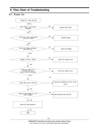
9. Flow Chart of Troubleshooting
This Document can not be used without Samsung's authorization
9-1
9-1. Power On
' Power On ' does not work
Yes
Yes
No
Download again
Check the Voltage of Battery
more than 3.3V
No
Check the Battery
Yes
Check the related circuit
No
Voltage of C302 = VBAT?
Yes
No
Check the VCCD_1.8V,
VCCD_2.9V and
VCCD_1.2V_A of UCP200
Yes
Check VRF_2.9V of RFT100
No
Check the UCD300 and C313, C100,
C103
Yes
Yes
Yes
Check OSC100 and RFT100
No
Check CLK26M_DBB on C113
Freq = 26MHz
Check the initial operation
END
Check the related circuit
Check the current consumption
more than 100mA
KEY FPCB or KEY Dome
damaged?
Replace Key FPCB
Yes
No
6. SAMSUNG Proprietary-Contents may change without notice
This Document can not be used without Samsung's authorization
Flow Chart of Troubleshooting
9-6
9-2. Initial
Initial Failure
Yes
RST = "H"?
(check the R230)
No
Check the circuit related to reset
Yes
END
9. SAMSUNG Proprietary-Contents may change without notice
Flow Chart of Troubleshooting
This Document can not be used without Samsung's authorization
9-9
9-3. Charging Part
Yes
Replace R301, R329
Check the circuit related
Check the circuit related to
VBUS_OUT_5V
Yes
NoCheck the R301 = 3.6Kohm?
& R329 = 4.3Kohm?
Yes
NoCheck the U300 pin 4.
under 0.4V?
Yes
No
END
Abnormal charging part
Check the Voltage Of L300.
under 5.0V?
Replace U300
11. SAMSUNG Proprietary-Contents may change without notice
Flow Chart of Troubleshooting
This Document can not be used without Samsung's authorization
9-11
C300
103C403C
103Q
R301
R329
033R
133R
003U
C224 L202
R235
R236
102AT
302U
12. SAMSUNG Proprietary-Contents may change without notice
This Document can not be used without Samsung's authorization
Flow Chart of Troubleshooting
9-12
9-4. Sim Part
Phone can't access SIM Card
Yes
Check the VSIM_2.9V of HDC501
2.9V ?
No
Check the circuit related
Yes
Check the SIM Card connector
No
Yes
END
Check the circuit around HDC501
input circuitry
14. SAMSUNG Proprietary-Contents may change without notice
This Document can not be used without Samsung's authorization
Flow Chart of Troubleshooting
9-14
9-5. Microphone Part
Microphone does not work
Yes
Resolder MIC
Check the connection
from MIC
No
Yes
Check the path from Main IC to MIC
Check the circuit
from UCD300 to MIC
No
Yes
Replace the MICCheck the MIC
No
Yes
END
On booting,
VAMICREF≒ 2.5V ?
Yes
No
Check UCD300
15. SAMSUNG Proprietary-Contents may change without notice
Flow Chart of Troubleshooting
This Document can not be used without Samsung's authorization
9-15
R404
C412
L402
C413
C411
GND1
2
GND
GND2
3 GND
OUT
4 OUT
POWER
1
POWER
MIC400
ZD400
MONO1_IN_P
VAMICREF
004CIM
16. SAMSUNG Proprietary-Contents may change without notice
This Document can not be used without Samsung's authorization
Flow Chart of Troubleshooting
9-16
9-6. Speaker Part(Melody)
Speaker does not work
Is the terminal of speaker
OK? check the speaker
No
Yes
No
check SPK_P (L400)
SPK_N (L401)
Check the
SPK_P & SPK_N
"HIGH"
Yes
Yes
Change speaker
Is it works?
END
No
No
Yes
Check HI_MONO_OUT_P,N
LO_MONO_OUT_P,N check the element related
Resolder of replace U400
18. SAMSUNG Proprietary-Contents may change without notice
This Document can not be used without Samsung's authorization
Flow Chart of Troubleshooting
9-18
9-7. Key Data Input
Check Initial Operation
Yes
When the END
keys is
pushed, is it
displayed on
Check Key PBA ass"y
& Key Pad
No
Yes
the circuit around
U500
input circuitry
Replace U500
No
Yes
END
Is it a QWERTY
key?
No
When one of the
keys is
pushed, is it
displayed on LCD?
Check the key Fpcb and
QWERTY Dome sheet
No
Yes
Yes
Check
HDC500
Is it
Replace the HDC500
No
Yes
END
Check
VCCD_2.9V=2.9V?
VCCD_1.9V=1.9V?
Check the
QWERTY Dome
sheet & Key Pad
No
Yes
21. SAMSUNG Proprietary-Contents may change without notice
Flow Chart of Troubleshooting
This Document can not be used without Samsung's authorization
9-21
9-8. Camera part
"Camera" function does not work
Yes
Is the Camera connected
on PBA?
Reconnect the camera module
No
Yes
CAM_2.8V_A = 2.8V?
CAM_2.8V = 2.8V?
CAM_1.5V=1.5?
Yes
END
Check the circuit related
No
Replace the Camera
22. SAMSUNG Proprietary-Contents may change without notice
This Document can not be used without Samsung's authorization
Flow Chart of Troubleshooting
9-22
R606
SHORT
R607
C607
CAM_1.5V
R608
SHORT
C613
CAM_2.8V_A
6 6
77 88
9 9
NC
22 23
NC
18 18
1919
2 2
2020
21 21
33 44
5 5
10 10
1111 1212
13 13 14 14
1515 1616
17 17
HDC601
1 1
R605
CAM_2.8V
C608
CAM_RST
CAM_HSYNC
CAM_D(1)
CAM_VSYNC
CAM_MCLK
CAM_D(2)
CAM_D(6)
CAM_D(4)
CAM_D(3)
CAM_D(5)
CAM_D(7)
CAM_D(0)
CAM_PCLK
CAM_SDA_2.8
CAM_SCL_2.8
706C
806C
016C
C611
C612
C614
HDC601
006L
506R
606R
806R
906R
106U
23. SAMSUNG Proprietary-Contents may change without notice
Flow Chart of Troubleshooting
This Document can not be used without Samsung's authorization
9-23
9-9. Radio part
Radio does not work
Yes
Resolder C422
check VCCD_1.9V on C422
Is it 1.9V?
Yes
check VCCD_2.9V on C423
Is it 2.9V?
No
Resolder C423
Yes
END
Resolder the U401
24. SAMSUNG Proprietary-Contents may change without notice
This Document can not be used without Samsung's authorization
Flow Chart of Troubleshooting
9-24
C415
614C
714C
224C
C423
005RAE
L403
804R704R
904R
014R
214R
104U
R410
13ROUT
RST
5
7
KLCS
OIDS
8
6
SEN VDD
11
10
OIV
17
14LOUT
LPI
4
NC
1
CN
2022
CN
CN
23
KLCR
9
3 RFGND
DFS
16
DOUT
15
FMI
2
12GND
21
DNG
19
1OPG
18
TNI_|2OPG
KLCD|3OPG
VCCD_2.9V
U401
VCCD_1.9V
R412
R409C415
C422
L403
R408
C417
C416
C423
R407
PCM_SYNC
PCM_RXDFM_ANT
PCM_CLK
FM_SDA_1.8
RTC_CLK
FM_BUS_EN
FM_INT
FM_SCL_1.8
RADIO_L
RADIO_R
25. SAMSUNG Proprietary-Contents may change without notice
Flow Chart of Troubleshooting
This Document can not be used without Samsung's authorization
9-25
PAM100 CHECK
pin17 ≥ -65dBm ?
9-10. GSM850 RX
CONTINUOUS RX ON
RF INPUT : 190CH
AMP : -50dBm
NORMAL CONDITION
catch the channel?
CHECK soldered
ANT contact
L101,C107,C108,L121,L100,C106,C112,C136
RFT100
pin 31 : 2.9V ?
PAM100 CHECK
pin11 ≥ -65dBm ?
RFT100 CHECK
pin24,25 ≥ -65dBm ?
PAM100, RFS100
resolder or change
PAM100
resolder or change
RFT100
resolder or change
UCD300 pin F3, C313,C314
change or resolder
RFT100 CHECK
pin 9,10
freq :26MHz ?
Vp-p : 380mV?
OSC100
change or resolder
RFT100
resolder or change
RFT100
pin 1,2,3,4 Vp-p
: 120mV ?
NO
YES
NO
NO
NO
NO
NO
NO
YES
YES
YES
YES
YES
YES
F100 CHECK
pin7,6 ≥ -65dBm ?
F100
resolder or change
YES
NO
GSM Receiver is O.K?
NO GSM RX path component
resolder or change
YES
END
26. SAMSUNG Proprietary-Contents may change without notice
This Document can not be used without Samsung's authorization
Flow Chart of Troubleshooting
9-26
PAM100 CHECK
pin17 ≥ -65dBm ?
9-11. EGSM RX
CONTINUOUS RX ON
RF INPUT : 62CH
AMP : -50dBm
NORMAL CONDITION
catch the channel?
CHECK soldered
ANT contact
L101,C107,C108,L121,L100,C106,C112,C136
RFT100
pin 31 : 2.9V ?
PAM100 CHECK
pin12 ≥ -65dBm ?
RFT100 CHECK
pin22,23 ≥ -65dBm ?
PAM100,RFS100
resolder or change
PAM100
resolder or change
RFT100
resolder or change
UCD300 pin F3, C313,C314
change or resolder
RFT100 CHECK
pin 9,10
freq :26MHz ?
Vp-p : 380mV?
OSC100
change or resolder
RFT100
resolder or change
RFT100
pin 1,2,3,4 Vp-p
: 120mV ?
NO
YES
NO
NO
NO
NO
NO
NO
YES
YES
YES
YES
YES
YES
F100 CHECK
pin9,8 ≥ -65dBm ?
F100
resolder or change
YES
NO
GSM Receiver is O.K?
NO GSM RX path component
resolder or change
YES
END
27. SAMSUNG Proprietary-Contents may change without notice
This Document can not be used without Samsung's authorization
Flow Chart of Troubleshooting
9-27
PAM100 CHECK
pin17 ≥ -65dBm ?
9-12. DCS RX
CONTINUOUS RX ON
RF INPUT : 698CH
AMP : -50dBm
YES
NORMAL CONDITION
catch the channel?
CHECK soldered
ANT contact
L101,C107,C108,L121,L100,C106,C112,C136
RFT100
pin 31 : 2.9V ?
PAM100 CHECK
pin13 ≥ -65dBm ?
RFT100 CHECK
pin19,20 ≥ -65dBm ?
PAM100,RFS100
resolder or change
PAM100
resolder or change
RFT100
resolder or change
UCD300 pin F3, C313,C314
change or resolder
RFT100 CHECK
pin 9,10
freq :26MHz ?
Vp-p : 380mV?
OSC100
change or resolder
RFT100
resolder or change
RFT100
pin 1,2,3,4 Vp-p
: 120mV ?
NO
YES
NO
NO
NO
NO
NO
YES
YES
YES
YES
YES
F101 CHECK
pin7,6 ≥ -65dBm ?
F101
resolder or change
YES
NO
NO
DCS Receiver is O.K?
YES
END
NO DCS RX path component
resolder or change
28. SAMSUNG Proprietary-Contents may change without notice
This Document can not be used without Samsung's authorization
Flow Chart of Troubleshooting
9-28
PAM100 CHECK
pin17 ≥ -65dBm ?
9-13. PCS RX
CONTINUOUS RX ON
RF INPUT : 661CH
AMP : -50dBm
YES
NORMAL CONDITION
catch the channel?
CHECK soldered
ANT contact
L101,C107,C108,L121,L100,C106,C112,C136
RFT100
pin 31 : 2.9V ?
PAM100 CHECK
pin14 ≥ -65dBm ?
RFT100 CHECK
pin17,18 ≥ -65dBm ?
PAM100,RFS100
resolder or change
PAM100
resolder or change
RFT100
resolder or change
UCD300 pin F3, C313,C314
change or resolder
RFT100 CHECK
pin 9,10
freq :26MHz ?
Vp-p : 380mV?
OSC100
change or resolder
RFT100
resolder or change
RFT100
pin 1,2,3,4 Vp-p
: 120mV ?
NO
YES
NO
NO
NO
NO
NO
YES
YES
YES
YES
YES
F101 CHECK
pin9,8 ≥ -65dBm ?
F101
resolder or change
YES
NO
NO
PCS Receiver is O.K?
YES
END
NO PCS RX path component
resolder or change
29. SAMSUNG Proprietary-Contents may change without notice
This Document can not be used without Samsung's authorization
Flow Chart of Troubleshooting
9-29
9-14. GSM850 TX
PAM100 pin17 :
about 2~3 dBm?
RFS100,L101,C107,
C108,L121,L100,C106,
C112,C136
check&change
PAM100
pin4 : 2.8 V?
UCD300
check & change
PAM100
pin30 : 3.7 V?
NO NO
YES
YES
NO BATTERY ,UCD300
check & change
PAM100
pin 3 : 1.2V ?
YES
NO
PAM100 pin17
about : -5dBm ?
YES
PAM100
pin 4 : 2.8V?
YES
YES
PAM100
change or resolder
NO
UCP200
check
Check R104
NO
RFT100
pin31 : 2.9V ?
UCD300
pinF3,C313,C314
change oresolder
YES
RFT100
pin9,10 : 26MHz ?
Vp-p : 380mV?
RFT100
pin1,2,3,4
:100mV?
YES
UCD300
change or resolder
NO
NO
RFT100
change or resolder
YES
NO
OSC100
change or resolder
CONTINOUS TX ON CONDITION
TX POWER DAC: 600 CODE APPLIED
CH : 190
RBW : 100KHz
VBW : 100KHz
SPAN : 10MHz
REF LEV. : 10dBm
ATT. : 20dB
30. SAMSUNG Proprietary-Contents may change without notice
This Document can not be used without Samsung's authorization
Flow Chart of Troubleshooting
9-30
9-15 EGSM TX
PAM100 pin17 :
about 2~3 dBm?
RFS100,L101,C107,
C108,L121,L100,C106,
C112,C136
check&change
PAM100
pin4 : 2.8 V?
UCD300
check & change
PAM100
pin30 : 3.7 V?
NO NO
YES
YES
NO BATTERY ,UCD300
check & change
PAM100
pin 3 : 1.2V ?
YES
NO
PAM100 pin17
about : -5dBm ?
YES
PAM100
pin 4 : 2.8V?
YES
YES
PAM100
change or resolder
NO
UCP200
check
Check R104
NO
RFT100
pin31 : 2.9V ?
UCD300
pinF3,C313,C314
change oresolder
YES
RFT100
pin9,10 : 26MHz ?
Vp-p : 380mV?
YES
UCD300
change or resolder
NO
NO
RFT100
change or resolder
YES
CONTINOUS TX ON CONDITION
TX POWER DAC: 600 CODE APPLIED
CH : 62
RBW : 100KHz
VBW : 100KHz
SPAN : 10MHz
REF LEV. : 10dBm
ATT. : 20dB
RFT100
pin1,2,3,4
:100mV?
NO
OSC100
change or resolder
31. SAMSUNG Proprietary-Contents may change without notice
This Document can not be used without Samsung's authorization
Flow Chart of Troubleshooting
9-31
9-16. DCS TX
PAM100 pin17 :
about 2~3 dBm?
RFS100,L101,C107,
C108,L121,L100,C106,
C112,C136
check&change
PAM100
pin4 : 2.8 V?
UCD300
check & change
PAM100
pin30 : 3.7 V?
NO NO
YES
YES
NO BATTERY ,UCD300
check & change
PAM100
pin 3 : 1.2V ?
YES
NO
PAM100 pin17
about : -5dBm ?
YES
PAM100
pin 4 : 2.8V?
YES
YES
PAM100
change or resolder
NO
UCP200
check
Check R104
NO
RFT100
pin31 : 2.9V ?
UCD300
pinF3,C313,C314
change oresolder
YES
RFT100
pin9,10 : 26MHz ?
Vp-p : 380mV?
YES
UCD300
change or resolder
NO
NO
RFT100
change or resolder
YES
CONTINOUS TX ON CONDITION
TX POWER DAC:520 CODE APPLIED
CH : 698
RBW : 100KHz
VBW : 100KHz
SPAN : 10MHz
REF LEV. : 10dBm
ATT. : 20dB
RFT100
pin1,2,3,4
:100mV?
NO
OSC100
change or resolder
32. SAMSUNG Proprietary-Contents may change without notice
This Document can not be used without Samsung's authorization
Flow Chart of Troubleshooting
9-32
9-17. PCS TX
PAM100 pin17 :
about 2~3 dBm?
RFS100,L101,C107,
C108,L121,L100,C106,
C112,C136
check&change
PAM100
pin4 : 2.8 V?
UCD300
check & change
PAM100
pin30 : 3.7 V?
NO NO
YES
YES
NO BATTERY ,UCD300
check & change
PAM100
pin 3 : 1.2V ?
YES
NO
PAM100 pin17
about : -5dBm ?
YES
PAM100
pin 4 : 2.8V?
YES
YES
PAM100
change or resolder
NO
UCP200
check
Check R104
NO
RFT100
pin31 : 2.9V ?
UCD300
pinF3,C313,C314
change oresolder
YES
RFT100
pin9,10 : 26MHz
?
Vp-p : 380mV?
YES
UCD300
change or resolder
NO
NO
RFT100
change or resolder
YES
CONTINOUS TX ON CONDITION
TX POWER DAC: 520 CODE APPLIED
CH : 661
RBW : 100KHz
VBW : 100KHz
SPAN : 10MHz
REF LEV. : 10dBm
ATT. : 20dB
RFT100
pin1,2,3,4
:100mV?
NO
OSC100
change or resolder
33. SAMSUNG Proprietary-Contents may change without notice
This Document can not be used without Samsung's authorization
Flow Chart of Troubleshooting
9-33
C111
C110
C100
R100
C113
VRF_2.9V
VRF_1.5V
C101
C105
C103
2
34
1
OSC100
VDD1
5
FSYS3
6
FSYS2
7
VDD2
8
XO
9
B
3
FERR
03
6DDV
13
DNG
23
DNG
33
CN
43
CN
53
BX
4
21
RX2
22
23
RX2X
RX1
24
25
RX1X
VDD4
26
2XT
72
1XT
82
5DDV
92
AD
51
NE
61
RX4
17
18
RX4X
RX3
19
AX
2
RX3X
20
GND
A
1
XOX
10
DNG
11
1SYSF
21
3DDV
31
KLC
41
RFT100
C104
C116
VRF_1.5VVRF_2.9V
C102
SBCK
SBDT
SBST
BT_CLK
DPCS_TX_IN
GSM850_RX_N
GSM900_RX_N
GSM900_RX_P
DCS_RX_N
RTX_I_N
PCS_RX_N
RTX_I_P
GSM_TX_IN
CLK26M_DBB
PCS_RX_P
GSM850_RX_P
DCS_RX_P
RTX_Q_N
RTX_Q_P
VBAT
L114
C120 C121
C107
L105
12
13RX3
RX4 14
TX_EN
4
03TTABV
VLOGIC
2
3
VRAMP
G
G
01
51
G
G
61
G
81
G
91
27
GSM_IN
11RX1
RX2
G
G
23
7
G
33
G
G
43
G
53
G
63
G
8
9
02
12
G
G
22
32
G
G
42
G
52
G
62
G
82
13
71TNA
5BS1
BS2 6
DCS|PCS_IN
29
1
G
G
C112
PAM100
2
1
L121
G G
3
G
510
G
CDMA_OUT 6
7CDMA_OUT
CDMA_IN4
1 EGSM_IN EGSM_OUT 8
9EGSM_OUT
2
L107
F100
L104
C123
C114
2
C1
G3
G
4
RFS100
A
L102
C108
L115
L108
L106
L110
C115
C136
C119
R104
C122
L112 1 GSM1900_IN 8GSM1900_OUT
GSM1900_OUT 9
2G
G3
G5
01G
4 GSM1800_IN 6GSM1800_OUT
GSM1800_OUT 7
F101
L103
L111
C118
L113
C124
L101
1 2
L100
SGHG770-ANT
ANT100
C106
VR100
NC
L109
PCS_RX_P
BAND_SEL2
BAND_SEL1
DPCS_TX_IN
PAM_VLOGIC
GSM_TX_IN
PAM_ON
PAM_VRAMP
GSM850_RX_P
GSM850_RX_N
GSM900_RX_N
GSM900_RX_P
DCS_RX_N
DCS_RX_P
PCS_RX_N
35. SAMSUNG Proprietary-Contents may change without notice
This Document can not be used without Samsung's authorization
Flow Chart of Troubleshooting
9-35
9-14. Bluetooth part
Bluetooth connection disable
Yes
Check BT function ON Enable BT function
No
Yes
Check power of U100,
VBT_1.8V ≒ 1.8V,
VBT_1.5V ≒ 1.5V?
No
Resolder U100
Check pin A3 of U100
(26MHz)
Yes
Resolder C110
No
Yes
Check the assembled
status of
F102,C137,C138,L120,L116,
C133,L118
No
Resolder error parts
Yes
Check the assembled status
of ANT101
No
Resolder ANT101
Yes
END
37. SAMSUNG Proprietary-Contents may change without notice
This Document can not be used without Samsung's authorization
Flow Chart of Troubleshooting
9-37
C125
C126
C127
C128
C129
C130
C133
C134
C137 201F
611L
L118
R105
R106
R107
R315
206R
DXR_TB_PT
TP_BT_TXD
U100
38. SAMSUNG Proprietary-Contents may change without notice
7. Block Diagrams
7-1
This Document can not be used without Samsung's authorization
RF Block
39. SAMSUNG Proprietary-Contents may change without notice
Block Diagrams
7-2
This Document can not be used without Samsung's authorization
Bluetooth Block
40. SAMSUNG Proprietary-Contents may change without notice
Block Diagrams
7-3
This Document can not be used without Samsung's authorization
Audio Block (+ FM radio)
41. SAMSUNG Proprietary-Contents may change without notice
Block Diagrams
7-4
This Document can not be used without Samsung's authorization
Display (LCD) Block
42. SAMSUNG Proprietary-Contents may change without notice
Block Diagrams
7-5
This Document can not be used without Samsung's authorization
Camera Block