Download to read offline

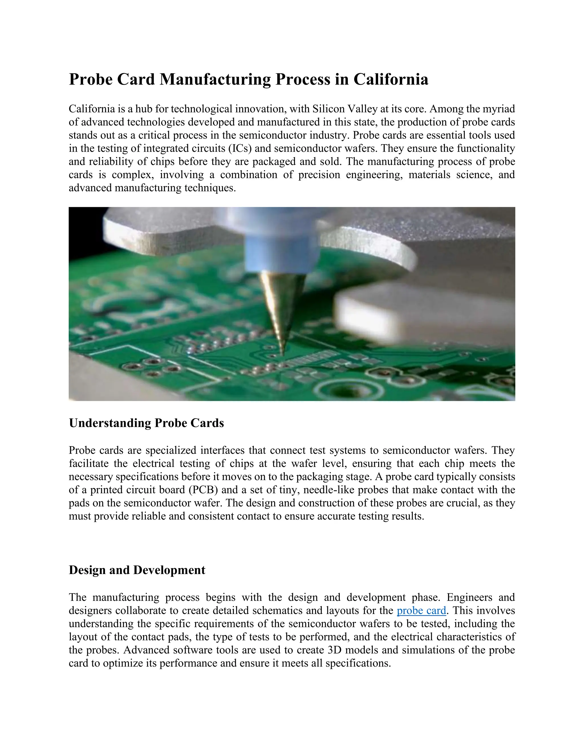

California is a hub for the manufacturing of probe cards, essential tools in testing integrated circuits and semiconductor wafers. The manufacturing process involves detailed design, material selection, precision fabrication, assembly, and rigorous quality control to ensure reliability and performance. The industry is continually evolving, focusing on innovation, sustainability, and addressing challenges due to advancements in semiconductor technology.


