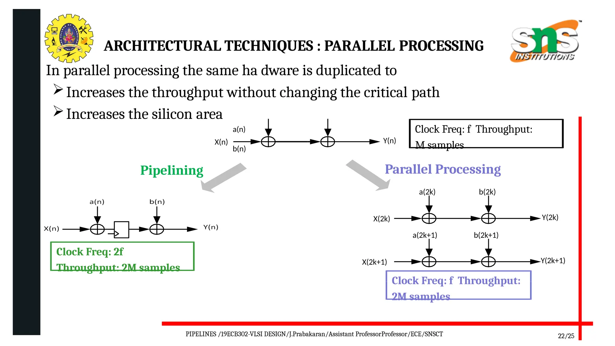
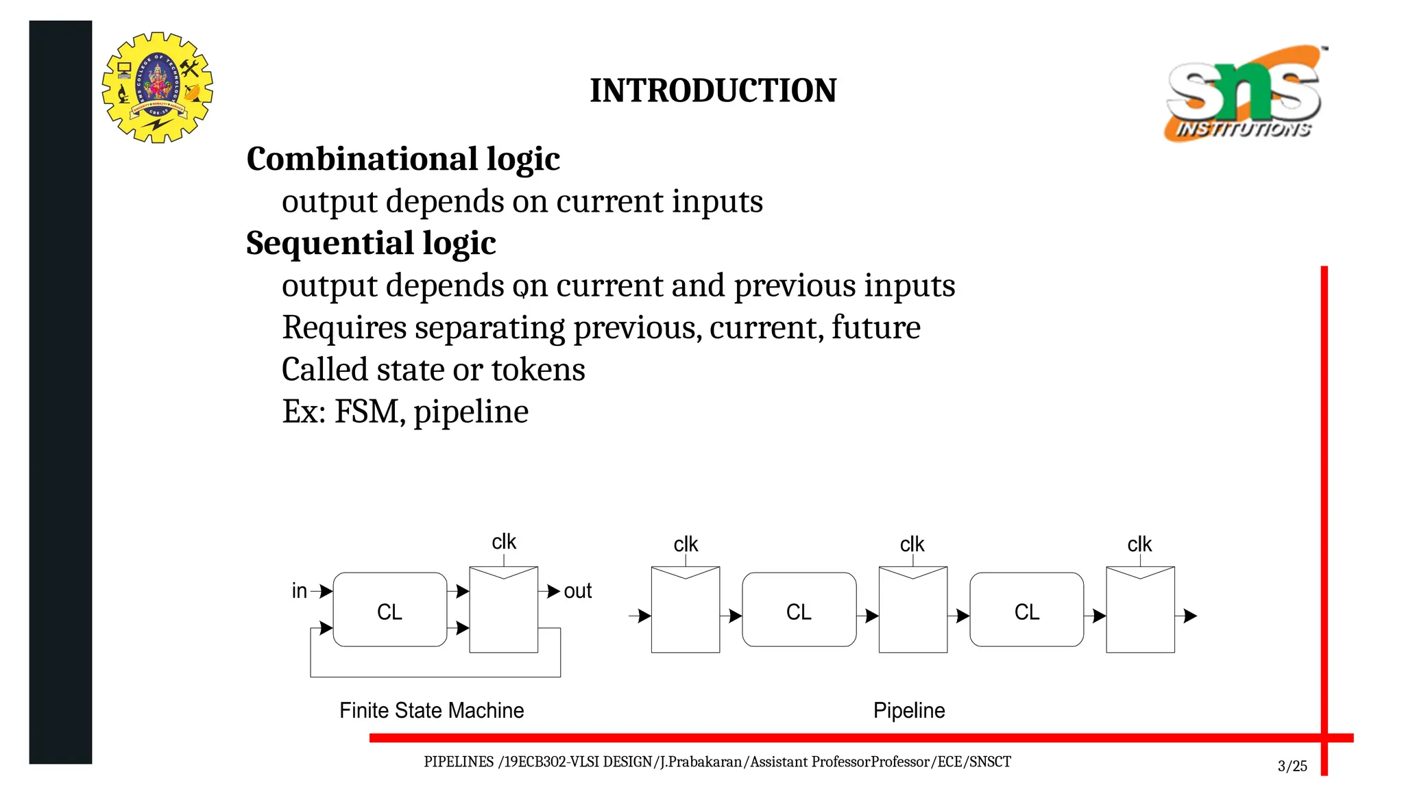
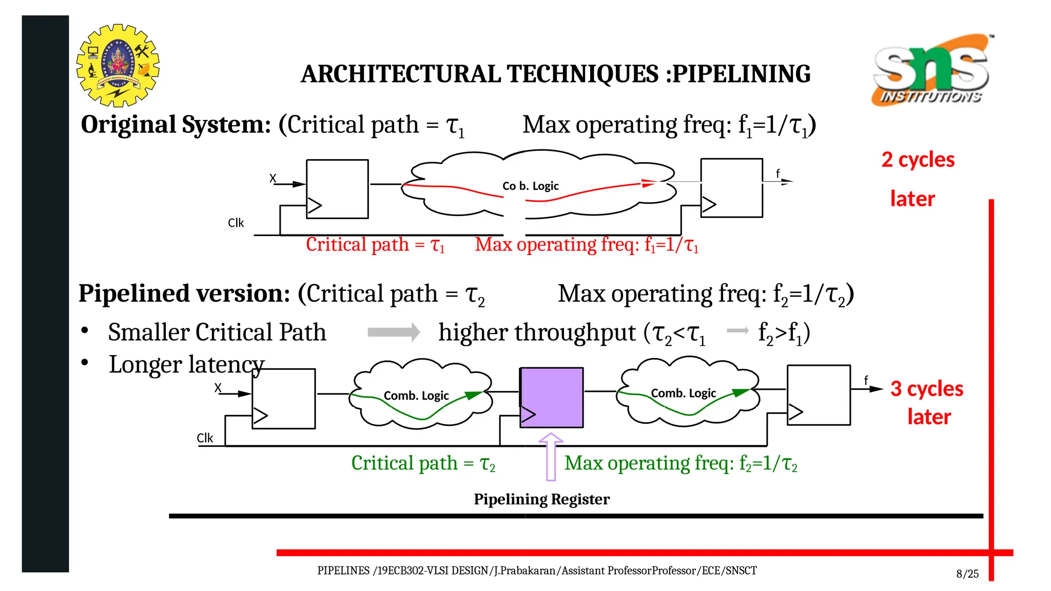
09/10/2025
SNS COLLEGE OF TECHNOLOGY
Coimbatore-35
An Autonomous Institution
Accredited by NBA – AICTE and Accredited by NAAC – UGC with ‘A+’ Grade
Approved by AICTE, New Delhi & Affiliated to Anna University, Chennai
DEPARTMENT OF ELECTRONICS & COMMUNICATION ENGINEERING
19ECB302–VLSI DESIGN
III YEAR/ V SEMESTER
UNIT 3 –SEQUENTIAL LOGIC CIRCUITS
TOPIC 4 –PIPELINES
PIPELINES /19ECB302-VLSI DESIGN/J.Prabakaran/Assistant ProfessorProfessor/ECE/SNSCT
OUTLINE
• Introduction
• Architectural techniques : critical path
• Synchronous timing
• Self-timed pipelined data path
• Completion signal using current sensing
• Architectural techniques :pipelining
• Activity
• Architectural techniques : fine grain pipelining
‐
• Unrolling the loop using pipelining
• Architectural techniques : parallel processing
• Assessment
• Summary & thank you
PIPELINES /19ECB302-VLSI DESIGN/J.Prabakaran/Assistant ProfessorProfessor/ECE/SNSCT 2/25
INTRODUCTION
3/25
Y
CL
clk
in out
clk clk clk
CL CL
Pipeline
Finite State Machine
Combinational logic
output depends on current inputs
Sequential logic
output depends on current and previous inputs
Requires separating previous, current, future
Called state or tokens
Ex: FSM, pipeline
PIPELINES /19ECB302-VLSI DESIGN/J.Prabakaran/Assistant ProfessorProfessor/ECE/SNSCT
4/25
Y
ARCHITECTURAL TECHNIQUES : CRITICAL PATH
Critical path in any design is the longest path between
1. Any two internal latches/flip flops
‐
2. An input pad and an internal latch
3. An internal latch and an output pad
4. An input pad and an output pad
•Use FFs right after/before
input/out pads to avoid the last
three cases (off chip and
‐
packaging delay)
PIPELINES /19ECB302-VLSI DESIGN/J.Prabakaran/Assistant ProfessorProfessor/ECE/SNSCT
SYNCHRONOUS TIMING
5/25
Y
In
tpd,reg tpd1
D
R1
Q
CLK
Logic
Block #1
tpd2
D
R2
Q
Logic
Block #2
tpd3
D
R3
Q D
R4
Q
Pipelining:
• Comes from the idea of a water pipe: continue sending water
without waiting the water in the pipe tbe out
• Used to reduce the critical path of the design
PIPELINES /19ECB302-VLSI DESIGN/J.Prabakaran/Assistant ProfessorProfessor/ECE/SNSCT
09/10/2025
SELF-TIMED PIPELINED DATA PATH
6/25
23/06/2020
R2 Out
F2
In
tpF2
Start Done
R1 F1
tpF1
Start Done
R3 F3
tpF3
Start Done
Req Req Req Req
Ack Ack Ack ACK
HS HS HS
PIPELINES /19ECB302-VLSI DESIGN/J.Prabakaran/Assistant ProfessorProfessor/ECE/SNSCT
COMPLETION SIGNAL USING CURRENT SENSING
7/25
Min Delay Generator
Start
GNDsense
VDD
Inputs
Current Sensor
Static CMOS Logic
In
p
u
t
R
e
g
iste
r
Done
Output
A
B
tdelay
toverlap
tpd-NOR
tMDG
Start
A
B
Done
Output valid
PIPELINES /19ECB302-VLSI DESIGN/J.Prabakaran/Assistant ProfessorProfessor/ECE/SNSCT
ARCHITECTURAL TECHNIQUES :PIPELINING
X
• Smaller Critical Path
• Longer latency
Comb. Logic
X
Clk
• Original System: (Critical path = τ1 Max operating freq: f1=1/τ1)
2 cycles
f
later
Co b. Logic
Clk
Critical path = τ1 Max operating freq: f1=1/τ1
• Pipelined version: (Critical path = τ2 Max operating freq: f2=1/τ2)
higher throughput (τ2<τ1 f2>f1)
Comb. Logic
f
3 cycles
later
Critical path = τ2 Max operating freq: f2=1/τ2
Pipelining Register
8/25
PIPELINES /19ECB302-VLSI DESIGN/J.Prabakaran/Assistant ProfessorProfessor/ECE/SNSCT
ARCHITECTURAL TECHNIQUES : PIPELINE DEPTH
Pipeline depth: 0 (No Pipeline)
Critical path: 3 Adders
t1 t2
wire w1, w2;
assign w1 = X + a;
assign w2 = w1 + b;
assign Y = w2 + c;
time
t3
X(2)
X(1) X(3)
Y(1) Y(2) Y(3)
9/25
PIPELINES /19ECB302-VLSI DESIGN/J.Prabakaran/Assistant ProfessorProfessor/ECE/SNSCT
ARCHITECTURAL TECHNIQUES : PIPELINE DEPTH
• Pipeline depth: 1 (One Pipeline register Added)
• Critical path: 2 Adders
a(n) b(n)
X(n)
w1 w2
t1 t2
wire w1;
reg w2;
assign w1 = X + a;
assign Y = w2 + c;
c(n)
always @(posedge Clk)
w2 <= w1 + b;
Y(n)
time
t3 t4
Y(3)
X(1) X(2) X(3)
Y(1) Y(2)
10/25
PIPELINES /19ECB302-VLSI DESIGN/J.Prabakaran/Assistant ProfessorProfessor/ECE/SNSCT
ARCHITECTURAL TECHNIQUES : PIPELINE DEPTH
t1 t2 t3
X(1) X(2)
• Pipeline depth: 2 (One Pipeline register Added)
• Critical path: 1 Adder reg w1, w2; assign
Y = w2 + c;
always @(posedge Clk)
begin
w1 <= X + a;
w2 <= w1 + b;
end
t4 t5
Y(1) Y(2)
X(3)
Y(3)
11/25
PIPELINES /19ECB302-VLSI DESIGN/J.Prabakaran/Assistant ProfessorProfessor/ECE/SNSCT
ARCHITECTURAL TECHNIQUES :PIPELINING
• Clock period and throughput as a function of pipeline depth:
• Clock period :
n

1
Clk

• Throughput: T  n
Adding register layers improves
timing by dividing the critical path
into two paths of smaller delay
Clock Period
Throughput
3 5 6
4
Pipeline Depth
12/25
PIPELINES /19ECB302-VLSI DESIGN/J.Prabakaran/Assistant ProfessorProfessor/ECE/SNSCT
Architectural Techniques : Pipelining
General Rule:
 Pipelining latches can only be placed across feed forward
‐ cutsets
of the circuit.
Cut set:
A set of paths of a circuit such that if these paths are removed, the
circuit becomes disjoint (i.e., two separate pieces)
Feed Forward
‐ Cutset:
A cutset is called feed forward
‐ cutset if the data move in the
forward direction on all the paths of the cutset
13/25
PIPELINES /19ECB302-VLSI DESIGN/J.Prabakaran/Assistant ProfessorProfessor/ECE/SNSCT
ARCHITECTURAL TECHNIQUES : PIPELINING
• Example:
• FIR Filter
• Three feed forward
‐ cutsets ar NOT a feed forward
‐ cutset
X(n) X(n 1)
‐ X(n 2)
‐
a b c
Y(n)
14/25
PIPELINES /19ECB302-VLSI DESIGN/J.Prabakaran/Assistant ProfessorProfessor/ECE/SNSCT
CLASS ROOM ACTIVITY
23/06/2020 15/25
Group Discussion & Debate
PIPELINES /19ECB302-VLSI DESIGN/J.Prabakaran/Assistant ProfessorProfessor/ECE/SNSCT
ARCHITECTURAL TECHNIQUES : PIPELINING
Critical Path: 1M+2A Critical Path: 2A
X(n) X(n‐1) X(n 2)
‐
a b c
Y(n)
w1 w2
w3
w4
assign w1 = a*Xn; assign
w2 = b*Xn_1 ; assign w3
= w1 + w2; assign w4 =
c*Xn_2; assign Y = w3 +
w4; always @(posedge
Clk) begin
Xn_1 <= Xn;
Xn_2 <= Xn_1;
end
assign Y = r3 + w1; assign
w1 = r1 + r2; always
@(posedge Clk) begin
Xn_1 <= Xn;
Xn_2 <= Xn_1; r1
<= a*Xn;
r2 <= b*Xn_1; r3
<= c*Xn_2;
end
16/25
PIPELINES /19ECB302-VLSI DESIGN/J.Prabakaran/Assistant ProfessorProfessor/ECE/SNSCT
ARCHITECTURAL TECHNIQUES : PIPELINING
X(n) X(n 1)
‐
a b
2
1 3
X(n‐2)
c
4
Y(n)
5
Cloc k Input 1 2 3 4 5 Output
0 X(0) aX(0) ‐ aX(0) ‐ aX(0) Y(0)
1 X(1) aX(1) bX(0) aX(1)+bX(0) ‐ aX(1)+bX(0) Y(1)
2 X(2) aX(2) bX(1) aX(2)+bX(1) cX(0) aX(2)+bX(1)+cX(0) Y(2)
3 X(3) aX(3) bX(2) aX(3)+bX(2) cX(1) aX(3)+bX(2)+cX(1) Y(3)
17/25
PIPELINES /19ECB302-VLSI DESIGN/J.Prabakaran/Assistant ProfessorProfessor/ECE/SNSCT
ARCHITECTURAL TECHNIQUES : PIPELINING
Even more pipelining
Clock Input 1 2 3
0 X(0) ‐ ‐ ‐
1 X(1) aX(0) ‐ -
2 X(2) aX(1) bX(0) aX(0)
3 X(3) aX(2) bX(1) aX(1)+bX(0)
4 X(3) aX(2) bX(1) aX(2)+bX(1)
4 5 Output
‐ ‐ ‐
‐ - -
‐ aX(0) Y(0)
‐ aX(1)+bX(0) Y(1)
cX(0) aX(2)+bX(1)+cX(0) Y(2)
18/25
PIPELINES /19ECB302-VLSI DESIGN/J.Prabakaran/Assistant ProfessorProfessor/ECE/SNSCT
ARCHITECTURAL TECHNIQUES : FINE GRAIN
‐ PIPELINING
• Pipelining at the operation level
• Break the multiplier into two parts
X(n) X(n‐1) X(n 2)
‐
a b c
m1 m1 m1
Fine Grain
‐
m2 m2 m2
Pipelining
Y(n)
19/25
PIPELINES /19ECB302-VLSI DESIGN/J.Prabakaran/Assistant ProfessorProfessor/ECE/SNSCT
UNROLLING THE LOOP USING PIPELINING
• Calculation of X3
• Throughput = 8/3, or 2.7
bits/clock
module power3( output reg [7:0]
X3, output finished,
• Timing = One multiplier in the critical path
• Iterative implementation:
• No new computations can begin until the
previous computation has completed
input [7:0] X, input clk,
start); reg [7:0] ncount;
reg [7:0] Xpower, Xin;
assign finished = (ncount == 0);
always@(posedge clk)
if (start) begin XPower <= X;
Xin<=X; ncount <= 2;
X3 <= XPower; end
else if(!finished) begin ncount <=
ncount ‐ 1; XPower <=
XPower * Xin;
End
endmodule
20/25
PIPELINES /19ECB302-VLSI DESIGN/J.Prabakaran/Assistant ProfessorProfessor/ECE/SNSCT
REMOVING PIPELINE REGISTERS (TO IMPROVE LATENCY)
• Latency = 0 clocks
• Calculation of X3
• Throughput = 8 bits/clock (3X improvement)
Timing = Two multipliers in the critical
path
module
power3( Output [7:0]
XPower,
Latency can be reduced by removing pipeline registers
input [7:0] X);
reg [7:0] XPower1, XPower2; reg
[7:0] X1, X2;
always @*
XPower1 = X;
always @(*)
begin
X2 = XPower1;
XPower2 = XPower1*XPower1;
end
assign XPower = XPower2 * X2;
endmodule
21/25
PIPELINES /19ECB302-VLSI DESIGN/J.Prabakaran/Assistant ProfessorProfessor/ECE/SNSCT
ARCHITECTURAL TECHNIQUES : PARALLEL PROCESSING
X(n)
Pipelining
Clock Freq: 2f
Throughput: 2M samples
 In parallel processing the same ha dware is duplicated to
Increases the throughput without changing the critical path
Increases the silicon area
a(n)
b(n)
Y(n)
Clock Freq: f Throughput:
M samples
a(2k) b(2k)
Parallel Processing
X(2k) Y(2k)
a(2k+1) b(2k+1)
X(2k+1) Y(2k+1)
Clock Freq: f Throughput:
2M samples
22/25
PIPELINES /19ECB302-VLSI DESIGN/J.Prabakaran/Assistant ProfessorProfessor/ECE/SNSCT
09/10/2025 PIPELINES /19ECB302-VLSI DESIGN/J.Prabak
aran/Assistant ProfessorProfessor/ECE/SNS
CT
ADVANTAGEOUS
• Reduction in the critical path
• Higher throughput (number of computed results in a give time)
• Increases the clock speed (or sampling speed)
• Reduces the power consumption at same speed
23/06/2020 23/25
PIPELINES /19ECB302-VLSI DESIGN/J.Prabakaran/Assistant ProfessorProfessor/ECE/SNSCT
ASSESSMENT
24/25
• Define critical path
• List out the needs of Pipeline
• Draw the FIR filter using pipeline processing
• Compare pipeline and parallel processing
PIPELINES /19ECB302-VLSI DESIGN/J.Prabakaran/Assistant ProfessorProfessor/ECE/SNSCT
SUMMARY & THANK YOU
25/25
PIPELINES /19ECB302-VLSI DESIGN/J.Prabakaran/Assistant ProfessorProfessor/ECE/SNSCT

Pipelines CONCEPT in VLSI SYSTEM DESIGN.pptx

  • 1.
    09/10/2025 SNS COLLEGE OFTECHNOLOGY Coimbatore-35 An Autonomous Institution Accredited by NBA – AICTE and Accredited by NAAC – UGC with ‘A+’ Grade Approved by AICTE, New Delhi & Affiliated to Anna University, Chennai DEPARTMENT OF ELECTRONICS & COMMUNICATION ENGINEERING 19ECB302–VLSI DESIGN III YEAR/ V SEMESTER UNIT 3 –SEQUENTIAL LOGIC CIRCUITS TOPIC 4 –PIPELINES PIPELINES /19ECB302-VLSI DESIGN/J.Prabakaran/Assistant ProfessorProfessor/ECE/SNSCT
  • 2.
    OUTLINE • Introduction • Architecturaltechniques : critical path • Synchronous timing • Self-timed pipelined data path • Completion signal using current sensing • Architectural techniques :pipelining • Activity • Architectural techniques : fine grain pipelining ‐ • Unrolling the loop using pipelining • Architectural techniques : parallel processing • Assessment • Summary & thank you PIPELINES /19ECB302-VLSI DESIGN/J.Prabakaran/Assistant ProfessorProfessor/ECE/SNSCT 2/25
  • 3.
    INTRODUCTION 3/25 Y CL clk in out clk clkclk CL CL Pipeline Finite State Machine Combinational logic output depends on current inputs Sequential logic output depends on current and previous inputs Requires separating previous, current, future Called state or tokens Ex: FSM, pipeline PIPELINES /19ECB302-VLSI DESIGN/J.Prabakaran/Assistant ProfessorProfessor/ECE/SNSCT
  • 4.
    4/25 Y ARCHITECTURAL TECHNIQUES :CRITICAL PATH Critical path in any design is the longest path between 1. Any two internal latches/flip flops ‐ 2. An input pad and an internal latch 3. An internal latch and an output pad 4. An input pad and an output pad •Use FFs right after/before input/out pads to avoid the last three cases (off chip and ‐ packaging delay) PIPELINES /19ECB302-VLSI DESIGN/J.Prabakaran/Assistant ProfessorProfessor/ECE/SNSCT
  • 5.
    SYNCHRONOUS TIMING 5/25 Y In tpd,reg tpd1 D R1 Q CLK Logic Block#1 tpd2 D R2 Q Logic Block #2 tpd3 D R3 Q D R4 Q Pipelining: • Comes from the idea of a water pipe: continue sending water without waiting the water in the pipe tbe out • Used to reduce the critical path of the design PIPELINES /19ECB302-VLSI DESIGN/J.Prabakaran/Assistant ProfessorProfessor/ECE/SNSCT
  • 6.
    09/10/2025 SELF-TIMED PIPELINED DATAPATH 6/25 23/06/2020 R2 Out F2 In tpF2 Start Done R1 F1 tpF1 Start Done R3 F3 tpF3 Start Done Req Req Req Req Ack Ack Ack ACK HS HS HS PIPELINES /19ECB302-VLSI DESIGN/J.Prabakaran/Assistant ProfessorProfessor/ECE/SNSCT
  • 7.
    COMPLETION SIGNAL USINGCURRENT SENSING 7/25 Min Delay Generator Start GNDsense VDD Inputs Current Sensor Static CMOS Logic In p u t R e g iste r Done Output A B tdelay toverlap tpd-NOR tMDG Start A B Done Output valid PIPELINES /19ECB302-VLSI DESIGN/J.Prabakaran/Assistant ProfessorProfessor/ECE/SNSCT
  • 8.
    ARCHITECTURAL TECHNIQUES :PIPELINING X •Smaller Critical Path • Longer latency Comb. Logic X Clk • Original System: (Critical path = τ1 Max operating freq: f1=1/τ1) 2 cycles f later Co b. Logic Clk Critical path = τ1 Max operating freq: f1=1/τ1 • Pipelined version: (Critical path = τ2 Max operating freq: f2=1/τ2) higher throughput (τ2<τ1 f2>f1) Comb. Logic f 3 cycles later Critical path = τ2 Max operating freq: f2=1/τ2 Pipelining Register 8/25 PIPELINES /19ECB302-VLSI DESIGN/J.Prabakaran/Assistant ProfessorProfessor/ECE/SNSCT
  • 9.
    ARCHITECTURAL TECHNIQUES :PIPELINE DEPTH Pipeline depth: 0 (No Pipeline) Critical path: 3 Adders t1 t2 wire w1, w2; assign w1 = X + a; assign w2 = w1 + b; assign Y = w2 + c; time t3 X(2) X(1) X(3) Y(1) Y(2) Y(3) 9/25 PIPELINES /19ECB302-VLSI DESIGN/J.Prabakaran/Assistant ProfessorProfessor/ECE/SNSCT
  • 10.
    ARCHITECTURAL TECHNIQUES :PIPELINE DEPTH • Pipeline depth: 1 (One Pipeline register Added) • Critical path: 2 Adders a(n) b(n) X(n) w1 w2 t1 t2 wire w1; reg w2; assign w1 = X + a; assign Y = w2 + c; c(n) always @(posedge Clk) w2 <= w1 + b; Y(n) time t3 t4 Y(3) X(1) X(2) X(3) Y(1) Y(2) 10/25 PIPELINES /19ECB302-VLSI DESIGN/J.Prabakaran/Assistant ProfessorProfessor/ECE/SNSCT
  • 11.
    ARCHITECTURAL TECHNIQUES :PIPELINE DEPTH t1 t2 t3 X(1) X(2) • Pipeline depth: 2 (One Pipeline register Added) • Critical path: 1 Adder reg w1, w2; assign Y = w2 + c; always @(posedge Clk) begin w1 <= X + a; w2 <= w1 + b; end t4 t5 Y(1) Y(2) X(3) Y(3) 11/25 PIPELINES /19ECB302-VLSI DESIGN/J.Prabakaran/Assistant ProfessorProfessor/ECE/SNSCT
  • 12.
    ARCHITECTURAL TECHNIQUES :PIPELINING •Clock period and throughput as a function of pipeline depth: • Clock period : n  1 Clk  • Throughput: T  n Adding register layers improves timing by dividing the critical path into two paths of smaller delay Clock Period Throughput 3 5 6 4 Pipeline Depth 12/25 PIPELINES /19ECB302-VLSI DESIGN/J.Prabakaran/Assistant ProfessorProfessor/ECE/SNSCT
  • 13.
    Architectural Techniques :Pipelining General Rule:  Pipelining latches can only be placed across feed forward ‐ cutsets of the circuit. Cut set: A set of paths of a circuit such that if these paths are removed, the circuit becomes disjoint (i.e., two separate pieces) Feed Forward ‐ Cutset: A cutset is called feed forward ‐ cutset if the data move in the forward direction on all the paths of the cutset 13/25 PIPELINES /19ECB302-VLSI DESIGN/J.Prabakaran/Assistant ProfessorProfessor/ECE/SNSCT
  • 14.
    ARCHITECTURAL TECHNIQUES :PIPELINING • Example: • FIR Filter • Three feed forward ‐ cutsets ar NOT a feed forward ‐ cutset X(n) X(n 1) ‐ X(n 2) ‐ a b c Y(n) 14/25 PIPELINES /19ECB302-VLSI DESIGN/J.Prabakaran/Assistant ProfessorProfessor/ECE/SNSCT
  • 15.
    CLASS ROOM ACTIVITY 23/06/202015/25 Group Discussion & Debate PIPELINES /19ECB302-VLSI DESIGN/J.Prabakaran/Assistant ProfessorProfessor/ECE/SNSCT
  • 16.
    ARCHITECTURAL TECHNIQUES :PIPELINING Critical Path: 1M+2A Critical Path: 2A X(n) X(n‐1) X(n 2) ‐ a b c Y(n) w1 w2 w3 w4 assign w1 = a*Xn; assign w2 = b*Xn_1 ; assign w3 = w1 + w2; assign w4 = c*Xn_2; assign Y = w3 + w4; always @(posedge Clk) begin Xn_1 <= Xn; Xn_2 <= Xn_1; end assign Y = r3 + w1; assign w1 = r1 + r2; always @(posedge Clk) begin Xn_1 <= Xn; Xn_2 <= Xn_1; r1 <= a*Xn; r2 <= b*Xn_1; r3 <= c*Xn_2; end 16/25 PIPELINES /19ECB302-VLSI DESIGN/J.Prabakaran/Assistant ProfessorProfessor/ECE/SNSCT
  • 17.
    ARCHITECTURAL TECHNIQUES :PIPELINING X(n) X(n 1) ‐ a b 2 1 3 X(n‐2) c 4 Y(n) 5 Cloc k Input 1 2 3 4 5 Output 0 X(0) aX(0) ‐ aX(0) ‐ aX(0) Y(0) 1 X(1) aX(1) bX(0) aX(1)+bX(0) ‐ aX(1)+bX(0) Y(1) 2 X(2) aX(2) bX(1) aX(2)+bX(1) cX(0) aX(2)+bX(1)+cX(0) Y(2) 3 X(3) aX(3) bX(2) aX(3)+bX(2) cX(1) aX(3)+bX(2)+cX(1) Y(3) 17/25 PIPELINES /19ECB302-VLSI DESIGN/J.Prabakaran/Assistant ProfessorProfessor/ECE/SNSCT
  • 18.
    ARCHITECTURAL TECHNIQUES :PIPELINING Even more pipelining Clock Input 1 2 3 0 X(0) ‐ ‐ ‐ 1 X(1) aX(0) ‐ - 2 X(2) aX(1) bX(0) aX(0) 3 X(3) aX(2) bX(1) aX(1)+bX(0) 4 X(3) aX(2) bX(1) aX(2)+bX(1) 4 5 Output ‐ ‐ ‐ ‐ - - ‐ aX(0) Y(0) ‐ aX(1)+bX(0) Y(1) cX(0) aX(2)+bX(1)+cX(0) Y(2) 18/25 PIPELINES /19ECB302-VLSI DESIGN/J.Prabakaran/Assistant ProfessorProfessor/ECE/SNSCT
  • 19.
    ARCHITECTURAL TECHNIQUES :FINE GRAIN ‐ PIPELINING • Pipelining at the operation level • Break the multiplier into two parts X(n) X(n‐1) X(n 2) ‐ a b c m1 m1 m1 Fine Grain ‐ m2 m2 m2 Pipelining Y(n) 19/25 PIPELINES /19ECB302-VLSI DESIGN/J.Prabakaran/Assistant ProfessorProfessor/ECE/SNSCT
  • 20.
    UNROLLING THE LOOPUSING PIPELINING • Calculation of X3 • Throughput = 8/3, or 2.7 bits/clock module power3( output reg [7:0] X3, output finished, • Timing = One multiplier in the critical path • Iterative implementation: • No new computations can begin until the previous computation has completed input [7:0] X, input clk, start); reg [7:0] ncount; reg [7:0] Xpower, Xin; assign finished = (ncount == 0); always@(posedge clk) if (start) begin XPower <= X; Xin<=X; ncount <= 2; X3 <= XPower; end else if(!finished) begin ncount <= ncount ‐ 1; XPower <= XPower * Xin; End endmodule 20/25 PIPELINES /19ECB302-VLSI DESIGN/J.Prabakaran/Assistant ProfessorProfessor/ECE/SNSCT
  • 21.
    REMOVING PIPELINE REGISTERS(TO IMPROVE LATENCY) • Latency = 0 clocks • Calculation of X3 • Throughput = 8 bits/clock (3X improvement) Timing = Two multipliers in the critical path module power3( Output [7:0] XPower, Latency can be reduced by removing pipeline registers input [7:0] X); reg [7:0] XPower1, XPower2; reg [7:0] X1, X2; always @* XPower1 = X; always @(*) begin X2 = XPower1; XPower2 = XPower1*XPower1; end assign XPower = XPower2 * X2; endmodule 21/25 PIPELINES /19ECB302-VLSI DESIGN/J.Prabakaran/Assistant ProfessorProfessor/ECE/SNSCT
  • 22.
    ARCHITECTURAL TECHNIQUES :PARALLEL PROCESSING X(n) Pipelining Clock Freq: 2f Throughput: 2M samples  In parallel processing the same ha dware is duplicated to Increases the throughput without changing the critical path Increases the silicon area a(n) b(n) Y(n) Clock Freq: f Throughput: M samples a(2k) b(2k) Parallel Processing X(2k) Y(2k) a(2k+1) b(2k+1) X(2k+1) Y(2k+1) Clock Freq: f Throughput: 2M samples 22/25 PIPELINES /19ECB302-VLSI DESIGN/J.Prabakaran/Assistant ProfessorProfessor/ECE/SNSCT
  • 23.
    09/10/2025 PIPELINES /19ECB302-VLSIDESIGN/J.Prabak aran/Assistant ProfessorProfessor/ECE/SNS CT ADVANTAGEOUS • Reduction in the critical path • Higher throughput (number of computed results in a give time) • Increases the clock speed (or sampling speed) • Reduces the power consumption at same speed 23/06/2020 23/25 PIPELINES /19ECB302-VLSI DESIGN/J.Prabakaran/Assistant ProfessorProfessor/ECE/SNSCT
  • 24.
    ASSESSMENT 24/25 • Define criticalpath • List out the needs of Pipeline • Draw the FIR filter using pipeline processing • Compare pipeline and parallel processing PIPELINES /19ECB302-VLSI DESIGN/J.Prabakaran/Assistant ProfessorProfessor/ECE/SNSCT
  • 25.
    SUMMARY & THANKYOU 25/25 PIPELINES /19ECB302-VLSI DESIGN/J.Prabakaran/Assistant ProfessorProfessor/ECE/SNSCT