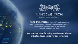
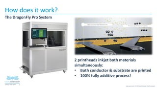
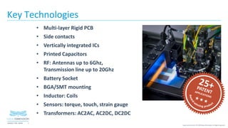
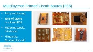
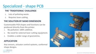
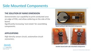
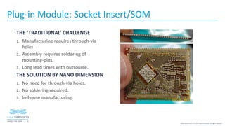
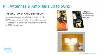
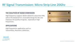
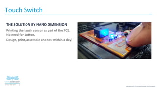
Key Technologies & Value added Applications
June 2019
www.nano-di.com
2NASDAQ / TASE :NNDM
www.nano-di.com | © 2019 Nano Dimension. All rights reserved.
Forward Looking Statements
This presentation of Nano Dimension Ltd. (the “Company”) contains “forward-looking statements” within the meaning of the Private
Securities Litigation Reform Act and other securities laws. Words such as “expects,” “anticipates,” “intends,” “plans,” “believes,” “seeks,”
“estimates” and similar expressions or variations of such words are intended to identify forward-looking statements. For example, the
Company is using forward-looking statements when it discuss the potential of it’s products. Forward-looking statements are not historical
facts, and are based upon management’s current expectations, beliefs and projections, many of which, by their nature, are inherently
uncertain. Such expectations, beliefs and projections are expressed in good faith. However, there can be no assurance that management’s
expectations, beliefs and projections will be achieved and actual results may differ materially from what is expressed in or indicated by
the forward-looking statements. Forward-looking statements are subject to risks and uncertainties that could cause actual performance
or results to differ materially from those expressed in the forward-looking statements. For a more detailed description of the risks and
uncertainties affecting the Company, reference is made to the Company’s reports filed from time to time with the Securities and
Exchange Commission (“SEC”), including, but not limited to, the risks detailed in the Company’s annual report for the year ended
December 31, 2018, filed with the SEC. Forward-looking statements speak only as of the date the statements are made. The Company
assumes no obligation to update forward-looking statements to reflect actual results, subsequent events or circumstances, changes in
assumptions or changes in other factors affecting forward-looking information except to the extent required by applicable securities laws.
If the Company does update one or more forward-looking statements, no inference should be drawn that the Company will make
additional updates with respect thereto or with respect to other forward-looking statements.
3NASDAQ / TASE :NNDM
www.nano-di.com | © 2019 Nano Dimension. All rights reserved.
3NASDAQ / TASE :NNDM
Nano Dimension is the world’s leading additive
electronics provider, targeting the growing demand for
sophisticated electronic devices that rely on
sensors, antennas and PCBs
Our additive manufacturing solutions are mission
critical and economical for our customers
www.nano-di.com | © 2019 Nano Dimension. All rights reserved.
4NASDAQ / TASE :NNDM
www.nano-di.com | © 2019 Nano Dimension. All rights reserved.
How does it work?
The DragonFly Pro System
2 printheads inkjet both materials
simultaneously:
• Both conductor & substrate are printed
• 100% fully additive process!
5NASDAQ / TASE :NNDM
www.nano-di.com | © 2019 Nano Dimension. All rights reserved.
Key Technologies
www.nano-di.com | © 2019 Nano Dimension. All rights reserved.
• Multi-layer Rigid PCB
• Side contacts
• Vertically integrated ICs
• Printed Capacitors
• RF: Antennas up to 6Ghz,
Transmission line up to 20Ghz
• Battery Socket
• BGA/SMT mounting
• Inductor: Coils
• Sensors: torque, touch, strain gauge
• Transformers: AC2AC, AC2DC, DC2DC
6NASDAQ / TASE :NNDM
www.nano-di.com | © 2019 Nano Dimension. All rights reserved.
Multilayered Printed Circuit Boards (PCB)
• Fast prototyping
• Tens of layers
in a 3mm PCB
• Reducing weeks
into hours
• Filled vias:
No need for drill
7NASDAQ / TASE :NNDM
www.nano-di.com | © 2019 Nano Dimension. All rights reserved.
Specialized - shape PCB
THE ‘TRADITIONAL’ CHALLENGE
1. Lots of polluting waste.
2. Requires laser cutting.
THE SOLUTION BY NANO DIMENSION
Customizable PCB shapes and functions can be
produced directly from the printer.
1. No pollution: 100% additive.
2. No need for external laser cutting equipment.
3. Enables a wider range of geometries.
APPLICATION
Any sensors, actuator control systems, conformal
shape designs.
8NASDAQ / TASE :NNDM
www.nano-di.com | © 2019 Nano Dimension. All rights reserved.
Side Mounted Components
THE SOLUTION BY NANO DIMENSION
Demonstrates our capability to print conducted area
on-edge of PCB, and allow soldering on the side of the
board.
Significantly increasing ‘real estate’ for assembling
components.
APPLICATIONS
High density sensor circuit, automotive circuit
connectors.
Board without side mounted components
Smaller board with side mounted components
9NASDAQ / TASE :NNDM
www.nano-di.com | © 2019 Nano Dimension. All rights reserved.
Plug-in Module: Socket Insert/SOM
THE ‘TRADITIONAL’ CHALLENGE
1. Manufacturing requires through-via
holes.
2. Assembly requires soldering of
mounting-pins.
3. Long lead times with outsource.
THE SOLUTION BY NANO DIMENSION
1. No need for through-via holes.
2. No soldering required.
3. In-house manufacturing.
10NASDAQ / TASE :NNDM
www.nano-di.com | © 2019 Nano Dimension. All rights reserved.
RF: Antennas & Amplifiers up to 6Ghz
THE SOLUTION BY NANO DIMENSION
Demonstrates our capability to print UHF &
SHF RF signal transmission line and antennas.
RF antennas & amplifier applications with up
to 6GHz frequency.
A 3D printed
transceiver next
to a traditionally
made one
11NASDAQ / TASE :NNDM
www.nano-di.com | © 2019 Nano Dimension. All rights reserved.
RF Signal Transmission: Micro Strip Line 20Ghz
THE SOLUTION BY NANO DIMENSION
High frequency support: Better dielectric value than FR4,
with 2.79 instead of 4.7. A versatile design for the vias
improves the quality of signals, especially in high
frequencies.
APPLICATIONS
High frequencies application such as
Transmitters, Receivers, Antennas.
12NASDAQ / TASE :NNDM
www.nano-di.com | © 2019 Nano Dimension. All rights reserved.
Touch Switch
THE SOLUTION BY NANO DIMENSION
Printing the touch sensor as part of the PCB.
No need for button.
Design, print, assemble and test within a day!
13NASDAQ / TASE :NNDM
www.nano-di.com | © 2019 Nano Dimension. All rights reserved.
Harris Corporation: RF Amplifier to Space
“Results showed similar RF performance between the 3D
printed version and the baseline amplifier, clearly
demonstrating the viability of 3D printed electronics for RF
circuitry.”
- Dr. Arthur Paolella, Senior scientist, Space & Intelligence
Systems, Harris Corporation
Joint project for space systems communication satellites:
3D Printed RF antenna designed to operate at 5.2 GHz and
an RF amplifier with operation up to 6 GHz.
* https://www.harris.com/impact/2018/11/harris-to-test-3-d-printed-rf-systems-in-space
Harris’ project has been selected for flight by the
International Space Station (ISS) U.S. National
Laboratory!
14NASDAQ / TASE :NNDM
www.nano-di.com | © 2019 Nano Dimension. All rights reserved.
IoT Pack
THE ‘TRADITIONAL’ CHALLENGE
1. Purchasing of 3 different elements:
PCB, antenna, battery holder is required.
2. Assembly of all elements.
THE SOLUTION BY NANO DIMENSION
1. No purchasing of PCB, antenna and battery holder.
2. No assembly required.
15NASDAQ / TASE :NNDM
www.nano-di.com | © 2019 Nano Dimension. All rights reserved.
Printed Coil: DC To DC Converter
THE SOLUTION BY NANO DIMENSION
1. Internal printed coil within the PCB.
2. Single step print without integration.
3. More compact and ‘thinner’ lightweight.
APPLICATION
DC-DC converter circuit without external
mounted coils. Maximum voltage: 50V
16NASDAQ / TASE :NNDM
www.nano-di.com | © 2019 Nano Dimension. All rights reserved.
Printed Capacitors
THE SOLUTION BY NANO DIMENSION
Demonstrates our capability to print built-in capacitors
into PCB. Capacitor is printed. No need to assemble. Can
be located within an inner layer: more room for other
components on top.
APPLICATIONS
RF filter circuit such as band pass filter. Any circuit with
capacitors.
The sample PCB capacitors capacitance
is ~6.5pF ~4200pF
17NASDAQ / TASE :NNDM
www.nano-di.com | © 2019 Nano Dimension. All rights reserved.
Vertical Assembly: Vertically Integrated ICs
THE ‘TRADITIONAL’ CHALLENGE
ICs are normally placed on top or bottom layer
of a PCB. This requires large surface area.
THE SOLUTION BY NANO DIMENSION
POC Demonstrates our capability to dramatically
increase circuit density by combining HDI Vias and
vertically assembling Integrated circuits.
Integrate ICs within the PCB layers and use surfaces
in multiple layers.
APPLICATION
IoT miniaturization designs, PCB size reduction,
IC test boards.
Sample 4 PCB stackup: Total 8 layers
18NASDAQ / TASE :NNDM
www.nano-di.com | © 2019 Nano Dimension. All rights reserved.Nano Dimension® Copyright © 2019 Nano Dimension Ltd. Nano Dimension, DragonFly, AgCite and the DragonFly logo are trademarks of Nano Dimension. Printed June 2019 DragonFly™
Follow us:
@nanodimensiontech @3Dpcb www.nano-di.comNASDAQ: NNDM
THANK YOU

Nndm apps june019_nano dimension - additive manufacturing electronics

  • 1.
    Key Technologies &Value added Applications June 2019 www.nano-di.com
  • 2.
    2NASDAQ / TASE:NNDM www.nano-di.com | © 2019 Nano Dimension. All rights reserved. Forward Looking Statements This presentation of Nano Dimension Ltd. (the “Company”) contains “forward-looking statements” within the meaning of the Private Securities Litigation Reform Act and other securities laws. Words such as “expects,” “anticipates,” “intends,” “plans,” “believes,” “seeks,” “estimates” and similar expressions or variations of such words are intended to identify forward-looking statements. For example, the Company is using forward-looking statements when it discuss the potential of it’s products. Forward-looking statements are not historical facts, and are based upon management’s current expectations, beliefs and projections, many of which, by their nature, are inherently uncertain. Such expectations, beliefs and projections are expressed in good faith. However, there can be no assurance that management’s expectations, beliefs and projections will be achieved and actual results may differ materially from what is expressed in or indicated by the forward-looking statements. Forward-looking statements are subject to risks and uncertainties that could cause actual performance or results to differ materially from those expressed in the forward-looking statements. For a more detailed description of the risks and uncertainties affecting the Company, reference is made to the Company’s reports filed from time to time with the Securities and Exchange Commission (“SEC”), including, but not limited to, the risks detailed in the Company’s annual report for the year ended December 31, 2018, filed with the SEC. Forward-looking statements speak only as of the date the statements are made. The Company assumes no obligation to update forward-looking statements to reflect actual results, subsequent events or circumstances, changes in assumptions or changes in other factors affecting forward-looking information except to the extent required by applicable securities laws. If the Company does update one or more forward-looking statements, no inference should be drawn that the Company will make additional updates with respect thereto or with respect to other forward-looking statements.
  • 3.
    3NASDAQ / TASE:NNDM www.nano-di.com | © 2019 Nano Dimension. All rights reserved. 3NASDAQ / TASE :NNDM Nano Dimension is the world’s leading additive electronics provider, targeting the growing demand for sophisticated electronic devices that rely on sensors, antennas and PCBs Our additive manufacturing solutions are mission critical and economical for our customers www.nano-di.com | © 2019 Nano Dimension. All rights reserved.
  • 4.
    4NASDAQ / TASE:NNDM www.nano-di.com | © 2019 Nano Dimension. All rights reserved. How does it work? The DragonFly Pro System 2 printheads inkjet both materials simultaneously: • Both conductor & substrate are printed • 100% fully additive process!
  • 5.
    5NASDAQ / TASE:NNDM www.nano-di.com | © 2019 Nano Dimension. All rights reserved. Key Technologies www.nano-di.com | © 2019 Nano Dimension. All rights reserved. • Multi-layer Rigid PCB • Side contacts • Vertically integrated ICs • Printed Capacitors • RF: Antennas up to 6Ghz, Transmission line up to 20Ghz • Battery Socket • BGA/SMT mounting • Inductor: Coils • Sensors: torque, touch, strain gauge • Transformers: AC2AC, AC2DC, DC2DC
  • 6.
    6NASDAQ / TASE:NNDM www.nano-di.com | © 2019 Nano Dimension. All rights reserved. Multilayered Printed Circuit Boards (PCB) • Fast prototyping • Tens of layers in a 3mm PCB • Reducing weeks into hours • Filled vias: No need for drill
  • 7.
    7NASDAQ / TASE:NNDM www.nano-di.com | © 2019 Nano Dimension. All rights reserved. Specialized - shape PCB THE ‘TRADITIONAL’ CHALLENGE 1. Lots of polluting waste. 2. Requires laser cutting. THE SOLUTION BY NANO DIMENSION Customizable PCB shapes and functions can be produced directly from the printer. 1. No pollution: 100% additive. 2. No need for external laser cutting equipment. 3. Enables a wider range of geometries. APPLICATION Any sensors, actuator control systems, conformal shape designs.
  • 8.
    8NASDAQ / TASE:NNDM www.nano-di.com | © 2019 Nano Dimension. All rights reserved. Side Mounted Components THE SOLUTION BY NANO DIMENSION Demonstrates our capability to print conducted area on-edge of PCB, and allow soldering on the side of the board. Significantly increasing ‘real estate’ for assembling components. APPLICATIONS High density sensor circuit, automotive circuit connectors. Board without side mounted components Smaller board with side mounted components
  • 9.
    9NASDAQ / TASE:NNDM www.nano-di.com | © 2019 Nano Dimension. All rights reserved. Plug-in Module: Socket Insert/SOM THE ‘TRADITIONAL’ CHALLENGE 1. Manufacturing requires through-via holes. 2. Assembly requires soldering of mounting-pins. 3. Long lead times with outsource. THE SOLUTION BY NANO DIMENSION 1. No need for through-via holes. 2. No soldering required. 3. In-house manufacturing.
  • 10.
    10NASDAQ / TASE:NNDM www.nano-di.com | © 2019 Nano Dimension. All rights reserved. RF: Antennas & Amplifiers up to 6Ghz THE SOLUTION BY NANO DIMENSION Demonstrates our capability to print UHF & SHF RF signal transmission line and antennas. RF antennas & amplifier applications with up to 6GHz frequency. A 3D printed transceiver next to a traditionally made one
  • 11.
    11NASDAQ / TASE:NNDM www.nano-di.com | © 2019 Nano Dimension. All rights reserved. RF Signal Transmission: Micro Strip Line 20Ghz THE SOLUTION BY NANO DIMENSION High frequency support: Better dielectric value than FR4, with 2.79 instead of 4.7. A versatile design for the vias improves the quality of signals, especially in high frequencies. APPLICATIONS High frequencies application such as Transmitters, Receivers, Antennas.
  • 12.
    12NASDAQ / TASE:NNDM www.nano-di.com | © 2019 Nano Dimension. All rights reserved. Touch Switch THE SOLUTION BY NANO DIMENSION Printing the touch sensor as part of the PCB. No need for button. Design, print, assemble and test within a day!
  • 13.
    13NASDAQ / TASE:NNDM www.nano-di.com | © 2019 Nano Dimension. All rights reserved. Harris Corporation: RF Amplifier to Space “Results showed similar RF performance between the 3D printed version and the baseline amplifier, clearly demonstrating the viability of 3D printed electronics for RF circuitry.” - Dr. Arthur Paolella, Senior scientist, Space & Intelligence Systems, Harris Corporation Joint project for space systems communication satellites: 3D Printed RF antenna designed to operate at 5.2 GHz and an RF amplifier with operation up to 6 GHz. * https://www.harris.com/impact/2018/11/harris-to-test-3-d-printed-rf-systems-in-space Harris’ project has been selected for flight by the International Space Station (ISS) U.S. National Laboratory!
  • 14.
    14NASDAQ / TASE:NNDM www.nano-di.com | © 2019 Nano Dimension. All rights reserved. IoT Pack THE ‘TRADITIONAL’ CHALLENGE 1. Purchasing of 3 different elements: PCB, antenna, battery holder is required. 2. Assembly of all elements. THE SOLUTION BY NANO DIMENSION 1. No purchasing of PCB, antenna and battery holder. 2. No assembly required.
  • 15.
    15NASDAQ / TASE:NNDM www.nano-di.com | © 2019 Nano Dimension. All rights reserved. Printed Coil: DC To DC Converter THE SOLUTION BY NANO DIMENSION 1. Internal printed coil within the PCB. 2. Single step print without integration. 3. More compact and ‘thinner’ lightweight. APPLICATION DC-DC converter circuit without external mounted coils. Maximum voltage: 50V
  • 16.
    16NASDAQ / TASE:NNDM www.nano-di.com | © 2019 Nano Dimension. All rights reserved. Printed Capacitors THE SOLUTION BY NANO DIMENSION Demonstrates our capability to print built-in capacitors into PCB. Capacitor is printed. No need to assemble. Can be located within an inner layer: more room for other components on top. APPLICATIONS RF filter circuit such as band pass filter. Any circuit with capacitors. The sample PCB capacitors capacitance is ~6.5pF ~4200pF
  • 17.
    17NASDAQ / TASE:NNDM www.nano-di.com | © 2019 Nano Dimension. All rights reserved. Vertical Assembly: Vertically Integrated ICs THE ‘TRADITIONAL’ CHALLENGE ICs are normally placed on top or bottom layer of a PCB. This requires large surface area. THE SOLUTION BY NANO DIMENSION POC Demonstrates our capability to dramatically increase circuit density by combining HDI Vias and vertically assembling Integrated circuits. Integrate ICs within the PCB layers and use surfaces in multiple layers. APPLICATION IoT miniaturization designs, PCB size reduction, IC test boards. Sample 4 PCB stackup: Total 8 layers
  • 18.
    18NASDAQ / TASE:NNDM www.nano-di.com | © 2019 Nano Dimension. All rights reserved.Nano Dimension® Copyright © 2019 Nano Dimension Ltd. Nano Dimension, DragonFly, AgCite and the DragonFly logo are trademarks of Nano Dimension. Printed June 2019 DragonFly™ Follow us: @nanodimensiontech @3Dpcb www.nano-di.comNASDAQ: NNDM THANK YOU