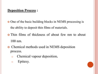
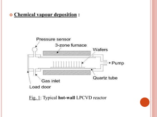
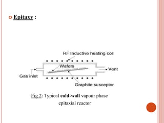
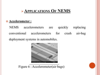
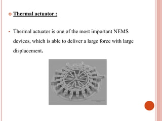
NANO-ELECTRO-MECHANICAL
SYSTEM(NEMS)
CONTENTS
 Introduction
 Benefits of Nano-machines
 Fabrication of NEMS device
 Advantages
 Applications
 Summary
 INTRODUCTION
 Nano-Electro-Mechanical system (NEMS) is the
integration of mechanical elements, sensors, actuators
and electronics on a common silicon substrate.
 The Nano mechanical components are fabricated using
compatible “micromachining” process.
 NEMS is the enabling technology allowing the
development of smart products.
 Nano electro mechanical devices promise to
revolutionize measurements of extremely small
displacement and extremely weak forces, particularly at
the molecular level.
 NEMS devices can be so small that hundreds of them
can be fit in the same space as one single micro device
that performs same function.
 In Nems devices the sensors gather the information from
surrounding environment through measuring
mechanical, chemical, biological, chemical and optical
phenomenon.
 The electronics then process the information derived
form the sensors.
 Through some decision making capability direct the
actuators to respond by moving, regulating and filtering.
 BENEFITS OF NANO MACHINES
 Nano-Mechanical devices promise to revolutionize
measurements of extremely small displacements and
forces.
 Can built with the masses approaching a few
attograms(10-18g) and with the cross section of 10nm.
 A second important attribute Nano machines is that they
dissipate less energy.
 NEMS are extremely sensitive for the external damping
mechanisms which is crucial for building sensors.
 The Geometry of a NEMS device can be tailored so that
the vibrating elements reacts only to external forces in a
specific direction.
 NEMS are ultra low power devices.
 Fundamental power scale is defined by the thermal
energy divided by the response time
 FABRICATION OF NEMS DEVICE
There are three Basic building blocks in NEMS
technology.
 Deposition processes.
 Lithography.
 Etching processes.
Deposition Process :
 One of the basic building blocks in NEMS processing is
the ability to deposit thin films of materials.
 Thin films of thickness of about few nm to about
100 nm.
 Chemical methods used in NEMS deposition
process.
o Chemical vapour deposition.
o Epitaxy.
 Chemical vapour deposition :
Fig. 1: Typical hot-wall LPCVD reactor
 Epitaxy :
Fig 2: Typical cold-wall vapour phase
epitaxial reactor
 Lithography :
 Lithography in the NEMS context is typically the
transfer of a pattern to a photosensitive material by
selective exposure to a radiation source such as light.
 A photosensitive material is a material that experiences a
change in its physical properties when exposed to a
radiation source.
 Pattern Transfer :
Fig 3: Transfer of a pattern to a photosensitive material
 Figure 4:a) Pattern definition in positive resist, b) Pattern definition in
negative resist.
 Alignment :
 Inorder to make useful devices the patterns for different
lithography steps that belongs to a single structure must
be aligned to one another.
 The first pattern includes a set of alignment marks.
 The first pattern alignment marks used as the reference
when positining subsequent patterns.
 Exposure :
 This parameter is required in order to achive accurate
pattern transfer from the Mask to the photo sensitive
layer.
 Different Photo resist exhibit different sensitivity to
different wavelengths
 Etching :
 It is necessary to etch the thin films previously
deposited or the substrate itself.
 There are 2 class of etching process.
 Wet etching.
 Dry etching.
 Wet etching :
 This is the simplest etching technology.
 There are complications since usually Mask is desired to
selectively etch the material.
 It requires a container with a liquid solution that dissolve
the material used.
 Some single crystall material, such as silicon, exhibits
anistropic etching in certain chemicals.
 ADVANTAGES
o Cost effectiveness.
o System integration.
o High Precision.
o Small size.
 APPLICATIONS OF NEMS
 Accelerometer :
NEMS accelerometers are quickly replacing
conventional accelerometers for crash air-bag
deployment systems in automobiles.
Figure 6 : Accelerometer(air bags)
 Nano nozzles:
 Another wide deployment of NEMS is their use as nano
nozzles that direct the ink in inkjet printers.
 They are also used to create miniature robots (nano-
robots) as well as nano-tweezers.
 NEMS have been rigorously tested in harsh
environments for defense and aerospace where they are
used as navigational gyroscopes.
 NEMS in Wireless :
 A 3G “smart” phone will require the functionality of as
many as five radios – for TDMA, CDMA, 3G,
Bluetooth and GSM operation. A huge increase in
component count is required to accomplish this demand.
 Thermal actuator :
 Thermal actuator is one of the most important NEMS
devices, which is able to deliver a large force with large
displacement.
 SUMMARY
 Nano-systems have the enabling capability and potential
similar to those of nano-processors .
 Since NEMS is a nascent and synergistic technology,
many new applications will emerge, expanding the
markets beyond that which is currently identified or
known.
 NEMS is forecasted to have growth similar to its parent
IC technology.
 For a great many applications, NEMS is sure to be the
technology of the future.
THANK YOU

nano-electro-mechanical-system-nems.ppt

  • 1.
  • 2.
    CONTENTS  Introduction  Benefitsof Nano-machines  Fabrication of NEMS device  Advantages  Applications  Summary
  • 3.
     INTRODUCTION  Nano-Electro-Mechanicalsystem (NEMS) is the integration of mechanical elements, sensors, actuators and electronics on a common silicon substrate.  The Nano mechanical components are fabricated using compatible “micromachining” process.  NEMS is the enabling technology allowing the development of smart products.
  • 4.
     Nano electromechanical devices promise to revolutionize measurements of extremely small displacement and extremely weak forces, particularly at the molecular level.  NEMS devices can be so small that hundreds of them can be fit in the same space as one single micro device that performs same function.
  • 5.
     In Nemsdevices the sensors gather the information from surrounding environment through measuring mechanical, chemical, biological, chemical and optical phenomenon.  The electronics then process the information derived form the sensors.  Through some decision making capability direct the actuators to respond by moving, regulating and filtering.
  • 6.
     BENEFITS OFNANO MACHINES  Nano-Mechanical devices promise to revolutionize measurements of extremely small displacements and forces.  Can built with the masses approaching a few attograms(10-18g) and with the cross section of 10nm.  A second important attribute Nano machines is that they dissipate less energy.
  • 7.
     NEMS areextremely sensitive for the external damping mechanisms which is crucial for building sensors.  The Geometry of a NEMS device can be tailored so that the vibrating elements reacts only to external forces in a specific direction.  NEMS are ultra low power devices.  Fundamental power scale is defined by the thermal energy divided by the response time
  • 8.
     FABRICATION OFNEMS DEVICE There are three Basic building blocks in NEMS technology.  Deposition processes.  Lithography.  Etching processes.
  • 9.
    Deposition Process : One of the basic building blocks in NEMS processing is the ability to deposit thin films of materials.  Thin films of thickness of about few nm to about 100 nm.  Chemical methods used in NEMS deposition process. o Chemical vapour deposition. o Epitaxy.
  • 10.
     Chemical vapourdeposition : Fig. 1: Typical hot-wall LPCVD reactor
  • 11.
     Epitaxy : Fig2: Typical cold-wall vapour phase epitaxial reactor
  • 12.
     Lithography : Lithography in the NEMS context is typically the transfer of a pattern to a photosensitive material by selective exposure to a radiation source such as light.  A photosensitive material is a material that experiences a change in its physical properties when exposed to a radiation source.
  • 13.
     Pattern Transfer: Fig 3: Transfer of a pattern to a photosensitive material
  • 14.
     Figure 4:a)Pattern definition in positive resist, b) Pattern definition in negative resist.
  • 15.
     Alignment : Inorder to make useful devices the patterns for different lithography steps that belongs to a single structure must be aligned to one another.  The first pattern includes a set of alignment marks.  The first pattern alignment marks used as the reference when positining subsequent patterns.
  • 16.
     Exposure : This parameter is required in order to achive accurate pattern transfer from the Mask to the photo sensitive layer.  Different Photo resist exhibit different sensitivity to different wavelengths
  • 17.
     Etching : It is necessary to etch the thin films previously deposited or the substrate itself.  There are 2 class of etching process.  Wet etching.  Dry etching.
  • 18.
     Wet etching:  This is the simplest etching technology.  There are complications since usually Mask is desired to selectively etch the material.  It requires a container with a liquid solution that dissolve the material used.  Some single crystall material, such as silicon, exhibits anistropic etching in certain chemicals.
  • 19.
     ADVANTAGES o Costeffectiveness. o System integration. o High Precision. o Small size.
  • 20.
     APPLICATIONS OFNEMS  Accelerometer : NEMS accelerometers are quickly replacing conventional accelerometers for crash air-bag deployment systems in automobiles. Figure 6 : Accelerometer(air bags)
  • 21.
     Nano nozzles: Another wide deployment of NEMS is their use as nano nozzles that direct the ink in inkjet printers.  They are also used to create miniature robots (nano- robots) as well as nano-tweezers.  NEMS have been rigorously tested in harsh environments for defense and aerospace where they are used as navigational gyroscopes.
  • 22.
     NEMS inWireless :  A 3G “smart” phone will require the functionality of as many as five radios – for TDMA, CDMA, 3G, Bluetooth and GSM operation. A huge increase in component count is required to accomplish this demand.
  • 23.
     Thermal actuator:  Thermal actuator is one of the most important NEMS devices, which is able to deliver a large force with large displacement.
  • 24.
     SUMMARY  Nano-systemshave the enabling capability and potential similar to those of nano-processors .  Since NEMS is a nascent and synergistic technology, many new applications will emerge, expanding the markets beyond that which is currently identified or known.
  • 25.
     NEMS isforecasted to have growth similar to its parent IC technology.  For a great many applications, NEMS is sure to be the technology of the future.
  • 26.