NANO ELECTRO MECHANICAL
SYSTEMS (NEMS)
What is NEMS?
 The term Nanoelectromechanical systems
or NEMS is used to describe devices
integrating electrical and mechanical
functionality on the nanoscale.
 NEMS form the logical next miniaturization
step from so-called microelectromechanical
systems, or MEMS devices.
NEMS - Definition
 NEMS is the integration of sensors, actuators,
electronics, photonics, energy, fluidics,
chemistry, and biology into a meaningful
system enabled by sub micrometer science
and engineering precision.
Nanowires
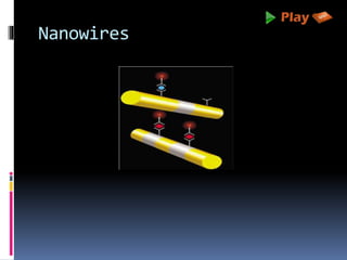
 Nanowires such as nanoLED arrays might enable a
new class of nanodisplays.
 But consider fabricating nanowires out of dissimilar
materials such as gallium arsenic on silicon.
 The ability to realize vertical nanowires composed of
metals, semiconductors, and insulators on silicon
and other substrates will enable new types of high
performance, heterogeneous micro- and
nanosystems.
 And they can be formed without the usual
considerations of lattice strain matching that occurs
in microscale dimensions.
Nanowires
NEMS in Nano Biotechnology
 NEMS will also enable other important new
opportunities in the emerging field of
nanobiotechnology.
 The ultrasensitive detection method could replace
complicated optical fluorophore tags and optical
readout methods routinely used by molecular
biologists with a simple electrically measured
parameter—frequency.
 A biocantilever diving board fabricated by Professor
Michael Roukes at CalTech has shown the ability to
detect small mass changes as low as 7 zeptograms,
which is roughly the mass of a single protein
molecule!
Nanoassembly
 The most important area of NEMS opportunity
arises— programmable self-assembly for
heterogeneous nanointegration.
 It is simply called as nanoassembly––a new
manufacturing paradigm that allows for the
directed self-assembly of components into
precise locations on a substrate.
 Nanoassembly might also be used to build
systems on non-planar or 3D surfaces where
traditional monolithic integration has failed.
Approaches to miniaturization
 Two complementary approaches to
fabrication of NEMS systems can be found.
 The top-down approach
 The bottom-up approach
Top-down approach
 The top-down approach uses the traditional
microfabrication methods, i.e. optical and
electron beam lithography, to manufacture
devices.
 Typically, devices are fabricated from metallic
thin films or etched semiconductor layers.
Bottom-up approach
 Bottom-up approaches, in contrast, use the
chemical properties of single molecules to
cause single-molecule components to
 (a) self-organize or self-assemble into some useful
conformation, or
 (b) rely on positional assembly
 This allows fabrication of much smaller
structures, albeit often at the cost of limited
control of the fabrication process.
Future of NEMS
 NEMS devices, if implemented into everyday
technologies, could further reduce the size of
modern devices and allow for better
performing sensors.
 Carbon based materials have served as prime
materials for NEMS use, because of their
highlighted mechanical and electrical
properties.
Conclusion
 In summary, the MEMS revolution that began
at DARPA in the early 1990s will continue to
bring new and more powerful microsystems
to the commercial world and defense
community.
 Therefore, there is no doubt that the Age of
NEMS will produce exciting new capabilities
we are only now beginning to imagine.
Thank You!!!
www.playppt.com

Nano electro mechanical systems

  • 1.
  • 2.
    What is NEMS? The term Nanoelectromechanical systems or NEMS is used to describe devices integrating electrical and mechanical functionality on the nanoscale.  NEMS form the logical next miniaturization step from so-called microelectromechanical systems, or MEMS devices.
  • 3.
    NEMS - Definition NEMS is the integration of sensors, actuators, electronics, photonics, energy, fluidics, chemistry, and biology into a meaningful system enabled by sub micrometer science and engineering precision.
  • 4.
    Nanowires  Nanowires suchas nanoLED arrays might enable a new class of nanodisplays.  But consider fabricating nanowires out of dissimilar materials such as gallium arsenic on silicon.  The ability to realize vertical nanowires composed of metals, semiconductors, and insulators on silicon and other substrates will enable new types of high performance, heterogeneous micro- and nanosystems.  And they can be formed without the usual considerations of lattice strain matching that occurs in microscale dimensions.
  • 5.
  • 6.
    NEMS in NanoBiotechnology  NEMS will also enable other important new opportunities in the emerging field of nanobiotechnology.  The ultrasensitive detection method could replace complicated optical fluorophore tags and optical readout methods routinely used by molecular biologists with a simple electrically measured parameter—frequency.  A biocantilever diving board fabricated by Professor Michael Roukes at CalTech has shown the ability to detect small mass changes as low as 7 zeptograms, which is roughly the mass of a single protein molecule!
  • 7.
    Nanoassembly  The mostimportant area of NEMS opportunity arises— programmable self-assembly for heterogeneous nanointegration.  It is simply called as nanoassembly––a new manufacturing paradigm that allows for the directed self-assembly of components into precise locations on a substrate.  Nanoassembly might also be used to build systems on non-planar or 3D surfaces where traditional monolithic integration has failed.
  • 8.
    Approaches to miniaturization Two complementary approaches to fabrication of NEMS systems can be found.  The top-down approach  The bottom-up approach
  • 9.
    Top-down approach  Thetop-down approach uses the traditional microfabrication methods, i.e. optical and electron beam lithography, to manufacture devices.  Typically, devices are fabricated from metallic thin films or etched semiconductor layers.
  • 10.
    Bottom-up approach  Bottom-upapproaches, in contrast, use the chemical properties of single molecules to cause single-molecule components to  (a) self-organize or self-assemble into some useful conformation, or  (b) rely on positional assembly  This allows fabrication of much smaller structures, albeit often at the cost of limited control of the fabrication process.
  • 11.
    Future of NEMS NEMS devices, if implemented into everyday technologies, could further reduce the size of modern devices and allow for better performing sensors.  Carbon based materials have served as prime materials for NEMS use, because of their highlighted mechanical and electrical properties.
  • 12.
    Conclusion  In summary,the MEMS revolution that began at DARPA in the early 1990s will continue to bring new and more powerful microsystems to the commercial world and defense community.  Therefore, there is no doubt that the Age of NEMS will produce exciting new capabilities we are only now beginning to imagine.
  • 13.