Downloaded 14 times

![Intel Desktop Board D865GSA Technical Product Specification
10
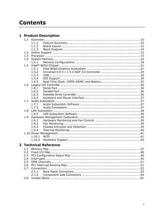
1.1 Overview
1.1.1 Feature Summary
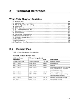
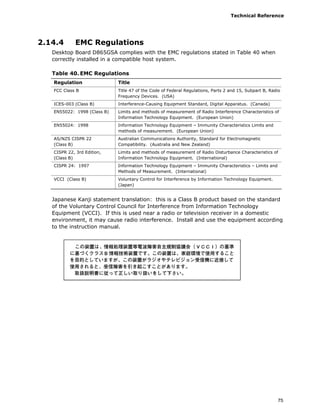
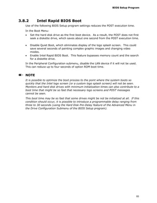
Table 1 summarizes the major features of the Desktop Board D865GSA.
Table 1. Feature Summary
Form Factor microATX (9.60 inches by 8.80 inches [243.84 millimeters by 223.52 millimeters])
Processor Support for the following:
• Intel® Pentium® D processor in an LGA775 socket with an 800 MHz system bus
• Intel® Pentium® 4 processor in an LGA775 socket with an 800 or 533 MHz
system bus
• Intel® Celeron® D processor in an LGA775 socket with a 533 MHz system bus
Memory • Two 184-pin DDR SDRAM Dual Inline Memory Module (DIMM) sockets
• Support for DDR 400, DDR 333, and DDR 266
• Support for up to 2 GB of system memory
Chipset Intel® 865G Chipset, consisting of:
• Intel® 82865G Graphics and Memory Controller Hub (GMCH)
• Intel® 82801EB I/O Controller Hub (ICH5)
• 4 Mbit Firmware Hub (FWH)
Video Intel® Extreme Graphics 2 controller
Audio Audio subsystem for AC ‘97 processing using the Realtek* ALC655 codec
Legacy I/O Control Winbond* W83627EHG LPC Bus I/O controller
USB Support for USB 2.0 devices
Peripheral
Interfaces
• Eight USB ports
• One serial port
• One parallel port
• Two Serial ATA IDE interfaces
• Two Parallel ATA IDE interfaces with UDMA 33, ATA-66/100 support
• One diskette drive interface
• PS/2* keyboard and mouse ports
LAN Support 10/100 Mbits/sec LAN subsystem using the Realtek RTL8100C Ethernet LAN
controller
continued](https://image.slidesharecdn.com/inteldesktopboard-140401131324-phpapp02/85/Intel-desktop-board-10-320.jpg)
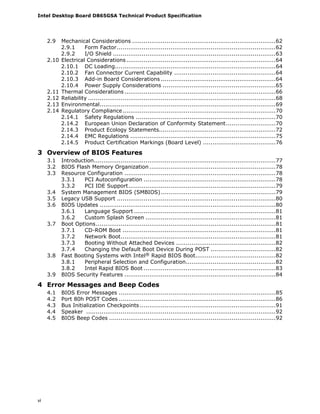
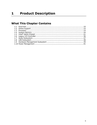
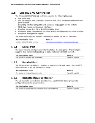
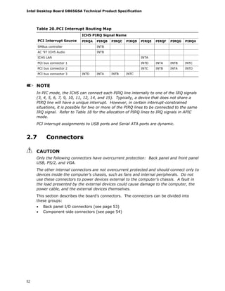
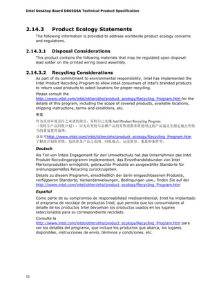
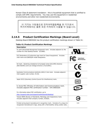
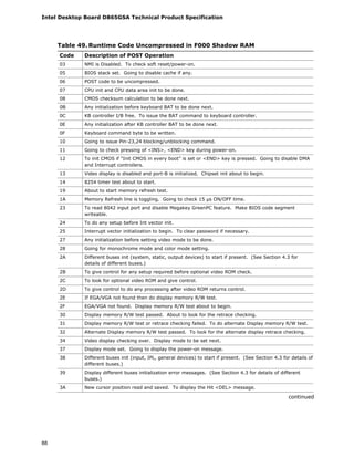
![Product Description
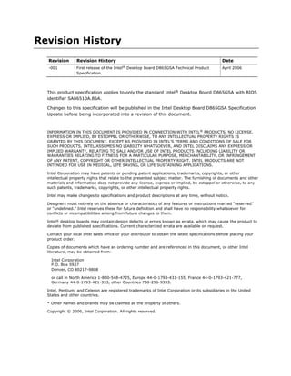
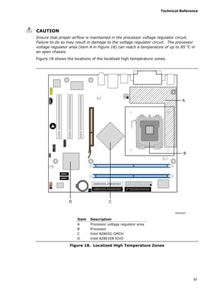
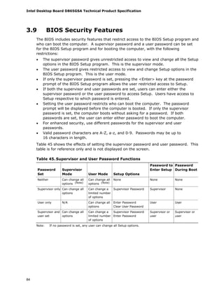
13
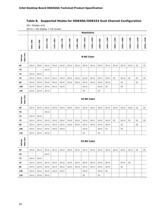
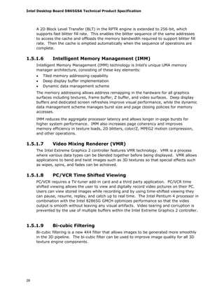
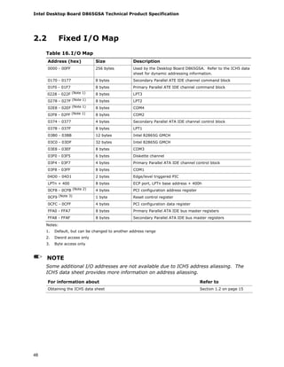
Table 2. Board Components Shown in Figure 1
Item/callout
from Figure 1 Description
A Audio codec
B Ethernet LAN controller
C AGP connector
D Rear chassis fan connector
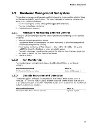
E Back panel connectors
F +12V power connector (ATX12V)
G Intel 82865G GMCH
H LGA775 processor socket
I Processor fan connector
J DIMM Channel A socket
K DIMM Channel B socket
L Legacy I/O controller
M Main Power connector
N Diskette drive connector
O Parallel ATE IDE connectors [2]
P Chassis intrusion connector
Q Battery
R Serial ATA connectors [2]
S 4 Mbit Firmware Hub (FWH)
T Front panel connector
U Intel 82801EB I/O Controller Hub (ICH5)
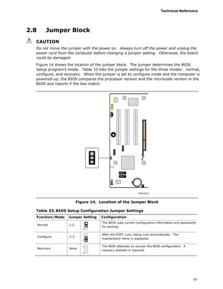
V Front chassis fan connector
W BIOS Setup configuration jumper block
X Front panel USB connector
Y Front panel USB connector
Z Speaker
AA PCI Conventional bus add-in card connectors [3]
BB ATAPI CD-ROM connector
CC Front panel audio connector](https://image.slidesharecdn.com/inteldesktopboard-140401131324-phpapp02/85/Intel-desktop-board-13-320.jpg)
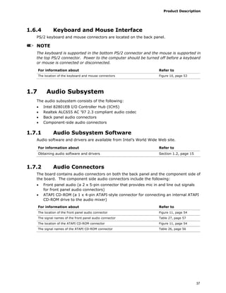
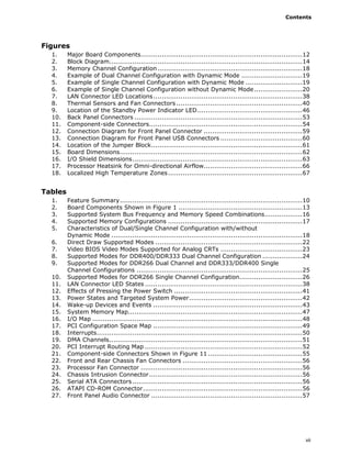
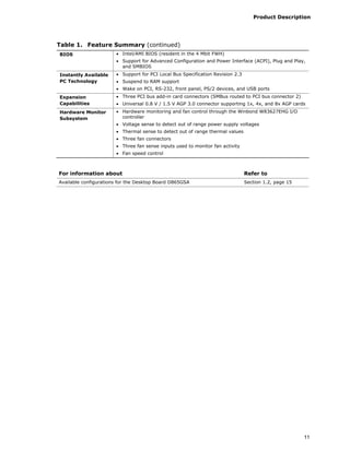
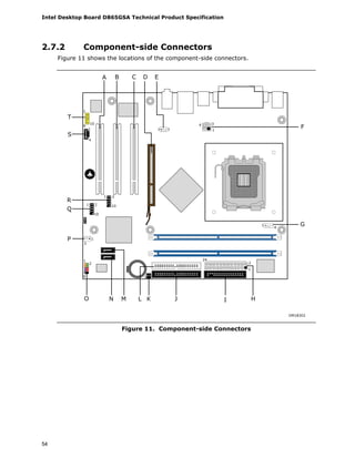
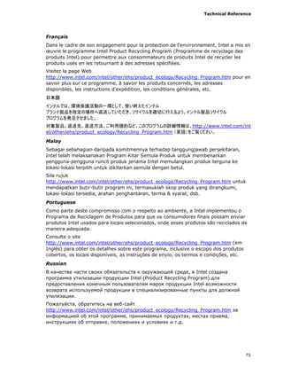
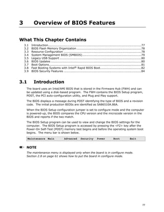
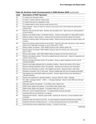
![Technical Reference
53
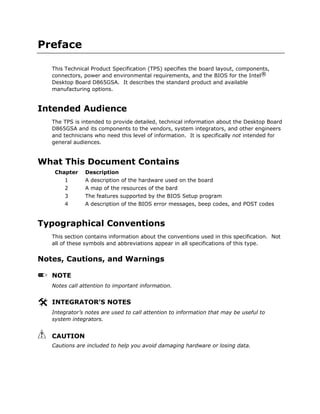
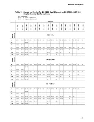
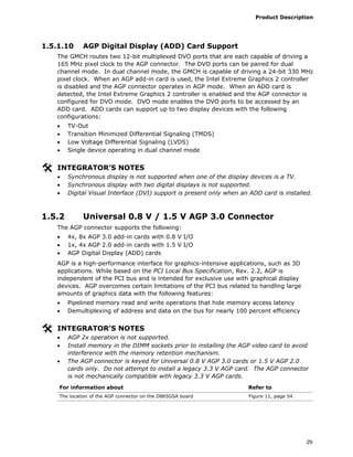
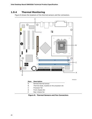
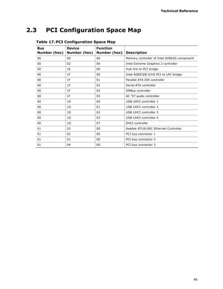
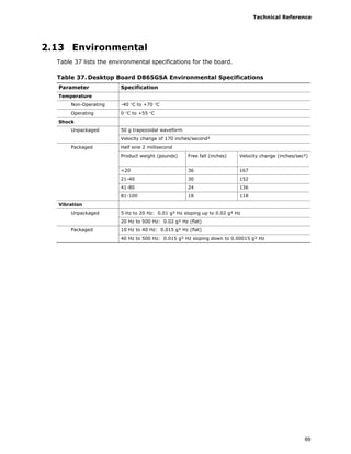
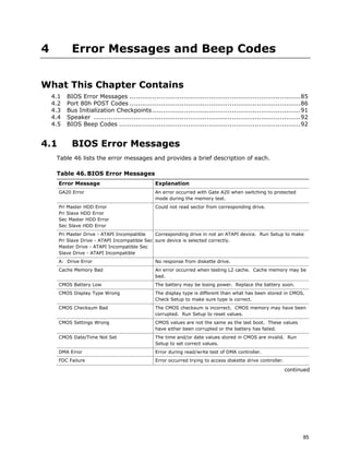
2.7.1 Back Panel Connectors
Figure 10 shows the location of the back panel connectors. The back panel connectors
are color-coded. The figure legend lists the colors used.
A
B
C
D E F G J K
H I
OM18301
Item Description Color
A PS/2 mouse port Green
B PS/2 keyboard port Purple
C Parallel port Burgundy
D Serial port A Teal
E VGA port Dark blue
F USB ports [2] Black
G USB ports [2] Black
H LAN Black
I Audio line in Light blue
J Mic in Pink
K Audio line out Lime green
Figure 10. Back Panel Connectors
NOTE
The back panel audio line out connector is designed to power headphones or amplified
speakers only. Poor audio quality occurs if passive (non-amplified) speakers are
connected to this output.](https://image.slidesharecdn.com/inteldesktopboard-140401131324-phpapp02/85/Intel-desktop-board-53-320.jpg)
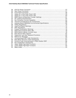
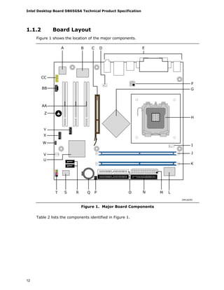
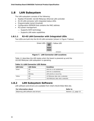
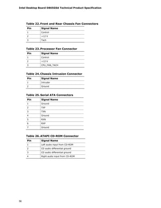
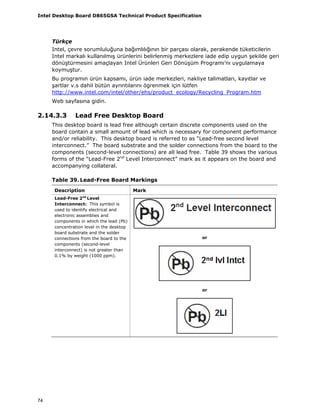
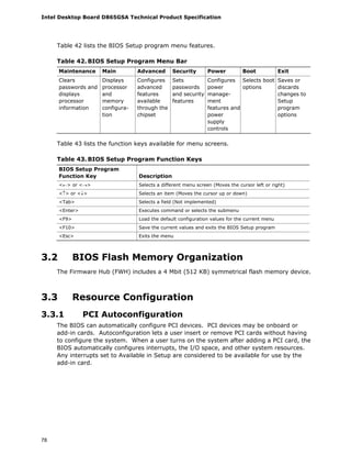
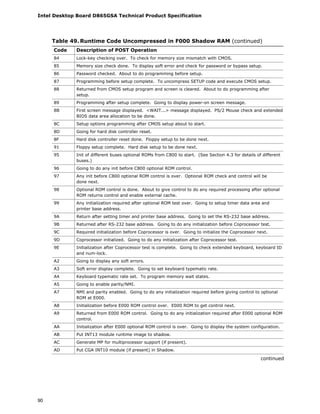
![Technical Reference
55
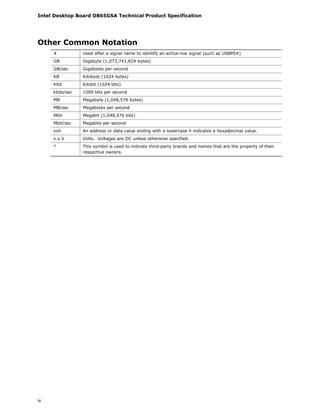
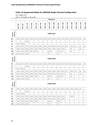
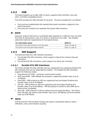
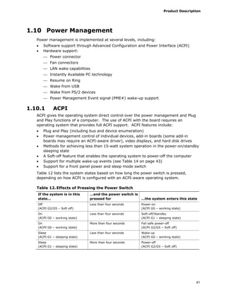
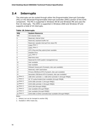
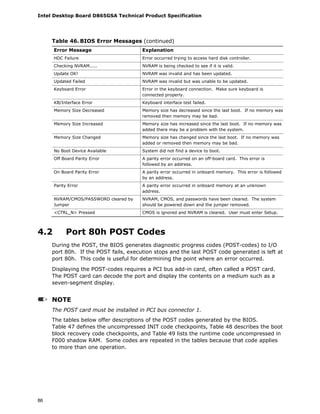
Table 21 lists the component-side connectors identified in Figure 11.
Table 21. Component-side Connectors Shown in Figure 11
Item/callout
from Figure 11 Description
A PCI Conventional bus add-in card connector 3
B PCI Conventional bus add-in card connector 2
C PCI Conventional bus add-in card connector 1
D AGP 3.0 connector
E Rear chassis fan connector
F +12V power connector (ATX12V)
G Processor fan connector
H Main power connector
I Diskette drive connector
J Primary parallel ATA IDE connector [Black]
K Chassis intrusion connector
L Secondary parallel ATA IDE connector [White]
M Serial ATA connector 0
N Serial ATA connector 1
O Front panel connector
P Front chassis fan connector
Q Front panel USB connector
R Front panel USB connector
S ATAPI CD-ROM connector
T Front panel audio connector](https://image.slidesharecdn.com/inteldesktopboard-140401131324-phpapp02/85/Intel-desktop-board-55-320.jpg)
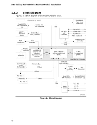
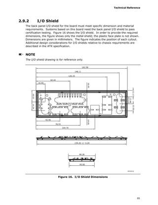
![Intel Desktop Board D865GSA Technical Product Specification
62
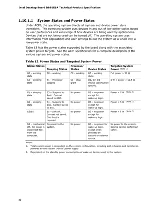
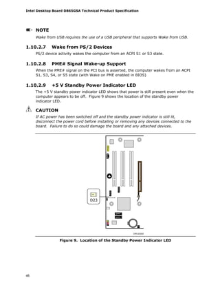
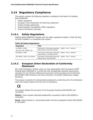
2.9 Mechanical Considerations
2.9.1 Form Factor
The board is designed to fit into either a microATX or an ATX-form-factor chassis.
Figure 15 illustrates the mechanical form factor for the board. Dimensions are given in
inches [millimeters]. The outer dimensions are 9.60 inches by 8.80 inches [243.84
millimeters by 223.52 millimeters]. Location of the I/O connectors and mounting holes
are in compliance with the ATX specification.
Figure 15. Board Dimensions](https://image.slidesharecdn.com/inteldesktopboard-140401131324-phpapp02/85/Intel-desktop-board-62-320.jpg)


The Desktop Board D865GSA supports Intel Pentium 4 and Pentium D processors, features the Intel 865G chipset, supports up to 2GB of DDR memory, includes integrated graphics and audio, and provides connectivity through USB, serial, parallel, and Ethernet ports. It also offers ACPI power management, PCI expansion slots, and hardware monitoring functions. BIOS features include Plug and Play support, boot options, and security functions.


