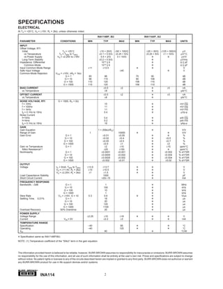
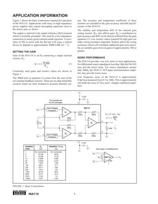
The INA114 is a low-cost, versatile instrumentation amplifier that offers excellent accuracy. It has features like low offset voltage of 50uV max, low drift of 0.25uV/°C max, and high common-mode rejection of 115dB min. An external resistor can set the gain from 1 to 10,000. It operates on a wide supply range of ±2.25V to ±18V with low power consumption of 3mA max.
Este documento describe un filtro pasa bajos que permite pasar frecuencias bajas pero atenua las altas. Utiliza un condensador de 0.22 microfaradios para presentar baja impedancia a las frecuencias altas y desviarlas, mientras que las frecuencias bajas pasan a la salida del amplificador. También explica cómo imprimir el circuito, conectarlo a un amplificador monoaural y proveerle una fuente de alimentación simétrica.
Este documento describe un protector de salidas para parlantes de amplificadores. Explica el circuito del protector, que incluye diodos, condensadores, resistencias y relevos para proteger los parlantes de sobrecargas. También incluye instrucciones para construir versiones para amplificadores de hasta 400W y hasta 1000W, así como listas de materiales y diagramas del circuito impreso.
El documento presenta los detalles de construcción de un amplificador estéreo de 500W, incluyendo un diagrama del circuito, valores recomendados de componentes, posición de los componentes en la placa de circuito impreso y una lista de materiales necesarios.
Este documento describe el diagrama eléctrico y los componentes clave de un amplificador monofónico de 250W con excelente respuesta de bajos. Incluye valores recomendados para los componentes modificables y especificaciones técnicas de los transistores utilizados como A1015, C2229, A940, C2073, 2SC5198, 2SA1941 y 2SC3858. El diagrama muestra el diseño del circuito de ganancia, preamplificación, etapas de potencia y protección del amplificador.
Este documento contiene información sobre el diagrama eléctrico y los componentes de una etapa de amplificación. Se explica que las resistencias marcadas con asteriscos son de ganancia y que la resistencia de 68K es de retroalimentación. También se proporcionan detalles sobre el número de transistores necesarios para lograr diferentes niveles de potencia de salida y sobre el voltaje requerido del transformador.
El documento proporciona un diagrama eléctrico y valores sugeridos de componentes para un amplificador monofónico de 400W. Incluye una tabla con valores modificables de componentes y su efecto. También incluye instrucciones de ensamblaje y lista de materiales necesarios para la construcción del amplificador.
Este documento proporciona los diagramas eléctrico y de conexión, así como las instrucciones de montaje y lista de materiales para un amplificador monofónico de 400W. El diagrama eléctrico muestra la disposición de los componentes electrónicos, y los valores recomendados de los componentes modificables. También incluye instrucciones sobre la colocación correcta de los componentes y la impresión de las máscaras de circuito impreso.
Este preamplificador tiene tres entradas (micrófono, línea y EQ) y un ecualizador de tres bandas, lo que lo hace ideal para karaoke. Incluye instrucciones de construcción, lista de componentes y planos para la placa de circuito impreso.
O documento descreve um amplificador de áudio profissional de alta potência chamado DBL 6000. Ele fornece até 6000 watts de potência musical total em 4 ohms e até 3600 watts em 8 ohms, com proteções térmicas e de sobrecarga. O amplificador usa ventilação forçada para resfriamento e deve ser instalado com aberturas de entrada e saída de ar.
El documento presenta los detalles de construcción de un amplificador estéreo de 500W, incluyendo un diagrama del circuito, valores recomendados de componentes, posición de los componentes en la placa de circuito impreso y una lista de materiales necesarios.
This document discusses several common radio frequency interference (RFI) and desense issues encountered in mobile devices and potential solutions. Issues covered include DDR memory clock desense, transceiver noise coupling, switching regulator noise radiating and coupling to antennas, LCD and touchscreen driver noise, and interference from USB, HDMI and other ports radiating or coupling to antennas. Solutions proposed involve modifying clock frequencies, adding decoupling capacitors, improving shielding and isolation between components, modifying circuit board layouts, and adding EMI filters.
Este documento proporciona los planos y especificaciones para construir un amplificador estéreo de 200W. Incluye un diagrama de circuito con los componentes necesarios, como transistores, diodos y condensadores, así como instrucciones para la construcción del circuito impreso y la colocación de los componentes. El amplificador puede usarse con parlantes de entre 250W y 400W máximos y funciona con una fuente de alimentación de doble voltaje de 33V.
1) El diagrama muestra un amplificador de 90W que utiliza el chip TDA7294. 2) El TDA7294 es un amplificador de potencia con alta gama de voltaje, alta potencia de salida, baja distorsión y protección contra cortocircuitos. 3) El diagrama incluye un doblador de tensión, fuente simétrica y circuito de protección para alimentar al TDA7294.
This document provides a schematic diagram for a 750 watt RMS class AB audio power amplifier designed for use with 2-ohm loudspeakers. The schematic shows the circuit layout including power supply components, input/output connections, and over 50 transistors, resistors, capacitors, diodes, and other electronic components configured to amplify audio signals. Specifications are provided listing the amplifier's maximum output power, frequency response, total harmonic distortion, input/power supply requirements, and other technical details.
Este documento proporciona información sobre un amplificador estéreo de 200W con control de tonos. Incluye diagramas esquemáticos, lista de componentes y guías de montaje. El amplificador usa un chip TA7630P para controlar los tonos y puede funcionar con cargas de 4 u 8 ohmios. Se proveen instrucciones detalladas para la construcción y montaje correctos.
Este amplificador de 250W estéreo o 125W por canal, es muy estable y da una excelente respuesta de bajos en alto volumen. Lo recomiendo!!
This amplifier 250W stereo or 125W per channel, is very stable and gives an excellent bass response at high volume. I recommend it!
Amplificador darlington de até 500 wattsGrilo Deus
Este documento descreve dois projetos de amplificador de áudio de até 500W (250+250W) usando transistores Darlington. Os transistores Darlington permitem alta potência com poucos componentes e equilíbrio de sinal. O documento explica o funcionamento, componentes, montagem e testes dos amplificadores.
Este documento presenta un circuito de control de tonos con tres bandas de frecuencia (bajos, medios y agudos) utilizando amplificadores operacionales. Describe los objetivos de identificar e implementar el circuito, así como los componentes necesarios como resistencias, condensadores, potenciómetros e integrados. Finalmente, incluye el esquema del circuito y la serigrafía para su construcción.
Este documento describe un amplificador estéreo de 400W que ofrece alta potencia y alta definición de sonido con bajo ruido. Funciona con una alimentación de ±46V CC y puede entregar 400W con 2 parlantes de 4 ohmios o 200W con 2 parlantes de 8 ohmios. Incluye diagramas del circuito, la placa de circuito impreso, la disposición de los componentes y la lista de materiales necesarios para su construcción.
Este documento presenta los diagramas esquemáticos y de conexión de un preamplificador estéreo y monofónico con control de tonos (EQ) de tres bandas (altas, medias y bajas). El circuito estéreo utiliza un integrado JRC4558 con dos amplificadores operacionales internos, mientras que el circuito mono utiliza un TL071 con un solo amplificador operacional. Ambos circuitos incluyen potenciómetros para controlar cada banda de tono y volumen, así como otros componentes comunes como resistencias, condensadores y terminales
Este documento presenta los detalles de diseño y construcción de un amplificador monofónico de 400W, incluyendo un diagrama del circuito, valores recomendados para los componentes, posiciones de montaje y una lista de materiales requeridos.
El documento presenta los diagramas y listas de componentes para construir un amplificador de 3 vías para un sistema de sonido. El amplificador utiliza circuitos integrados TL082, TL072 y 4558 para amplificar las señales de bajos, medios y altos a través de 3 canales separados. Incluye diagramas esquemáticos, de ubicación de componentes, máscaras para la placa de circuito impreso y una lista de materiales requeridos.
This document provides a listing of Philips Semiconductors small-signal transistor part numbers along with their corresponding marking codes and packaging types. It includes over 200 transistor part numbers organized by type number, marking code, and package. The marking codes are used to identify the part number during manufacturing and on the physical component. Package types include SOT23, SOT89, SOT143B, SC-59, SC-70, SC-75, and others.
Este diagrama muestra la ruta de alimentación y señal de audio para una instalación de sonido estéreo. La alimentación de 120V/220V AC se transforma a 12V DC y se distribuye a los amplificadores de 250W, preamplificadores y otros componentes. La señal de audio estéreo ingresa a los preamplificadores y se envía a los amplificadores y parlantes a través de un sumador.
Este amplificador de 250W utiliza transistores complementarios para permitir una carga de 4 ohmios. Utiliza un amplificador operacional TL071 para preamplificar la señal de entrada y proporcionar suficiente ganancia a los transistores de salida. La ganancia general puede ajustarse variando una resistencia de 33K. El amplificador es ideal para guitarra y bajo debido a su baja distorsión armónica.
The μA741 is a general-purpose operational amplifier featuring offset-voltage null capability. It has a high common-mode input voltage range, short-circuit protection, and stability without external components. The μA741 is available in various package options and is characterized for operation over different temperature ranges depending on the specific part number.
The document describes the ADS7843, a 12-bit touch screen controller with the following key features:
1) It has a 4-wire touch screen interface and ratiometric analog-to-digital conversion with 12-bit resolution up to 125 kHz conversion rate.
2) It operates from a single 2.7V to 5V supply and has low power consumption of 750uW at 125 kHz conversion rate.
3) It includes features like programmable resolution, power-down mode, and two auxiliary analog inputs, making it suitable for applications like portable devices with resistive touch screens.
The document describes the TLE2426 precision virtual ground chip. It provides a precise half the input voltage output (VO/VI ratio of 0.5) while sinking and sourcing up to 20 mA of current. It operates from an input voltage range of 4V to 40V while drawing under 400uA of supply current. It is available in various package types and temperature ranges to suit different applications.
This document provides specifications for the Mean Well ADS-55 series switching power supplies. The ADS-5512 and ADS-5524 models offer multiple DC voltage outputs, with the ADS-5512 providing 12V and 5V outputs and the ADS-5524 providing 24V and 5V outputs. Key specifications include output power range, efficiency, input voltage range, protections, standards compliance, temperature range, and dimensions.
1. The document describes the VIPer22A, a low power offline SMPS primary switcher integrated circuit that combines a current mode PWM controller with a high voltage power MOSFET.
2. The VIPer22A has a wide input voltage range of 85-265V, output power capabilities of 7-20W, and a fixed switching frequency of 60kHz.
3. It features current mode control, undervoltage lockout, overtemperature protection, and can accommodate supply voltages from 9-38V on its VDD pin.
Tank point and continuous level to base radio and back haulAsif Sheriff
The document describes a wireless tank level monitoring system. A discrete or digital level transmitter on the tank transmits the local tank level data to a base unit display within 3000 feet. The base unit then transmits the tank level data to a field office using long haul radios for monitoring on a touch screen display.
Tank point and continuous level to base radio and back haulAsif Sheriff
The document describes a wireless tank level monitoring system. A discrete or digital level transmitter on the tank transmits the local tank level data to a base unit display within 3000 feet. The base unit then transmits the tank level data to a field office using long haul radios for monitoring on a SCADA or touchscreen display.
The MUSES8920 is a high quality audio J-FET input dual operational amplifier. It has low noise of 8nV/√Hz, high slew rate of 25V/μs, and low distortion of 0.00004% at a voltage gain of 1. These characteristics make it suitable for applications such as audio preamplifiers, active filters, and line amplifiers. It can also be used in transimpedance amplifiers due to its low input bias current. The MUSES8920 is available in an 8-pin DIP or SOP package. It operates from a ±3.5V to ±16V power supply and provides high performance audio amplification.
This document summarizes the specifications of the TDA7386, a quad channel 40W car audio amplifier integrated circuit. It can provide up to 4 x 45W of power into 4 ohm loads with low distortion. It has protections for overheating, short circuits, inductive loads, and overvoltage. It requires few external components due to its integrated gain and compensation.
This document summarizes a transient voltage surge suppressor device called the ProSine PSP 120. It provides high to low level protection for sensitive electrical equipment from externally and internally generated power surges and disturbances. The PSP 120 is a NEMA LS-1 specified surge protection device that clamps transient voltages and currents across a variety of system voltages. It features threshold tracking filtering, bi-directional clamping capability, and a thermal heat sink design for long lasting performance while conforming to relevant safety standards.
The document describes a multiple output power supply design for a DVD player with the following key points:
1. It provides 7.5W of continuous output power and 13W of peak power with outputs of 3.3V, 5V, 12V, and -12V regulated using a TinySwitch-PK controller in a flyback topology.
2. It achieves good cross-regulation between the 5V and 3.3V outputs through minimizing leakage and sum regulating the feedback.
3. It includes features for EMI filtering, surge protection, clamping, and a unique peak mode for boosting current limit during peaks loads.
This document provides information on the LPC662 low power CMOS dual operational amplifier:
- It is ideal for single supply operation from +5V to +15V with rail-to-rail output swing and input common-mode range including ground.
- Key features include micropower operation (<0.5mW), high voltage gain (120dB), low input offset voltage (3mV), and ultra low input bias current (2fA).
- Applications include high-impedance buffer, precision current-to-voltage converter, long-term integrator, high-impedance preamplifier, active filter, sample-and-hold circuit, and peak detector.
The document provides data and information about the TDA8511J integrated circuit, which contains 4 single-ended power amplifiers that each produce 13 watts of output power. It has features like short-circuit protection, diagnostic capabilities, and requires few external components. The IC is intended for use in multimedia applications and active speaker systems. Key specifications are provided, along with a block diagram showing its internal components and connections.
This document summarizes a transient voltage surge suppressor device. It can provide high to low level protection for service entrances, feeders, main panels, sub panels, and distribution panels against externally and internally generated transients such as lightning surges or power fluctuations. The device has a peak surge current capacity of 60kA per phase and can protect 3-phase watt and delta systems at voltages ranging from 200-480 volts. It features an active tracking filter, bidirectional clamping capability, and low impedance hybrid circuit design to suppress voltage surges and transients.
The DRV401 is an integrated circuit designed to condition signals from closed-loop magnetic current sensors made by Vacuumschmelze GmbH & Co. KG (VAC). It provides functions like signal conditioning, an H-bridge driver for the compensation coil, and analog output proportional to primary current. The DRV401 maintains high accuracy by degaussing the sensor at power-up or on demand. It can directly drive the compensation coil or connect to external drivers. Combined with VAC sensors, the DRV401 can measure currents from small to very large.
DIP 121/120 are IP to ASI gateway devices that convert between IP and ASI transport streams. DIP 120 has two GbE inputs and two sets of six ASI outputs, while DIP 121 has one GbE input and six ASI outputs. The devices can be configured locally over a web interface or remotely using SNMP. DIP 120 also features redundant power supplies for high reliability. The gateways are used to interface IP networks with traditional broadcast infrastructure using ASI.
The LM567/LM567C are tone decoders designed to provide a saturated transistor switch output when an input signal is present within the passband. The circuit consists of an I and Q detector driven by a voltage controlled oscillator which determines the center frequency. External components independently set center frequency, bandwidth, and output delay. Features include a 20:1 frequency range adjustable with a resistor, logic compatible output, and bandwidth adjustable from 0 to 14%. Applications include touch tone decoding, frequency monitoring, FSK demodulation, and communications paging decoders.
This document provides specifications for Mean Well S-25 series switching power supplies. The S-25 series includes models that output 5V, 12V, 15V, and 24V at various current levels up to 5A. Key features include compact size, high efficiency between 72-80%, built-in EMI filtering, overload and overvoltage protection, and international AC input range from 85-264VAC. The power supplies have passed safety standards UL1012 and EN60950 and EMC standards CISPR22 and IEC801-2,3,4.
This document provides an overview of the LM118/LM218/LM318 operational amplifiers. It describes them as precision high speed operational amplifiers designed for applications requiring wide bandwidth and high slew rate, offering improved AC performance over general purpose devices. Key features highlighted include 15 MHz bandwidth, 50V/μs slew rate, and internal frequency compensation. Typical applications discussed include oscillators, active filters, sample and hold circuits, and general purpose amplifiers.
The document summarizes the specifications of the Mean Well AD-155 switching power supply series. It lists the key features such as compact size, high efficiency, overvoltage and overload protection. The specifications tables provide the electrical ratings for models AD-155A, AD-155B, and AD-155C, including output voltage, current, power, efficiency and operating conditions. Safety and EMC standards compliance are also specified.
This presentation was provided by Racquel Jemison, Ph.D., Christina MacLaughlin, Ph.D., and Paulomi Majumder. Ph.D., all of the American Chemical Society, for the second session of NISO's 2024 Training Series "DEIA in the Scholarly Landscape." Session Two: 'Expanding Pathways to Publishing Careers,' was held June 13, 2024.
Temple of Asclepius in Thrace. Excavation resultsKrassimira Luka
The temple and the sanctuary around were dedicated to Asklepios Zmidrenus. This name has been known since 1875 when an inscription dedicated to him was discovered in Rome. The inscription is dated in 227 AD and was left by soldiers originating from the city of Philippopolis (modern Plovdiv).
Philippine Edukasyong Pantahanan at Pangkabuhayan (EPP) CurriculumMJDuyan
(𝐓𝐋𝐄 𝟏𝟎𝟎) (𝐋𝐞𝐬𝐬𝐨𝐧 𝟏)-𝐏𝐫𝐞𝐥𝐢𝐦𝐬
𝐃𝐢𝐬𝐜𝐮𝐬𝐬 𝐭𝐡𝐞 𝐄𝐏𝐏 𝐂𝐮𝐫𝐫𝐢𝐜𝐮𝐥𝐮𝐦 𝐢𝐧 𝐭𝐡𝐞 𝐏𝐡𝐢𝐥𝐢𝐩𝐩𝐢𝐧𝐞𝐬:
- Understand the goals and objectives of the Edukasyong Pantahanan at Pangkabuhayan (EPP) curriculum, recognizing its importance in fostering practical life skills and values among students. Students will also be able to identify the key components and subjects covered, such as agriculture, home economics, industrial arts, and information and communication technology.
𝐄𝐱𝐩𝐥𝐚𝐢𝐧 𝐭𝐡𝐞 𝐍𝐚𝐭𝐮𝐫𝐞 𝐚𝐧𝐝 𝐒𝐜𝐨𝐩𝐞 𝐨𝐟 𝐚𝐧 𝐄𝐧𝐭𝐫𝐞𝐩𝐫𝐞𝐧𝐞𝐮𝐫:
-Define entrepreneurship, distinguishing it from general business activities by emphasizing its focus on innovation, risk-taking, and value creation. Students will describe the characteristics and traits of successful entrepreneurs, including their roles and responsibilities, and discuss the broader economic and social impacts of entrepreneurial activities on both local and global scales.
How to Setup Warehouse & Location in Odoo 17 InventoryCeline George
In this slide, we'll explore how to set up warehouses and locations in Odoo 17 Inventory. This will help us manage our stock effectively, track inventory levels, and streamline warehouse operations.
Walmart Business+ and Spark Good for Nonprofits.pdfTechSoup
"Learn about all the ways Walmart supports nonprofit organizations.
You will hear from Liz Willett, the Head of Nonprofits, and hear about what Walmart is doing to help nonprofits, including Walmart Business and Spark Good. Walmart Business+ is a new offer for nonprofits that offers discounts and also streamlines nonprofits order and expense tracking, saving time and money.
The webinar may also give some examples on how nonprofits can best leverage Walmart Business+.
The event will cover the following::
Walmart Business + (https://business.walmart.com/plus) is a new shopping experience for nonprofits, schools, and local business customers that connects an exclusive online shopping experience to stores. Benefits include free delivery and shipping, a 'Spend Analytics” feature, special discounts, deals and tax-exempt shopping.
Special TechSoup offer for a free 180 days membership, and up to $150 in discounts on eligible orders.
Spark Good (walmart.com/sparkgood) is a charitable platform that enables nonprofits to receive donations directly from customers and associates.
Answers about how you can do more with Walmart!"
This presentation was provided by Rebecca Benner, Ph.D., of the American Society of Anesthesiologists, for the second session of NISO's 2024 Training Series "DEIA in the Scholarly Landscape." Session Two: 'Expanding Pathways to Publishing Careers,' was held June 13, 2024.
2. SPECIFICATIONS
ELECTRICAL
At TA = +25°C, VS = ±15V, RL = 2kΩ, unless otherwise noted.
INA114BP, BU INA114AP, AU
PARAMETER CONDITIONS MIN TYP MAX MIN TYP MAX UNITS
INPUT
Offset Voltage, RTI
Initial TA = +25°C ±10 + 20/G ±50 + 100/G ±25 + 30/G ±125 + 500/G µV
vs Temperature TA = TMIN to TMAX ±0.1 + 0.5/G ±0.25 + 5/G ±0.25 + 5/G ±1 + 10/G µV/°C
vs Power Supply VS = ±2.25V to ±18V 0.5 + 2/G 3 + 10/G T T µV/V
Long-Term Stability ±0.2 + 0.5/G T µV/mo
Impedance, Differential 1010 || 6 T Ω || pF
Common-Mode 1010 || 6 T Ω || pF
Input Common-Mode Range ±11 ±13.5 T T V
Safe Input Voltage ±40 T V
Common-Mode Rejection VCM = ±10V, ∆RS = 1kΩ
G=1 80 96 75 90 dB
G = 10 96 115 90 106 dB
G = 100 110 120 106 110 dB
G = 1000 115 120 106 110 dB
BIAS CURRENT ±0.5 ±2 T ±5 nA
vs Temperature ±8 T pA/°C
OFFSET CURRENT ±0.5 ±2 T ±5 nA
vs Temperature ±8 T pA/°C
NOISE VOLTAGE, RTI G = 1000, RS = 0Ω
f = 10Hz 15 T nV/√Hz
f = 100Hz 11 T nV/√Hz
f = 1kHz 11 T nV/√Hz
fB = 0.1Hz to 10Hz 0.4 T µVp-p
Noise Current
f=10Hz 0.4 T pA/√Hz
f=1kHz 0.2 T pA/√Hz
fB = 0.1Hz to 10Hz 18 T pAp-p
GAIN
Gain Equation 1 + (50kΩ/RG) T V/V
Range of Gain 1 10000 T T V/V
Gain Error G=1 ±0.01 ±0.05 T T %
G = 10 ±0.02 ±0.4 T ±0.5 %
G = 100 ±0.05 ±0.5 T ±0.7 %
G = 1000 ±0.5 ±1 T ±2 %
Gain vs Temperature G=1 ±2 ±10 T ±10 ppm/°C
50kΩ Resistance(1) ±25 ±100 T T ppm/°C
Nonlinearity G=1 ±0.0001 ±0.001 T ±0.002 % of FSR
G = 10 ±0.0005 ±0.002 T ±0.004 % of FSR
G = 100 ±0.0005 ±0.002 T ±0.004 % of FSR
G = 1000 ±0.002 ±0.01 T ±0.02 % of FSR
OUTPUT
Voltage IO = 5mA, TMIN to TMAX ±13.5 ±13.7 T T V
VS = ±11.4V, RL = 2kΩ ±10 ±10.5 T T V
VS = ±2.25V, RL = 2kΩ ±1 ±1.5 T T V
Load Capacitance Stability 1000 T pF
Short Circuit Current +20/–15 T mA
FREQUENCY RESPONSE
Bandwidth, –3dB G=1 1 T MHz
G = 10 100 T kHz
G = 100 10 T kHz
G = 1000 1 T kHz
Slew Rate VO = ±10V, G = 10 0.3 0.6 T T V/µs
Settling Time, 0.01% G=1 18 T µs
G = 10 20 T µs
G = 100 120 T µs
G = 1000 1100 T µs
Overload Recovery 50% Overdrive 20 T µs
POWER SUPPLY
Voltage Range ±2.25 ±15 ±18 T T T V
Current VIN = 0V ±2.2 ±3 T T mA
TEMPERATURE RANGE
Specification –40 85 T T °C
Operating –40 125 T T °C
θJA 80 T °C/W
T Specification same as INA114BP/BU.
NOTE: (1) Temperature coefficient of the “50kΩ” term in the gain equation.
The information provided herein is believed to be reliable; however, BURR-BROWN assumes no responsibility for inaccuracies or omissions. BURR-BROWN assumes
no responsibility for the use of this information, and all use of such information shall be entirely at the user’s own risk. Prices and specifications are subject to change
without notice. No patent rights or licenses to any of the circuits described herein are implied or granted to any third party. BURR-BROWN does not authorize or warrant
any BURR-BROWN product for use in life support devices and/or systems.
®
INA114 2
3. PIN CONFIGURATIONS ELECTROSTATIC
P Package 8-Pin DIP DISCHARGE SENSITIVITY
Top View
This integrated circuit can be damaged by ESD. Burr-Brown
RG 1 8 RG recommends that all integrated circuits be handled with ap-
V–IN 2 7 V+
propriate precautions. Failure to observe proper handling and
installation procedures can cause damage.
+
V IN 3 6 VO
ESD damage can range from subtle performance degradation
V– 4 5 Ref
to complete device failure. Precision integrated circuits may
be more susceptible to damage because very small parametric
U Package SOL-16 Surface-Mount changes could cause the device not to meet its published
Top View specifications.
NC 1 16 NC
PACKAGE/ORDERING INFORMATION
RG 2 15 RG
PACKAGE
NC 3 14 NC DRAWING TEMPERATURE
PRODUCT PACKAGE NUMBER(1) RANGE
V–IN 4 13 V+
INA114AP 8-Pin Plastic DIP 006 –40°C to +85°C
V+IN 5 12 Feedback
INA114BP 8-Pin Plastic DIP 006 –40°C to +85°C
NC 6 11 VO INA114AU SOL-16 Surface-Mount 211 –40°C to +85°C
INA114BU SOL-16 Surface-Mount 211 –40°C to +85°C
V– 7 10 Ref NOTE: (1) For detailed drawing and dimension table, please see end of data
sheet, or Appendix C of Burr-Brown IC Data Book.
NC 8 9 NC
ABSOLUTE MAXIMUM RATINGS(1)
Supply Voltage .................................................................................. ±18V
Input Voltage Range .......................................................................... ±40V
Output Short-Circuit (to ground) .............................................. Continuous
Operating Temperature ................................................. –40°C to +125°C
Storage Temperature ..................................................... –40°C to +125°C
Junction Temperature .................................................................... +150°C
Lead Temperature (soldering, 10s) ............................................... +300°C
NOTE: (1) Stresses above these ratings may cause permanent damage.
®
3 INA114
4. TYPICAL PERFORMANCE CURVES
At TA = +25°C, VS = ±15V, unless otherwise noted.
GAIN vs FREQUENCY COMMON-MODE REJECTION vs FREQUENCY
140
G = 100, 1k
Common-Mode Rejection (dB)
120
1k G = 10
100
G = 1k
Gain (V/V)
100 80 G = 100
60
10
G = 10
40
1 G=1
20
0
10 100 1k 10k 100k 1M 10 100 1k 10k 100k 1M
Frequency (Hz) Frequency (Hz)
INPUT COMMON-MODE VOLTAGE RANGE POSITIVE POWER SUPPLY REJECTION
vs OUTPUT VOLTAGE vs FREQUENCY
15 140
y A1 Limit
ed b + Ou ed by A
Limit ut Swing tput 120
utp Swin2
Power Supply Rejection (dB)
10
Common-Mode Voltage (V)
+O g
–
VD/2 VO 100
5 +
– G = 1000
VD/2
+ 80
0 VCM G = 100
(Any Gain) 60 G = 10
–5 A3 – Output A3 + Output
G=1
Swing Limit Swing Limit 40
Lim
it
–10 – O ed by by A 1 g
utpu A ited in 20
t Sw 2
ing Lim put Sw
Ou t
–15 – 0
–15 –10 –5 0 5 10 15 10 100 1k 10k 100k 1M
Output Voltage (V) Frequency (Hz)
NEGATIVE POWER SUPPLY REJECTION INPUT-REFERRED NOISE VOLTAGE
vs FREQUENCY vs FREQUENCY
140 1k
Input-Referred Noise Voltage (nV/√ Hz)
120 G = 100
Power Supply Rejection (dB)
G = 1000
100
100
G=1
G = 10
80
G=1
60 G = 10
10
40 G = 100, 1000
20 G = 1000
BW Limit
0 1
10 100 1k 10k 100k 1M 1 10 100 1k 10k
Frequency (Hz) Frequency (Hz)
®
INA114 4
5. TYPICAL PERFORMANCE CURVES (CONT)
At TA = +25°C, VS = ±15V, unless otherwise noted.
SETTLING TIME vs GAIN OFFSET VOLTAGE WARM-UP vs TIME
1200 6
1000 4
Offset Voltage Change (µV)
G ≥ 100
Settling Time (µs)
800 2
600 0
0.01%
400 –2
0.1%
200 –4
0 –6
1 10 100 1000 0 15 30 45 60 75 90 105 120
Gain (V/V) Time from Power Supply Turn-on (s)
INPUT BIAS AND INPUT OFFSET CURRENT INPUT BIAS CURRENT
vs TEMPERATURE vs DIFFERENTIAL INPUT VOLTAGE
2 3
Input Bias and Input Offset Current (nA)
2
1 Input Bias Current (mA)
1
±IB
0 0
IOS
–1 G=1
–1
G = 10
–2
G = 100
G = 1000
–2 –3
–40 –15 10 35 60 85 –45 –30 –15 0 15 30 45
Temperature (°C) Differential Overload Voltage (V)
INPUT BIAS CURRENT
vs COMMON-MODE INPUT VOLTAGE MAXIMUM OUTPUT SWING vs FREQUENCY
3 32
Both Inputs 28
2 |Ib1| + |Ib2|
Peak-to-Peak Amplitude (V)
G = 1, 10
Input Bias Current (mA)
One Input 24
1 G = 100
20
Over-Voltage
0 Protection 16
Over-Voltage Normal G = 1000
Protection Operation 12
–1
8
One Input
–2
4
Both Inputs
–3 0
–45 –30 –15 0 15 30 45 10 100 1k 10k 100k 1M
Common-Mode Voltage (V) Frequency (Hz)
®
5 INA114
6. TYPICAL PERFORMANCE CURVES (CONT)
At TA = +25°C, VS = ±15V, unless otherwise noted.
SLEW RATE vs TEMPERATURE OUTPUT CURRENT LIMIT vs TEMPERATURE
1.0 30
Short Circuit Current (mA)
0.8
25
Slew Rate (V/µs)
0.6
+|ICL|
20
0.4
15
0.2 –|ICL|
0 10
–75 –50 –25 0 25 50 75 100 125 –40 –15 10 35 60 85
Temperature (°C) Temperature (°C)
QUIESCENT CURRENT AND POWER DISSIPATION
QUIESCENT CURRENT vs TEMPERATURE vs POWER SUPPLY VOLTAGE
2.8 2.6 120
2.5 100
2.6
Power Dissipation (mW)
Quiescent Current (mA)
2.4 80
2.4 Power Dissipation
2.3 60
2.2 Quiescent Current
2.2 40
2.0 2.1 20
1.8 2.0 0
–75 –50 –25 0 25 50 75 100 125 0 ±3 ±6 ±9 ±12 ±15 ±18
Temperature (°C) Power Supply Voltage (V)
POSITIVE SIGNAL SWING vs TEMPERATUE (RL = 2kΩ) NEGATIVE SIGNAL SWING vs TEMPERATUE (RL = 2kΩ)
16 –16
VS = ±15V VS = ±15V
14 –14
12 –12
VS = ±11.4V
Output Voltage (V)
Output Voltage (V)
VS = ±11.4V
10 –10
8 –8
6 –6
4 –4
VS = ±2.25V VS = ±2.25V
2 –2
0 0
–75 –50 –25 0 25 50 75 100 125 –75 –50 –25 0 25 50 75 100 125
Temperature (°C) Temperature (°C)
®
INA114 6
7. TYPICAL PERFORMANCE CURVES (CONT)
At TA = +25°C, VS = ±15V, unless otherwise noted.
LARGE SIGNAL RESPONSE, G = 1 SMALL SIGNAL RESPONSE, G = 1
+10V
+100mV
0 0
–10V –200mV
LARGE SIGNAL RESPONSE, G = 1000 SMALL SIGNAL RESPONSE, G = 1000
+10V +200mV
0 0
–10V –200mV
INPUT-REFERRED NOISE, 0.1 to 10Hz
0.1µV/div
1 s/div
®
7 INA114
8. APPLICATION INFORMATION
Figure 1 shows the basic connections required for operation ues. The accuracy and temperature coefficient of these
of the INA114. Applications with noisy or high impedance resistors are included in the gain accuracy and drift specifi-
power supplies may require decoupling capacitors close to cations of the INA114.
the device pins as shown. The stability and temperature drift of the external gain
The output is referred to the output reference (Ref) terminal setting resistor, RG, also affects gain. RG’s contribution to
which is normally grounded. This must be a low-impedance gain accuracy and drift can be directly inferred from the gain
connection to assure good common-mode rejection. A resis- equation (1). Low resistor values required for high gain can
tance of 5Ω in series with the Ref pin will cause a typical make wiring resistance important. Sockets add to the wiring
device to degrade to approximately 80dB CMR (G = 1). resistance which will contribute additional gain error (possi-
bly an unstable gain error) in gains of approximately 100 or
SETTING THE GAIN greater.
Gain of the INA114 is set by connecting a single external
resistor, RG: NOISE PERFORMANCE
The INA114 provides very low noise in most applications.
G = 1 + 50 kΩ (1) For differential source impedances less than 1kΩ, the INA103
RG
may provide lower noise. For source impedances greater
Commonly used gains and resistor values are shown in than 50kΩ, the INA111 FET-input instrumentation ampli-
Figure 1. fier may provide lower noise.
The 50kΩ term in equation (1) comes from the sum of the Low frequency noise of the INA114 is approximately
two internal feedback resistors. These are on-chip metal film 0.4µVp-p measured from 0.1 to 10Hz. This is approximately
resistors which are laser trimmed to accurate absolute val- one-tenth the noise of “low noise” chopper-stabilized ampli-
fiers.
V+
0.1µF
Pin numbers are
for DIP packages. 7
– 2 Over-Voltage INA114
VIN
Protection
A1
+ –
25kΩ 25kΩ VO = G • (VIN – VIN)
1 50kΩ
25kΩ G=1+
RG
6
RG A3
+
8
25kΩ Load VO
–
5
A2
+ 3 Over-Voltage
VIN 25kΩ 25kΩ
Protection
4 0.1µF
DESIRED RG NEAREST 1% RG
GAIN (Ω) (Ω) Also drawn in simplified form:
V–
1 No Connection No Connection
2 50.00k 49.9k V– IN
5 12.50k 12.4k INA114 VO
RG
10 5.556k 5.62k
20 2.632k 2.61k V+ IN
Ref
50 1.02k 1.02k
100 505.1 511
200 251.3 249
500 100.2 100
1000 50.05 49.9
2000 25.01 24.9
5000 10.00 10
10000 5.001 4.99
FIGURE 1. Basic Connections.
®
INA114 8
9. OFFSET TRIMMING
The INA114 is laser trimmed for very low offset voltage and
Microphone,
drift. Most applications require no external offset adjust- Hydrophone INA114
ment. Figure 2 shows an optional circuit for trimming the etc.
output offset voltage. The voltage applied to Ref terminal is
summed at the output. Low impedance must be maintained 47kΩ 47kΩ
at this node to assure good common-mode rejection. This is
achieved by buffering trim voltage with an op amp as
shown.
– Thermocouple INA114
VIN V+
VO
RG INA114
100µA
+ Ref 1/2 REF200 10kΩ
VIN
100Ω
OPA177
±10mV 10kΩ
Adjustment Range INA114
100Ω
100µA Center-tap provides
1/2 REF200 bias current return.
V– FIGURE 3. Providing an Input Common-Mode Current Path.
FIGURE 2. Optional Trimming of Output Offset Voltage.
A combination of common-mode and differential input
signals can cause the output of A1 or A2 to saturate. Figure
INPUT BIAS CURRENT RETURN PATH
4 shows the output voltage swing of A1 and A2 expressed in
The input impedance of the INA114 is extremely high— terms of a common-mode and differential input voltages.
approximately 1010Ω. However, a path must be provided for Output swing capability of these internal amplifiers is the
the input bias current of both inputs. This input bias current same as the output amplifier, A3. For applications where
is typically less than ±1nA (it can be either polarity due to input common-mode range must be maximized, limit the
cancellation circuitry). High input impedance means that output voltage swing by connecting the INA114 in a lower
this input bias current changes very little with varying input gain (see performance curve “Input Common-Mode Voltage
voltage. Range vs Output Voltage”). If necessary, add gain after the
Input circuitry must provide a path for this input bias current INA114 to increase the voltage swing.
if the INA114 is to operate properly. Figure 3 shows various Input-overload often produces an output voltage that appears
provisions for an input bias current path. Without a bias normal. For example, an input voltage of +20V on one input
current return path, the inputs will float to a potential which and +40V on the other input will obviously exceed the linear
exceeds the common-mode range of the INA114 and the common-mode range of both input amplifiers. Since both
input amplifiers will saturate. If the differential source resis- input amplifiers are saturated to nearly the same output
tance is low, bias current return path can be connected to one voltage limit, the difference voltage measured by the output
input (see thermocouple example in Figure 3). With higher amplifier will be near zero. The output of the INA114 will
source impedance, using two resistors provides a balanced be near 0V even though both inputs are overloaded.
input with possible advantages of lower input offset voltage
due to bias current and better common-mode rejection.
INPUT PROTECTION
The inputs of the INA114 are individually protected for
INPUT COMMON-MODE RANGE
voltages up to ±40V. For example, a condition of –40V on
The linear common-mode range of the input op amps of the one input and +40V on the other input will not cause
INA114 is approximately ±13.75V (or 1.25V from the damage. Internal circuitry on each input provides low series
power supplies). As the output voltage increases, however, impedance under normal signal conditions. To provide
the linear input range will be limited by the output voltage equivalent protection, series input resistors would contribute
swing of the input amplifiers, A1 and A2. The common- excessive noise. If the input is overloaded, the protection
mode range is related to the output voltage of the complete circuitry limits the input current to a safe value (approxi-
amplifier—see performance curve “Input Common-Mode mately 1.5mA). The typical performance curve “Input Bias
Range vs Output Voltage.” Current vs Common-Mode Input Voltage” shows this input
®
9 INA114
10. current limit behavior. The inputs are protected even if no The output sense connection can be used to sense the output
power supply voltage is present. voltage directly at the load for best accuracy. Figure 5 shows
how to drive a load through series interconnection resis-
OUTPUT VOLTAGE SENSE (SOL-16 package only) tance. Remotely located feedback paths may cause instabil-
ity. This can be generally be eliminated with a high
The surface-mount version of the INA114 has a separate
frequency feedback path through C1. Heavy loads or long
output sense feedback connection (pin 12). Pin 12 must be
lines can be driven by connecting a buffer inside the feed-
connected to the output terminal (pin 11) for proper opera-
back path (Figure 6).
tion. (This connection is made internally on the DIP version
of the INA114.)
V+
G • VD
VCM –
2
INA114
Over-Voltage
Protection
A1
VD 25kΩ 25kΩ 50kΩ
2 G=1+
RG
25kΩ
RG A3 VO = G • VD
25kΩ
VD
2
A2
Over-Voltage
25kΩ 25kΩ
VCM Protection
G • VD
VCM +
2
V–
FIGURE 4. Voltage Swing of A1 and A2.
Surface-mount package Surface-mount package
version only. version only.
– Output
VIN C1 –
VIN Output
Sense
1000pF Sense OPA633
RG INA114 RG IL: ±100mA
INA114
+ Ref Ref 180Ω
VIN Load +
VIN RL
Equal resistance here preserves
good common-mode rejection.
FIGURE 5. Remote Load and Ground Sensing. FIGURE 6. Buffered Output for Heavy Loads.
– VO
VIN 22.1kΩ
511Ω INA114
+
VIN 22.1kΩ
Ref
Shield is driven at the
common-mode potential. 100Ω For G = 100
RG = 511Ω // 2(22.1kΩ)
effective RG = 505Ω
OPA602
FIGURE 7. Shield Driver Circuit.
®
INA114 10
11. V+ V+
REF200
Equal line resistance here creates 100µA
a small common-mode voltage
which is rejected by INA114.
1
VO
RTD RG INA114
2
Ref
RZ
3
Resistance in this line causes VO = 0V at RRTD = RZ
a small common-mode voltage
which is rejected by INA114.
FIGURE 8. RTD Temperature Measurement Circuit.
V+
2
10.0V 6
REF102
R1
R4
27k Ω
80.6k Ω 4
1N4148 (2)
(1) R2 R7
Cu 5.23k Ω 1MΩ VO
INA114
K
Cu Ref
R3 R5
100Ω 50Ω
R6
100Ω
Zero Adj
SEEBECK
ISA COEFFICIENT R2 R4
TYPE MATERIAL (µV/°C) (R3 = 100Ω) (R5 + R6 = 100Ω)
E Chromel 58.5 3.48kΩ 56.2kΩ
Constantan
J Iron 50.2 4.12kΩ 64.9kΩ
Constantan
K Chromel 39.4 5.23kΩ 80.6kΩ
Alumel
T Copper 38.0 5.49kΩ 84.5kΩ
Constantan
NOTES: (1) –2.1mV/°C at 200µA. (2) R7 provides down-scale burn-out indication.
FIGURE 9. Thermocouple Amplifier With Cold Junction Compensation.
®
11 INA114
13. PACKAGE OPTION ADDENDUM
www.ti.com 16-Feb-2009
PACKAGING INFORMATION
Orderable Device Status (1) Package Package Pins Package Eco Plan (2) Lead/Ball Finish MSL Peak Temp (3)
Type Drawing Qty
INA114AP ACTIVE PDIP P 8 50 Green (RoHS & CU NIPDAU N / A for Pkg Type
no Sb/Br)
INA114APG4 ACTIVE PDIP P 8 50 Green (RoHS & CU NIPDAU N / A for Pkg Type
no Sb/Br)
INA114AU ACTIVE SOIC DW 16 40 Green (RoHS & CU NIPDAU Level-3-260C-168 HR
no Sb/Br)
INA114AU/1K ACTIVE SOIC DW 16 1000 Green (RoHS & CU NIPDAU Level-3-260C-168 HR
no Sb/Br)
INA114AU/1KE4 ACTIVE SOIC DW 16 1000 Green (RoHS & CU NIPDAU Level-3-260C-168 HR
no Sb/Br)
INA114AUE4 ACTIVE SOIC DW 16 40 Green (RoHS & CU NIPDAU Level-3-260C-168 HR
no Sb/Br)
INA114AUG4 ACTIVE SOIC DW 16 40 Green (RoHS & CU NIPDAU Level-3-260C-168 HR
no Sb/Br)
INA114BP ACTIVE PDIP P 8 50 Green (RoHS & CU NIPDAU N / A for Pkg Type
no Sb/Br)
INA114BPG4 ACTIVE PDIP P 8 50 Green (RoHS & CU NIPDAU N / A for Pkg Type
no Sb/Br)
INA114BU ACTIVE SOIC DW 16 40 Green (RoHS & CU NIPDAU Level-3-260C-168 HR
no Sb/Br)
INA114BU/1K ACTIVE SOIC DW 16 1000 Green (RoHS & CU NIPDAU Level-3-260C-168 HR
no Sb/Br)
INA114BU/1KE4 ACTIVE SOIC DW 16 1000 Green (RoHS & CU NIPDAU Level-3-260C-168 HR
no Sb/Br)
INA114BUE4 ACTIVE SOIC DW 16 40 Green (RoHS & CU NIPDAU Level-3-260C-168 HR
no Sb/Br)
(1)
The marketing status values are defined as follows:
ACTIVE: Product device recommended for new designs.
LIFEBUY: TI has announced that the device will be discontinued, and a lifetime-buy period is in effect.
NRND: Not recommended for new designs. Device is in production to support existing customers, but TI does not recommend using this part in
a new design.
PREVIEW: Device has been announced but is not in production. Samples may or may not be available.
OBSOLETE: TI has discontinued the production of the device.
(2)
Eco Plan - The planned eco-friendly classification: Pb-Free (RoHS), Pb-Free (RoHS Exempt), or Green (RoHS & no Sb/Br) - please check
http://www.ti.com/productcontent for the latest availability information and additional product content details.
TBD: The Pb-Free/Green conversion plan has not been defined.
Pb-Free (RoHS): TI's terms "Lead-Free" or "Pb-Free" mean semiconductor products that are compatible with the current RoHS requirements
for all 6 substances, including the requirement that lead not exceed 0.1% by weight in homogeneous materials. Where designed to be soldered
at high temperatures, TI Pb-Free products are suitable for use in specified lead-free processes.
Pb-Free (RoHS Exempt): This component has a RoHS exemption for either 1) lead-based flip-chip solder bumps used between the die and
package, or 2) lead-based die adhesive used between the die and leadframe. The component is otherwise considered Pb-Free (RoHS
compatible) as defined above.
Green (RoHS & no Sb/Br): TI defines "Green" to mean Pb-Free (RoHS compatible), and free of Bromine (Br) and Antimony (Sb) based flame
retardants (Br or Sb do not exceed 0.1% by weight in homogeneous material)
(3)
MSL, Peak Temp. -- The Moisture Sensitivity Level rating according to the JEDEC industry standard classifications, and peak solder
temperature.
Important Information and Disclaimer:The information provided on this page represents TI's knowledge and belief as of the date that it is
provided. TI bases its knowledge and belief on information provided by third parties, and makes no representation or warranty as to the
accuracy of such information. Efforts are underway to better integrate information from third parties. TI has taken and continues to take
reasonable steps to provide representative and accurate information but may not have conducted destructive testing or chemical analysis on
Addendum-Page 1
14. PACKAGE OPTION ADDENDUM
www.ti.com 16-Feb-2009
incoming materials and chemicals. TI and TI suppliers consider certain information to be proprietary, and thus CAS numbers and other limited
information may not be available for release.
In no event shall TI's liability arising out of such information exceed the total purchase price of the TI part(s) at issue in this document sold by TI
to Customer on an annual basis.
Addendum-Page 2