SlideShare a Scribd company logo
Jordan University of Science and Technology
Electrical Engineering Department
GSM-900 Mobile JAMMER
Done By: Ahmad Jisrawi
Supervised By: Dr. Nihad Dib
1
Table of Contents
Introduction ……………………………………………………………………… 2
Mobile Jamming and Disablers Techniques……………………………………… 3
GSM-Mobile JAMMING Requirements…………………………………………. 7
Design and Implementation of GSM Mobile JAMMER………………………….11
RF-Section ………………………………………………………………..11
Voltage controlled oscillator……………………………………....12
RF-Power Amplifier………………………………………………13
Antenna…………………………………………………………....15
IF-Section………………………………………………………………... 18
Triangular wave generator……………………………………….. 18
Noise Generator…………………………………………………... 20
Signal mixer and DC-offset Circuit………………………………..21
Power Supply………………………………………………………………24
Conclusions………………………………………………………………………...26
References………………………………………………………………………….27
2
INTRODUCTION
A GSM Jammer is a device that transmit signal on the same frequency at witch the
GSM system operates, the jamming success when the mobile phones in the area where
the jammer is located are disabled.
Communication jamming devices were first developed and used by military. Where
tactical commanders use RF communications to exercise control of their forces, an enemy
has interest in those communications. This interest comes from the fundamental area of
denying the successful transport of the information from the sender to the receiver.
Nowadays the mobile jammer devices are becoming civilian products rather than
electronic warfare devices, since with the increasing number of the mobile phone users
the need to disable mobile phones in specific places where the ringing of cell phone
would be disruptive has increased. These places include worship places, university
lecture rooms, libraries, concert halls, meeting rooms, and other places where silence is
appreciated.
Mosques are example for the places were mobile jammer would be a great solution,
although mosques asks politely from prayers to disable their mobile phone during the
prayer ,see figure (1), some people forget and the ringing phone of their mobile phone
become very annoying specially during the praying time.
Figure 1: Typical sign used in places where
mobile phone are not allowed
3
Mobile Jamming and Disablers Techniques
There are different approaches to prevent mobile phones from ringing in specific area,
the main five approaches used or being developed are described in RABC Mobile &
Personal Communications Committee’s (M&PCC) meeting of June 22, 1999 [1], these
techniques are summarized in this section :
1- Type "A" Device
In this device we overpower cell phone's signal with a stronger signal, This type
of device comes equipped with several independent oscillators transmitting
‘jamming signals’ capable of blocking frequencies used by paging devices as well
as those used by cellular/PCS systems’ control channels for call establishment.
When active in a designated area, such devices will (by means of RF interference)
prevent all pagers and mobile phones located in that area from receiving and
transmitting calls. This type of device transmits only a jamming signal and has very
poor frequency selectivity, which leads to interference with a larger amount of
communication spectrum than it was originally intended to target.
Technologist Jim Mahan said, “There are two types. One is called brute force
jamming, which just blocks everything. The problem is, it’s like power-washing the
airwaves and it bleeds over into the public broadcast area. The other puts out a small
amount of interference, and you could potentially confine it within a single cell
block. You could use lots of little pockets of small jamming to keep a facility under
control.”
2- Type "B" Device
This device also called "Intelligent Cellular Disablers devices", and it does not
transmit an interfering signal on the control channels. The device basically works as
a detector, and it capable to communicate with the cellular base station. When the
4
device detects the presence of a mobile phone in the "silent" room; a prevention of
authorization of call establishment is done by the software at the base station. The
device signals the base station that the target user is in a ‘quiet’ room; therefore, do
not establish the communication. Messages can be routed to the user’s voice- mail
box, if the user subscribes to a voice- mail service. This process of detection and
interruption of call establishment is done during the interval normally reserved for
signaling and handshaking.
This intelligent device as it’s name imply can recognize emergency calls and also
can allow specific pre-registered users to use their mobile phones for a specified
duration. Although this device sounds the best solution for disabling mobile phone,
a provision is needed by the cellular/PCS service providers or provision by a third-
party working cooperatively with full support of the cellular/PCS service providers,
allowing the detector device to be integral part of the cellular/PCS systems.
3- Type "C" Device
This device also called "Intelligent Beacon Disablers ", as in the type "B" device it
does not transmit an interfering signal on the control channels.
The device, when located in a specific "silent" room, functions as a ‘beacon’ and
any compatible terminal is ordered to disable its ringer or disable its operation. In
the coverage area of the beacon only terminals which have a compatible receiver
would respond and this should be built on a separate technology from cellular/PCS,
for example Bluetooth technology. Also the handset must re-enable its normal
function as it leaves the coverage area of the beacon.
The need for intelligent handsets with a separate receiver for the beacon receiver
from the cellular/PCS receiver, make effective deployment for the type "C" device
will be problematic for many years.
5
4- Type "D" Device
This jammer is similar to type "A" , but with a receiver, so that jammer is
predominantly in receive mode and when the device detects the presence of a
mobile phone in the "silent" room; it will intelligently choose to interact and block
the cell phone by transmitting jamming signal. This jam signal would only stay on
as long as the mobile continues to make a link with the base station; otherwise there
would be no jamming transmission.
Thus this device much less electromagnetic pollution in terms of raw power
transmitted and frequency spectrum from the type "A" Jammer, and therefore much
less disruptive to passing traffic. This technique could be implemented without
cooperation from PCS/cellular providers. Also this technique has an added
advantage over Type B in that no added overhead time or effort is spent negotiating
with the cellular network.
5- Type "E" Device
This technique is using EMI suppression techniques to make a room into what is
called a Faraday cage. Although labour intensive to construct, the Faraday cage
essentially blocks, or greatly attenuates, virtually all electromagnetic radiation from
entering or leaving the cage or in this case a target room.
With current advances in EMI shielding techniques and commercially available
products one could conceivably implement this into the architecture of newly
designed buildings for so-called “quiet-conference” rooms.
Emergency calls would be blocked unless there was a way to receive and decode
the Emergency Call transmissions, pass by coax outside the room and re-
transmitted.
6
This passive configuration is currently legal in most worlds' countries for any
commercial or residential location; however some building may not allow this type
of construction. Table 1 shows a comparison between the different
Jammer/Disablers techniques.
Type
Emergency
call
Efficiency
Regularity
Approval
Implementation
"A" Blocked Low
Not
allowed
Very simple
"B" Allowed Medium Required
Complex
(Required third party
Cellular/PCS Services)
"C" Allowed High Required
Complex
(Required Intelligent Handset)
"D" Allowed Medium Required Simple
"E" Blocked
High(No signal
transmitted)
Allowed Simple
Table 1: Comparison between Jammer/Disabler Techniques
7
GSM-Mobile JAMMING Requirements
As discussed in part-2, jamming objective is to inject an interference signal into
the communications frequency so that the actual signal is completely submerged by
the interference. It is important to notice that transmission can never be totally
jammed - jamming hinders the reception at the other end. The problem here for the
jammer is that only transmitters can be found using direction finding and the
location of the target must be a specific location, usually where the jammer is
located and this is because the jamming power is never infinite.
Jamming is successful when the jamming signal denies the usability of the
communications transmission. In digital communications, the usability is denied
when the error rate of the transmission cannot be compensated by error correction.
Usually a successful jamming attack requires that the jammer power is roughly
equal to signal power at the receiver.
The effects of jamming depend on the jamming-to-signal ratio (J/S), modulation
scheme, channel coding and interleaving of the target system.
Generally Jamming-to-Signal ratio can be measured according to the following
Equation. [2]
BLRGGP
BLRGGP
S
J
jjjrrttrt
rrtrrjjrj
2
2
=
Where:
Pj = jammer power Pt = transmitter power
Gjr = antenna gain from jammer to receiver
Grj = antenna gain from receiver to Jammer
Gtr = antenna gain from transmitter to receiver
Grt = antenna gain from receiver to transmitter
8
Br = communications receiver bandwidth
Bj = jamming transmitter bandwidth
Rtr = range between communications transmitter and receiver
Rjt = range between jammer and communications receiver
Lj = jammer signal loss (including polarization mismatch)
Lr = communication signal loss
The above Equation indicates that the jammer Effective Radiated Power, which is
the product of antenna gain and output power, should be high if jamming efficiency
is required. On the other hand, in order to prevent jamming, the antenna gain toward
the communication partner should be as high as possible while the gain towards the
jammer should be as small as possible. As the equation shows, the antenna pattern,
the relation between the azimuth and the gain, is a very important aspect in
jamming.
Also as we know from Microwave and shown in the equation distance has a strong
influence on the signal loss. If the distance between jammer and receiver is doubled,
the jammer has to quadruple its output in order for the jamming to have the same
effect. It must also be noted here that jammer path loss is often different from the
communications path loss; hence gives jammer an advantage over communication
transmitters.
In the GSM network, the Base Station Subsystem (BSS) takes care of the radio
resources. In addition to Base Transceiver Station (BTS), the actual RF transceiver,
BSS consists of three parts. These are the Base Station Controller (BSC), which is in
charge of mobility management and signaling on the Air-interface between Mobile
Station (MS), the BTS, and the Air-interface between BSS and Mobile Services
Switching Center (MSC).
9
The GSM Air-interface uses two different multiplexing schemes: TDMA (Time
Division Multiple Access) and FDMA (Frequency Division Multiple Access). The
spectrum is divided into 200 kHz channels (FDMA) and each channel is divided into
8 timeslots (TDMA). Each 8 timeslot TDMA frame has duration of 4.6 ms (577
s/timeslot) [3]. The GSM transmission frequencies are presented in Table 2
Uplink Downlink
GSM 900 890-915 MHz 935-960 MHz
Table 2: GSM 900 Frequency Band
Frequency Hopping in GSM is intended for the reduction of fast fading caused by
movement of subscribers. The hopping sequence may use up to 64 different
frequencies, which is a small number compared to military FH systems designed for
avoiding jamming. Also, the speed of GSM hopping is approximately 200 hops / s;
So GSM Frequency Hopping does not provide real protection against jamming
attacks.
Although FH doesn’t help in protection against jamming, interleaving and forward
error correction scheme GSM Systems can protect GSM against pulsed jamming.
For GSM it was shown that as the specified system SNRmin is 9 dB [3], a jammer
requires a 5 dB S/J in order to successfully jam a GSM channel. The optimum GSM
SNR is 12 dB, after this point the system starts to degrade.
GSM system is capable to withstand abrupt cuts in Traffic Channel (TCH)
connections. These cuts are normally caused by propagation losses due to obstacles
such as bridges. Usually another cell could be used to hold communication when the
original BTS has disconnected. The GSM architecture provides two solutions for
this: first handover when the connection is still available, second call re-
establishment when the original connection is totally lost. Handover decisions are
10
made based on transmission quality and reception level measurements carried out by
the MS and the BTS. In jamming situations call re-establishment is probably the
procedure the network will take in order to re-connect the jammed TCH.
It is obvious that downlink jamming (i.e. Jamming the mobile station 'handset'
receiver) is easier than uplink, as the base station antenna is usually located far a way
from the MS on a tower or a high building. This makes it efficient for the jammer to
overpower the signal from BS. But the Random Access Channel (RACH) control
channels of all BTSs in the area need to be jammed in order to cut off transmission.
To cut an existing connections, the jamming has to last at least until the call re-
establishment timer at the MSC expires and the connection is released, which means
that an existing call can be cut after a few seconds of effective jamming.
The GSM RACH random access scheme is very simple: when a request is not
answered, the mobile station will repeat it after a random interval. The maximum
number of repetitions and the time between them is broadcast regularly. After a MS
has tried to request service on RACH and has been rejected, it may try to request
service from another cell. Therefore, the cells in the area should be jammed. In most
cases, the efficiency of a cellular jamming is very difficult to determine, since it
depends on many factors, which leaves the jammer confused.
11
Design and Implementation of GSM Mobile JAMMER
The Implementation of type "A" JAMMER is fairly simple, the block diagram for
this type is shown in figure (2), it shows the main parts which are: RF-section, IF-
section, and the power supply.
Figure 2: Block diagram of the mobile Jammer
1-RF-Section:
The RF-section is the most important part of the mobile jammer it consist of the
Voltage Controlled Oscillator (VCO), RF Power amplifiers, and the antenna. These
components were selected according to the desired specification of the jammer such
as the frequency range and the coverage range. Its important to note that all the
components used has 50 ohm input/output impedance, so 50 ohm microstrip was
needed for matching between the components. The width of the microstrip was
calculated using the following Equations for w/h >1: [4]
To obtain the desired output jamming power for coverage range of 20 m first we found
he jamming power required at the mobile receiver "Jr", knowing that SNRmin = 9 dB
and Smax = -15dBm (i.e. worst jamming case).[5] then from
Power
Supply
5, 9,-9 V
IF
Section
RF
Section
RF jamming
signal
12
SNRmin = S/J, where S = the signal power, J = the jamming power
Jr = -24dBm, then by invoking the free space path loss equation: [6]
F = 32.45 + 20 log(f*D), where "Ds" is distance in Km and "f" is frequency in MHz ,
for 20 m the loss equals 58 dB hence the jammer should transmit a jamming signal with
power equals : 58 dB -24dBm = 34dBm, to sustain a 20m jamming area.
1.1 - Voltage Controlled Oscillator:
The VCO is responsible for generating the RF
signal which will over power the mobile
downlink signal. The selection of the VCO was
influenced by two main factors, the frequency of
the GSM system, which will be jammed and the availability of the chip. For the
first factor which implies that the VCO should cover the frequencies from 935
MHz to 960 MHz, The MAX2623 VCO from MAXIM IC was found to be a
good choice, and fortunately the second factor was met sequentially since
MAXIM IC was willing to send two of the MAX2623 for free.
Figure 3: Maxim2623 typical connection
The MAX2623 VCO is implemented as an LC oscillator configuration,
integrating all of the tank circuitry on-chip, this makes the VCO extremely easy-
13
to-use, and the tuning input is internally connected to the varactor as shown in
figure (3). The typical output power is -3dBm, and the output was best swept
over the desired range when the input tuning voltage was around 120 KHz.
1.2 - RF Power Amplifier
To achieve the desired output power a gain stages was needed, about searching
for a suitable power amplifier I found that its easer and cheaper to look for power
amplifier from an old Mobile phones. The PF08103B Hitachi power amplifier
module from NOKIA mobile phone was sufficient to
amplify an input signal in the range 800MHz to 1GHz
by 34 dB. But its recommend in the data sheet that the
power at the input should be 1dBm. To meet this
requirement I used another power amplifier stage after
the VCO and before the Hitachi Power Amplifier module, for this stage I used the
MAR-4SM power amplifier from Mini-Circuits Company, the MAR-4SM has a
typical gain of 8 dB for the frequencies range from dc to 1 GHz, so the output
after this stage should be around 5dBm. A Typical biasing Configuration for the
MAR-4SM is shown in figure (4),the bias current is delivered from a voltage
supply Vcc (+9V in this design) through the resistor Rbias
and the RF choke (inductor). The effect of the resistor is to
reduce the effect of device voltage (Vc) variation on the bias
current by so simulating a current source. Blocking
capacitors are needed at the input and output ports. To prevent stray coupling to
other signal processing components we use a bypass capacitor at the connection
to the DC supply.
14
Figure 4: Typical biasing Configuration for the MAR-4SM
The bias current is given by the following equation:
Ibias = (Vcc - Vd) / Rbias
The design for the MAR amplifier was carried on a useful program form
AGILENT TECHNOLOGIES called APPCAD, the results are shown in figure 5
Figure 5: Biasing MAR-4SM
Now the power before the Hitachi RF amplifier is 5dBm and since 1dBm is
required; I used 4dB T-Network attenuator as shown in figure (6). [7] The
attenuator also designed to have 50 ohm characteristic impedance to easily
match the whole circuits.
15
Figure 6: T-Network Attenuator
For 4-dB attenuation and symmetric Network S12 = S21 = 0.631
(i.e. VVV 122
*631.0==
−
), and for 50 ohm characteristic impedance we
found the values of the resistors using the following equations:
50 = (R2 + 50) // (R3) + R1
0.631 = (X / (X + R1))*(50 / (50 + R1)), where X = (R2 + 50)//R3.
1.3 - Antenna
The most important part of any transmitter is the
antenna, so a suitable antenna should be selected.
The antenna used in this project is 1/4 wave
monopole antenna, and it has 50 Ohm impedance
so that the antenna is matched to the transmission
system. Also this antenna has low VSWR less
than 1.7, and a bandwidth of 150 MHz around
916 MHz center frequency which cover the mobile jammer frequency range.
The antenna gain is 2dBi. The patterns for the antenna are shown below:
(a) (b)
Figure 7: (a) Monopole Principal E-plane Pattern
(b) Monopole Principal H-plane Pattern
(Source: www.rfcafe.com)
16
Figure (8) shows the output of the VCO after the two RF amplifiers using the spectrum
analyzer, and as shown it is tuned to sweeps from 625 – 960 MHz
Figure 8: output of the mobile jammer
It is important to note that the RF-Section was implemented on FR-4 printed circuit
board (PCB) with thickness of 1/32 inches. Also RF layout issues such as good
grounding, transmission lines, and vias was taken into consideration when designing the
layout for the RF-Section. Figure (9) shows the finished PCB of the RF-Section.
Figure 9: PCB of RF section of the mobile jammer
17
The Circuit Diagram for the RF-section was done using Orcad Capture, and it is
shown in figure (10)
Figure 10: Circuit diagram for the RF-Section
18
2-IF-Section:
The function of the IF-section of the Mobile jammer is to generate the tuning signal for the
VCO in The RF-Section, which will sweep the VCO through the desired range of
frequencies. This tuning signal is generated by a triangular wave generator along with
noise generator, and then offset by proper amount so as to sweep the VCO output from the
minimum desired frequency to a maximum.
2.1- Triangular Wage Generator:
In the first revision for the mobile jammer I used operational amplifiers as
relaxation oscillator to produce square wave generator and another OP-Amp as
integrator to produce the desired triangular waveform, but since the gain-bandwidth
for most OP-Amp is law the maximum output frequency was around 20 KHz which
was not sufficient to sweep the MAXIM-VCO. The solution for this was to use 555-
Timer as ASTABLE MULTIVIBRATOR. [8]
Figure 11: 555 timer connected as oscillator
19
The 555 timer consists basically of two comparators, a flip-flop, a discharge
transistor, and a resistive voltage divider. The resistive divider is used to set the
voltage comparator levels all three comparator levels.
A 555 timer connected to operate in the astable mode as a free-running
nonsinusoidal oscillator (astable multivibrator) is shown in Figure (11). The
threshold input is connected to the trigger input. The external components Rl, R2,
and Cex form the timing circuit that sets the frequency of oscillation. The 0.01
uF capacitor connected to the control input is strictly for decoupling and has no
effect on the operation; in some cases it can be left off. Initially, when the power
is turned on, the capacitor Cext is uncharged and thus the trigger voltage (pin 2)
is at 0 V. This causes the output of the lower comparator to be high and the
output of the upper comparator to be low, forcing the output of the flip-flop, and
thus the base of Qd, low and keeping the transistor off. Now, Cext begins
charging through R1 & R2 (to obtain 50% duty cycle, one can connect a diode
parallel with R2 and choose R2 = R1 ).When the capacitor voltage reaches
1/3VCC, the lower comparator switches to its low output state, and when the
capacitor voltage reaches 2/3VCC the upper comparator switches to its high
output state. This resets the flip flop causes the base of Qd to go high, and turns
on the transistor. This sequence creates a charge path for the capacitor through
R2 and the transistor, as indicated. The cap now begins to discharge, causing the
upper comparator to go low. At the point whet capacitor discharges down to
1/3VCC, the lower comparator switches high, setting the flip flop, which makes
the base of Qd low and turns off the transistor. Another charging cycles begins,
and the entire process repeats. The result is a rectangular wave output whose
20
duty cycle depends on the values of R1 and R2. The frequency of oscillation is
given by the following formula:
( )CRR
f
ext
r
21
44.1
+
=
Using the above equation for frequency equal 110 KHz, one can found the
values of R1, R2, and Cext. Then the output was taken from the voltage on the
external capacitor which has triangular wave form. A simulation was done to
verify the operation of circuit and the output is shown in figure (12).
Figure 12: The output voltage on C ext
To avoid loading the timing circuit and changing the operating frequency, the
triangular wave on the terminal of the external capacitor was buffered using OP-
Amp.
2.2- Noise Generator:
To achieve jamming a noise signal is mixed with the triangle wave signal to
produce the tuning voltage for the VCO. The noise will help in masking the
jamming transmission, making it look like random "noise" to an outside
observer. Without the noise generator, the jamming signal is just a sweeping,
unmodulated Continuous Wave RF carrier.
21
The noise generator used in this design is based on the avalanche noise
generated by a Zener breakdown phenomenon. It is created when a PN junction
is operated in the reverse breakdown mode. The avalanche noise is very similar
to shot noise, but much more intense and has a flat frequency spectrum (white).
The magnitude of the noise is difficult to predict due to its dependence on the
materials.
Basically the noise generator circuit consists of a standard 6.8 volt Zener diode
with a small reverse current, a transistor buffer, and The National LM386 audio
amplifier which acts as a natural band-pass filter and small-signal amplifier.
The output spectrum of the noise generator is shown in figure (13)
Figure 13: White-noise generator output spectrum
(Source: www.maxim-ic.com)
2.3- Signal Mixer and DC-Offset circuits:
The triangle wave and noise signals are mixed using Op-Amp configured as
summer, see figure (14). Then a DC voltage is added to the resulted signal to
obtain the required tuning voltage using Diode-Clamper circuit. Figure (15)
shows a diode clamper circuit with Bias. To gain good clamping the RC time
22
constant selected so that it's more than ten times the period of the input
frequency, also a potentiometer was added to control the biasing voltage so as
to get the desired tuning voltage.
Figure 14: OP-Amp Summer Circuit
Figure 15: Positive Diode-Clamper with bias
The complete schematic for the IF section is shown in figure (16), and the printed
circuit board for the IF section is shown below
Figure 16: PCB of the IF section for the mobile Jammer
23
Figure 16: The complete schematic for the IF section
24
3- Power Supply
The mobile jammer was designed for fixed use, and to take its power from the regular
220V AC wall outlets. The IF & RF sections of the jammer require +5, +9, and -9 DC
Voltages. So a dc-dual polarity power supply should be designed.
Figure 17: Block diagram of dual polarity power supply
The basic parts for a power supply are rectifier, filter, and regulator. The rectifier
coverts the ac input voltage to a pulsating dc voltage and can be either half wave
rectifier and full wave rectifier, the one we use is the full wave rectifier which has the
advantage that it allows unidirectional current to the load during the entire cycle of the
input voltage and the result of the full wave rectification is an output voltage with a
frequency twice the input frequency that pulsated every half-cycle of the input. The
average value for a full wave rectifier for a sinusoidal input is given by:
VAVG = 2* VP / π
The full wave rectifier used in this project is a full-wave bridge rectifier, which uses
four diodes the peak output is given by the: VP = VPsec – 1.4, where VPsec is the output
voltage across the secondary winging of the transformer. In the project the transformer
used is 220/12, 1.5 A rating, so VAVG = 11 V and VP = 15.88 V.
The second part of the power supply is the filter which eliminate the fluctuations in
the output of the full wave rectifier so as to produce a constant dc voltage, the filter is
Transformer Rectifier Filter
+ Regulator
+5V
+ Regulator
+9V
- Regulator
- 9V
25
simply a capacitor and its chosen to be as large as possible to minimize voltage ripple
in the output.
The final part of the power supply is the regulator and it is used to provide the desired
constant dc output that is basically independent of the input voltage. Single chip
regulators were used to give +5, +9, and -9 dc voltages.
Figure 18: Circuit schematic of the power supply
Figure 19: PCB of the power supply
26
Conclusion:
In this project a GSM-900 Mobile Jammer was designed and built. The project was
tested against the two GSM-900 Networks in Jordan (i.e. Fastlink and Mobilecom) and
has proven success with average range of 10 m.
I faced a problem with tuning the VCO to the desired range, due to power supply
variation with load current, so to improve the jammer a more stable power supply
should be designed for robust operation of the device, also the power supply was not
capable to deliver the needed current for the power amplifier and this the reason for the
actual coverage range of the device was not the same as designed for.
Testing in different location shows the dependent of the jamming range on the signal
strength, for instance in low GSM coverage area the jamming range exceed 20 m. In
general the jamming attack was protected by network signal power, and having large
power jamming device the GSM network will be jammed for sure, from this
observation it can be concluded that the protection against jamming attack in the GSM
system was very weak and couldn’t withstand the simplest jamming techniques.
The main disadvantage of the mobile jammer is that the transmission of the jamming
signal which is prohibited by law in many countries, for instance the fines for this
offense can range as high as 11,000 $.Despite the legal issues the transmission of high
power signal may affect the operation of some critical devices, such as hearing
impairment hardware solution. These disadvantages will constrain the use of mobile
jammer.
27
References:
[1] Mobile & Personal Communications Committee of the Radio Advisory Board of Canada,
“Use of jammer and disabler Devices for blocking PCS, Cellular & Related Services”
http://www.rabc.ottawa.on.ca/e/Files/01pub3.pdf
[2] Braun, T.; Carle, G.; Koucheryavy, Y.; Tsaoussidis, V., Wired/Wireless Internet
Communications, Third International Conference, WWIC 2005, Xanthi, Greece, May 11-
13, 2005, Proceedings, p188.
[3] John Scourias, Overview of the Global System for Mobile Communications,
http://ccnga.uwaterloo.ca/~jscouria/GSM/gsmreport.html#1
[4] Rick Hartley, RF / Microwave PC Board Design and Layout,
www.jlab.org/accel/eecad/pdf/050rfdesign.pdf
[5] http://www.mumor.org/public/publications/ISCAS_2004_MuMo_Receiver.pdf
[6] Siwiak, K., Radiowave Propagation and Antennas for Personal Communications, Artech
House, 2nd.ed, p138.
[7] Pozar, D. M., Microwave Engineering, John Wiley and Sons, 2nd.Ed, p198.
[8] Gopalan, K. Gopal, Introduction to Digital Microelectronic Circuits, Irwin, New York,
1996. pp. 496-500.
[9] Floyd, Electronic Devices, Prentice Hall, 5th. Ed, pp.60-85
[10] Horowitz, P.; Hill, W., the Art of Electronics, 2nd. Ed, Cambridge University Press.

More Related Content

What's hot

Cellphone signal detector and jammer ppt
Cellphone signal detector and jammer pptCellphone signal detector and jammer ppt
Cellphone signal detector and jammer ppt
Amar Raj
 
Mobilejammer
MobilejammerMobilejammer
Mobilejammer
akash roy
 
Cellphone Jammer
Cellphone JammerCellphone Jammer
Cellphone Jammer
Ronson Fernandes
 
Mobile phone jammers
Mobile phone jammersMobile phone jammers
Mobile phone jammers
Taruni Kancharla
 
Cell phone jammer
Cell phone jammerCell phone jammer
Cell phone jammer
Aditya Kumar Tripathy
 
How mobile phone jammer works
How mobile phone jammer worksHow mobile phone jammer works
How mobile phone jammer works
elprocus
 
Mobile jammer by venkatesh akkisetty
Mobile jammer by venkatesh akkisettyMobile jammer by venkatesh akkisetty
Mobile jammer by venkatesh akkisetty
Venky Venkatesh
 
Cell phone jammer presentation
Cell phone jammer presentationCell phone jammer presentation
Cell phone jammer presentation
Manikandan Jeeva
 
Presentation on Jamming
Presentation on JammingPresentation on Jamming
Presentation on JammingAbdul Haseeb
 
Mobile phone jammer
Mobile phone jammerMobile phone jammer
Mobile phone jammer
Suraj Prajapati
 
MOBILE SIGNAL JAMMER
MOBILE SIGNAL JAMMERMOBILE SIGNAL JAMMER
MOBILE SIGNAL JAMMER
masoommehsoud1
 
Mobile jammer by venkatesh akkisetty
Mobile jammer by venkatesh akkisettyMobile jammer by venkatesh akkisetty
Mobile jammer by venkatesh akkisetty
Venky Venkatesh
 
Cell phone jammer ppt
Cell phone jammer ppt Cell phone jammer ppt
Cell phone jammer ppt Sameer Gupta
 
Jamming Devices and how they works?
Jamming Devices and how they works?Jamming Devices and how they works?
Jamming Devices and how they works?
xiha tareen
 

What's hot (20)

Cellphone signal detector and jammer ppt
Cellphone signal detector and jammer pptCellphone signal detector and jammer ppt
Cellphone signal detector and jammer ppt
 
Mobile Jammer report
Mobile Jammer reportMobile Jammer report
Mobile Jammer report
 
Mobilejammer
MobilejammerMobilejammer
Mobilejammer
 
Cellphone Jammer
Cellphone JammerCellphone Jammer
Cellphone Jammer
 
Mobile phone jammer
Mobile phone jammerMobile phone jammer
Mobile phone jammer
 
Mobile Jammer_2
Mobile Jammer_2Mobile Jammer_2
Mobile Jammer_2
 
Mobile phone jammers
Mobile phone jammersMobile phone jammers
Mobile phone jammers
 
Cell phone jammer ppt
Cell phone jammer pptCell phone jammer ppt
Cell phone jammer ppt
 
Cell phone jammer
Cell phone jammerCell phone jammer
Cell phone jammer
 
CELL PHONE JAMMER
CELL PHONE JAMMERCELL PHONE JAMMER
CELL PHONE JAMMER
 
How mobile phone jammer works
How mobile phone jammer worksHow mobile phone jammer works
How mobile phone jammer works
 
Mobile jammer by venkatesh akkisetty
Mobile jammer by venkatesh akkisettyMobile jammer by venkatesh akkisetty
Mobile jammer by venkatesh akkisetty
 
Cell phone jammer presentation
Cell phone jammer presentationCell phone jammer presentation
Cell phone jammer presentation
 
Presentation on Jamming
Presentation on JammingPresentation on Jamming
Presentation on Jamming
 
Mobile phone jammer
Mobile phone jammerMobile phone jammer
Mobile phone jammer
 
MOBILE SIGNAL JAMMER
MOBILE SIGNAL JAMMERMOBILE SIGNAL JAMMER
MOBILE SIGNAL JAMMER
 
Mobile jammer
Mobile jammerMobile jammer
Mobile jammer
 
Mobile jammer by venkatesh akkisetty
Mobile jammer by venkatesh akkisettyMobile jammer by venkatesh akkisetty
Mobile jammer by venkatesh akkisetty
 
Cell phone jammer ppt
Cell phone jammer ppt Cell phone jammer ppt
Cell phone jammer ppt
 
Jamming Devices and how they works?
Jamming Devices and how they works?Jamming Devices and how they works?
Jamming Devices and how they works?
 

Similar to Gsm jammer 2

Mobile jammer
Mobile jammerMobile jammer
Mobile jammer
Avay Minni
 
mobilejammer
mobilejammermobilejammer
mobilejammer
Naga Dinesh
 
mobile jammer.ppt_082549-2(1).pptx
mobile jammer.ppt_082549-2(1).pptxmobile jammer.ppt_082549-2(1).pptx
mobile jammer.ppt_082549-2(1).pptx
LingaSwamy10
 
Function of Mobile Jammer
Function of Mobile JammerFunction of Mobile Jammer
Function of Mobile Jammer
Professional Packers & Movers Pvt. Ltd.
 
Mobile Jammer
Mobile JammerMobile Jammer
Mobile Jammer
Sudhanshu kumar Sah
 
Mobile Jammer ppt
Mobile Jammer pptMobile Jammer ppt
Mobile jammer
Mobile jammerMobile jammer
Mobile jammer
Chandu Pawar
 
Govind
GovindGovind
Govind
Garima Singh
 
cell phone jammer report
cell phone jammer reportcell phone jammer report
cell phone jammer reportSameer Gupta
 
Intelligent jammer
Intelligent jammerIntelligent jammer
Intelligent jammer
Prejith Pavanan
 
FPGA Based Wireless Jamming Networks
FPGA Based Wireless Jamming NetworksFPGA Based Wireless Jamming Networks
FPGA Based Wireless Jamming Networks
IJMER
 
Wireless signal jamming
Wireless signal jammingWireless signal jamming
Wireless signal jammingMahmoud Abdeen
 
IRJET- Signal Jammer in Military Operations
IRJET-  	  Signal Jammer in Military OperationsIRJET-  	  Signal Jammer in Military Operations
IRJET- Signal Jammer in Military Operations
IRJET Journal
 
Intelligent Jammer
Intelligent JammerIntelligent Jammer
Intelligent Jammer
Prejith Pavanan
 
Best abdulmajeed extended_abstract-libre
Best abdulmajeed extended_abstract-libreBest abdulmajeed extended_abstract-libre
Best abdulmajeed extended_abstract-libre
Navin Mishra
 
A project report_at_cell_phone_detector - copy
A project report_at_cell_phone_detector - copyA project report_at_cell_phone_detector - copy
A project report_at_cell_phone_detector - copy
Pranoosh T
 
Mobile jammer ppt
Mobile jammer pptMobile jammer ppt
Mobile jammer ppt
Amit sundaray
 
Presentation1
Presentation1Presentation1
Presentation1
poojithakannikanti
 

Similar to Gsm jammer 2 (20)

Mobile jammer
Mobile jammerMobile jammer
Mobile jammer
 
mobilejammer
mobilejammermobilejammer
mobilejammer
 
mobile jammer.ppt_082549-2(1).pptx
mobile jammer.ppt_082549-2(1).pptxmobile jammer.ppt_082549-2(1).pptx
mobile jammer.ppt_082549-2(1).pptx
 
Function of Mobile Jammer
Function of Mobile JammerFunction of Mobile Jammer
Function of Mobile Jammer
 
Mobile Jammer
Mobile JammerMobile Jammer
Mobile Jammer
 
Ceplone
CeploneCeplone
Ceplone
 
Mobile Jammer ppt
Mobile Jammer pptMobile Jammer ppt
Mobile Jammer ppt
 
Mobile jammer
Mobile jammerMobile jammer
Mobile jammer
 
Govind
GovindGovind
Govind
 
cell phone jammer report
cell phone jammer reportcell phone jammer report
cell phone jammer report
 
Intelligent jammer
Intelligent jammerIntelligent jammer
Intelligent jammer
 
FPGA Based Wireless Jamming Networks
FPGA Based Wireless Jamming NetworksFPGA Based Wireless Jamming Networks
FPGA Based Wireless Jamming Networks
 
Wireless signal jamming
Wireless signal jammingWireless signal jamming
Wireless signal jamming
 
IRJET- Signal Jammer in Military Operations
IRJET-  	  Signal Jammer in Military OperationsIRJET-  	  Signal Jammer in Military Operations
IRJET- Signal Jammer in Military Operations
 
Intelligent Jammer
Intelligent JammerIntelligent Jammer
Intelligent Jammer
 
Best abdulmajeed extended_abstract-libre
Best abdulmajeed extended_abstract-libreBest abdulmajeed extended_abstract-libre
Best abdulmajeed extended_abstract-libre
 
Mobile jammer
Mobile jammerMobile jammer
Mobile jammer
 
A project report_at_cell_phone_detector - copy
A project report_at_cell_phone_detector - copyA project report_at_cell_phone_detector - copy
A project report_at_cell_phone_detector - copy
 
Mobile jammer ppt
Mobile jammer pptMobile jammer ppt
Mobile jammer ppt
 
Presentation1
Presentation1Presentation1
Presentation1
 

Recently uploaded

Smart TV Buyer Insights Survey 2024 by 91mobiles.pdf
Smart TV Buyer Insights Survey 2024 by 91mobiles.pdfSmart TV Buyer Insights Survey 2024 by 91mobiles.pdf
Smart TV Buyer Insights Survey 2024 by 91mobiles.pdf
91mobiles
 
De-mystifying Zero to One: Design Informed Techniques for Greenfield Innovati...
De-mystifying Zero to One: Design Informed Techniques for Greenfield Innovati...De-mystifying Zero to One: Design Informed Techniques for Greenfield Innovati...
De-mystifying Zero to One: Design Informed Techniques for Greenfield Innovati...
Product School
 
Empowering NextGen Mobility via Large Action Model Infrastructure (LAMI): pav...
Empowering NextGen Mobility via Large Action Model Infrastructure (LAMI): pav...Empowering NextGen Mobility via Large Action Model Infrastructure (LAMI): pav...
Empowering NextGen Mobility via Large Action Model Infrastructure (LAMI): pav...
Thierry Lestable
 
Essentials of Automations: Optimizing FME Workflows with Parameters
Essentials of Automations: Optimizing FME Workflows with ParametersEssentials of Automations: Optimizing FME Workflows with Parameters
Essentials of Automations: Optimizing FME Workflows with Parameters
Safe Software
 
Key Trends Shaping the Future of Infrastructure.pdf
Key Trends Shaping the Future of Infrastructure.pdfKey Trends Shaping the Future of Infrastructure.pdf
Key Trends Shaping the Future of Infrastructure.pdf
Cheryl Hung
 
UiPath Test Automation using UiPath Test Suite series, part 4
UiPath Test Automation using UiPath Test Suite series, part 4UiPath Test Automation using UiPath Test Suite series, part 4
UiPath Test Automation using UiPath Test Suite series, part 4
DianaGray10
 
DevOps and Testing slides at DASA Connect
DevOps and Testing slides at DASA ConnectDevOps and Testing slides at DASA Connect
DevOps and Testing slides at DASA Connect
Kari Kakkonen
 
GraphRAG is All You need? LLM & Knowledge Graph
GraphRAG is All You need? LLM & Knowledge GraphGraphRAG is All You need? LLM & Knowledge Graph
GraphRAG is All You need? LLM & Knowledge Graph
Guy Korland
 
Transcript: Selling digital books in 2024: Insights from industry leaders - T...
Transcript: Selling digital books in 2024: Insights from industry leaders - T...Transcript: Selling digital books in 2024: Insights from industry leaders - T...
Transcript: Selling digital books in 2024: Insights from industry leaders - T...
BookNet Canada
 
Leading Change strategies and insights for effective change management pdf 1.pdf
Leading Change strategies and insights for effective change management pdf 1.pdfLeading Change strategies and insights for effective change management pdf 1.pdf
Leading Change strategies and insights for effective change management pdf 1.pdf
OnBoard
 
By Design, not by Accident - Agile Venture Bolzano 2024
By Design, not by Accident - Agile Venture Bolzano 2024By Design, not by Accident - Agile Venture Bolzano 2024
By Design, not by Accident - Agile Venture Bolzano 2024
Pierluigi Pugliese
 
The Future of Platform Engineering
The Future of Platform EngineeringThe Future of Platform Engineering
The Future of Platform Engineering
Jemma Hussein Allen
 
How world-class product teams are winning in the AI era by CEO and Founder, P...
How world-class product teams are winning in the AI era by CEO and Founder, P...How world-class product teams are winning in the AI era by CEO and Founder, P...
How world-class product teams are winning in the AI era by CEO and Founder, P...
Product School
 
GDG Cloud Southlake #33: Boule & Rebala: Effective AppSec in SDLC using Deplo...
GDG Cloud Southlake #33: Boule & Rebala: Effective AppSec in SDLC using Deplo...GDG Cloud Southlake #33: Boule & Rebala: Effective AppSec in SDLC using Deplo...
GDG Cloud Southlake #33: Boule & Rebala: Effective AppSec in SDLC using Deplo...
James Anderson
 
Secstrike : Reverse Engineering & Pwnable tools for CTF.pptx
Secstrike : Reverse Engineering & Pwnable tools for CTF.pptxSecstrike : Reverse Engineering & Pwnable tools for CTF.pptx
Secstrike : Reverse Engineering & Pwnable tools for CTF.pptx
nkrafacyberclub
 
SAP Sapphire 2024 - ASUG301 building better apps with SAP Fiori.pdf
SAP Sapphire 2024 - ASUG301 building better apps with SAP Fiori.pdfSAP Sapphire 2024 - ASUG301 building better apps with SAP Fiori.pdf
SAP Sapphire 2024 - ASUG301 building better apps with SAP Fiori.pdf
Peter Spielvogel
 
Epistemic Interaction - tuning interfaces to provide information for AI support
Epistemic Interaction - tuning interfaces to provide information for AI supportEpistemic Interaction - tuning interfaces to provide information for AI support
Epistemic Interaction - tuning interfaces to provide information for AI support
Alan Dix
 
Monitoring Java Application Security with JDK Tools and JFR Events
Monitoring Java Application Security with JDK Tools and JFR EventsMonitoring Java Application Security with JDK Tools and JFR Events
Monitoring Java Application Security with JDK Tools and JFR Events
Ana-Maria Mihalceanu
 
LF Energy Webinar: Electrical Grid Modelling and Simulation Through PowSyBl -...
LF Energy Webinar: Electrical Grid Modelling and Simulation Through PowSyBl -...LF Energy Webinar: Electrical Grid Modelling and Simulation Through PowSyBl -...
LF Energy Webinar: Electrical Grid Modelling and Simulation Through PowSyBl -...
DanBrown980551
 
Builder.ai Founder Sachin Dev Duggal's Strategic Approach to Create an Innova...
Builder.ai Founder Sachin Dev Duggal's Strategic Approach to Create an Innova...Builder.ai Founder Sachin Dev Duggal's Strategic Approach to Create an Innova...
Builder.ai Founder Sachin Dev Duggal's Strategic Approach to Create an Innova...
Ramesh Iyer
 

Recently uploaded (20)

Smart TV Buyer Insights Survey 2024 by 91mobiles.pdf
Smart TV Buyer Insights Survey 2024 by 91mobiles.pdfSmart TV Buyer Insights Survey 2024 by 91mobiles.pdf
Smart TV Buyer Insights Survey 2024 by 91mobiles.pdf
 
De-mystifying Zero to One: Design Informed Techniques for Greenfield Innovati...
De-mystifying Zero to One: Design Informed Techniques for Greenfield Innovati...De-mystifying Zero to One: Design Informed Techniques for Greenfield Innovati...
De-mystifying Zero to One: Design Informed Techniques for Greenfield Innovati...
 
Empowering NextGen Mobility via Large Action Model Infrastructure (LAMI): pav...
Empowering NextGen Mobility via Large Action Model Infrastructure (LAMI): pav...Empowering NextGen Mobility via Large Action Model Infrastructure (LAMI): pav...
Empowering NextGen Mobility via Large Action Model Infrastructure (LAMI): pav...
 
Essentials of Automations: Optimizing FME Workflows with Parameters
Essentials of Automations: Optimizing FME Workflows with ParametersEssentials of Automations: Optimizing FME Workflows with Parameters
Essentials of Automations: Optimizing FME Workflows with Parameters
 
Key Trends Shaping the Future of Infrastructure.pdf
Key Trends Shaping the Future of Infrastructure.pdfKey Trends Shaping the Future of Infrastructure.pdf
Key Trends Shaping the Future of Infrastructure.pdf
 
UiPath Test Automation using UiPath Test Suite series, part 4
UiPath Test Automation using UiPath Test Suite series, part 4UiPath Test Automation using UiPath Test Suite series, part 4
UiPath Test Automation using UiPath Test Suite series, part 4
 
DevOps and Testing slides at DASA Connect
DevOps and Testing slides at DASA ConnectDevOps and Testing slides at DASA Connect
DevOps and Testing slides at DASA Connect
 
GraphRAG is All You need? LLM & Knowledge Graph
GraphRAG is All You need? LLM & Knowledge GraphGraphRAG is All You need? LLM & Knowledge Graph
GraphRAG is All You need? LLM & Knowledge Graph
 
Transcript: Selling digital books in 2024: Insights from industry leaders - T...
Transcript: Selling digital books in 2024: Insights from industry leaders - T...Transcript: Selling digital books in 2024: Insights from industry leaders - T...
Transcript: Selling digital books in 2024: Insights from industry leaders - T...
 
Leading Change strategies and insights for effective change management pdf 1.pdf
Leading Change strategies and insights for effective change management pdf 1.pdfLeading Change strategies and insights for effective change management pdf 1.pdf
Leading Change strategies and insights for effective change management pdf 1.pdf
 
By Design, not by Accident - Agile Venture Bolzano 2024
By Design, not by Accident - Agile Venture Bolzano 2024By Design, not by Accident - Agile Venture Bolzano 2024
By Design, not by Accident - Agile Venture Bolzano 2024
 
The Future of Platform Engineering
The Future of Platform EngineeringThe Future of Platform Engineering
The Future of Platform Engineering
 
How world-class product teams are winning in the AI era by CEO and Founder, P...
How world-class product teams are winning in the AI era by CEO and Founder, P...How world-class product teams are winning in the AI era by CEO and Founder, P...
How world-class product teams are winning in the AI era by CEO and Founder, P...
 
GDG Cloud Southlake #33: Boule & Rebala: Effective AppSec in SDLC using Deplo...
GDG Cloud Southlake #33: Boule & Rebala: Effective AppSec in SDLC using Deplo...GDG Cloud Southlake #33: Boule & Rebala: Effective AppSec in SDLC using Deplo...
GDG Cloud Southlake #33: Boule & Rebala: Effective AppSec in SDLC using Deplo...
 
Secstrike : Reverse Engineering & Pwnable tools for CTF.pptx
Secstrike : Reverse Engineering & Pwnable tools for CTF.pptxSecstrike : Reverse Engineering & Pwnable tools for CTF.pptx
Secstrike : Reverse Engineering & Pwnable tools for CTF.pptx
 
SAP Sapphire 2024 - ASUG301 building better apps with SAP Fiori.pdf
SAP Sapphire 2024 - ASUG301 building better apps with SAP Fiori.pdfSAP Sapphire 2024 - ASUG301 building better apps with SAP Fiori.pdf
SAP Sapphire 2024 - ASUG301 building better apps with SAP Fiori.pdf
 
Epistemic Interaction - tuning interfaces to provide information for AI support
Epistemic Interaction - tuning interfaces to provide information for AI supportEpistemic Interaction - tuning interfaces to provide information for AI support
Epistemic Interaction - tuning interfaces to provide information for AI support
 
Monitoring Java Application Security with JDK Tools and JFR Events
Monitoring Java Application Security with JDK Tools and JFR EventsMonitoring Java Application Security with JDK Tools and JFR Events
Monitoring Java Application Security with JDK Tools and JFR Events
 
LF Energy Webinar: Electrical Grid Modelling and Simulation Through PowSyBl -...
LF Energy Webinar: Electrical Grid Modelling and Simulation Through PowSyBl -...LF Energy Webinar: Electrical Grid Modelling and Simulation Through PowSyBl -...
LF Energy Webinar: Electrical Grid Modelling and Simulation Through PowSyBl -...
 
Builder.ai Founder Sachin Dev Duggal's Strategic Approach to Create an Innova...
Builder.ai Founder Sachin Dev Duggal's Strategic Approach to Create an Innova...Builder.ai Founder Sachin Dev Duggal's Strategic Approach to Create an Innova...
Builder.ai Founder Sachin Dev Duggal's Strategic Approach to Create an Innova...
 

Gsm jammer 2

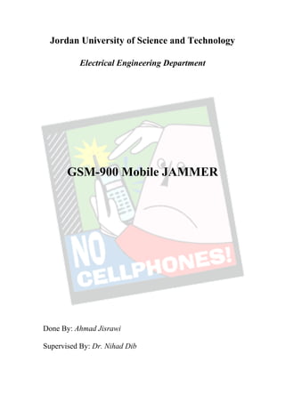
  • 1. Jordan University of Science and Technology Electrical Engineering Department GSM-900 Mobile JAMMER Done By: Ahmad Jisrawi Supervised By: Dr. Nihad Dib
  • 2. 1 Table of Contents Introduction ……………………………………………………………………… 2 Mobile Jamming and Disablers Techniques……………………………………… 3 GSM-Mobile JAMMING Requirements…………………………………………. 7 Design and Implementation of GSM Mobile JAMMER………………………….11 RF-Section ………………………………………………………………..11 Voltage controlled oscillator……………………………………....12 RF-Power Amplifier………………………………………………13 Antenna…………………………………………………………....15 IF-Section………………………………………………………………... 18 Triangular wave generator……………………………………….. 18 Noise Generator…………………………………………………... 20 Signal mixer and DC-offset Circuit………………………………..21 Power Supply………………………………………………………………24 Conclusions………………………………………………………………………...26 References………………………………………………………………………….27
  • 3. 2 INTRODUCTION A GSM Jammer is a device that transmit signal on the same frequency at witch the GSM system operates, the jamming success when the mobile phones in the area where the jammer is located are disabled. Communication jamming devices were first developed and used by military. Where tactical commanders use RF communications to exercise control of their forces, an enemy has interest in those communications. This interest comes from the fundamental area of denying the successful transport of the information from the sender to the receiver. Nowadays the mobile jammer devices are becoming civilian products rather than electronic warfare devices, since with the increasing number of the mobile phone users the need to disable mobile phones in specific places where the ringing of cell phone would be disruptive has increased. These places include worship places, university lecture rooms, libraries, concert halls, meeting rooms, and other places where silence is appreciated. Mosques are example for the places were mobile jammer would be a great solution, although mosques asks politely from prayers to disable their mobile phone during the prayer ,see figure (1), some people forget and the ringing phone of their mobile phone become very annoying specially during the praying time. Figure 1: Typical sign used in places where mobile phone are not allowed
  • 4. 3 Mobile Jamming and Disablers Techniques There are different approaches to prevent mobile phones from ringing in specific area, the main five approaches used or being developed are described in RABC Mobile & Personal Communications Committee’s (M&PCC) meeting of June 22, 1999 [1], these techniques are summarized in this section : 1- Type "A" Device In this device we overpower cell phone's signal with a stronger signal, This type of device comes equipped with several independent oscillators transmitting ‘jamming signals’ capable of blocking frequencies used by paging devices as well as those used by cellular/PCS systems’ control channels for call establishment. When active in a designated area, such devices will (by means of RF interference) prevent all pagers and mobile phones located in that area from receiving and transmitting calls. This type of device transmits only a jamming signal and has very poor frequency selectivity, which leads to interference with a larger amount of communication spectrum than it was originally intended to target. Technologist Jim Mahan said, “There are two types. One is called brute force jamming, which just blocks everything. The problem is, it’s like power-washing the airwaves and it bleeds over into the public broadcast area. The other puts out a small amount of interference, and you could potentially confine it within a single cell block. You could use lots of little pockets of small jamming to keep a facility under control.” 2- Type "B" Device This device also called "Intelligent Cellular Disablers devices", and it does not transmit an interfering signal on the control channels. The device basically works as a detector, and it capable to communicate with the cellular base station. When the
  • 5. 4 device detects the presence of a mobile phone in the "silent" room; a prevention of authorization of call establishment is done by the software at the base station. The device signals the base station that the target user is in a ‘quiet’ room; therefore, do not establish the communication. Messages can be routed to the user’s voice- mail box, if the user subscribes to a voice- mail service. This process of detection and interruption of call establishment is done during the interval normally reserved for signaling and handshaking. This intelligent device as it’s name imply can recognize emergency calls and also can allow specific pre-registered users to use their mobile phones for a specified duration. Although this device sounds the best solution for disabling mobile phone, a provision is needed by the cellular/PCS service providers or provision by a third- party working cooperatively with full support of the cellular/PCS service providers, allowing the detector device to be integral part of the cellular/PCS systems. 3- Type "C" Device This device also called "Intelligent Beacon Disablers ", as in the type "B" device it does not transmit an interfering signal on the control channels. The device, when located in a specific "silent" room, functions as a ‘beacon’ and any compatible terminal is ordered to disable its ringer or disable its operation. In the coverage area of the beacon only terminals which have a compatible receiver would respond and this should be built on a separate technology from cellular/PCS, for example Bluetooth technology. Also the handset must re-enable its normal function as it leaves the coverage area of the beacon. The need for intelligent handsets with a separate receiver for the beacon receiver from the cellular/PCS receiver, make effective deployment for the type "C" device will be problematic for many years.
  • 6. 5 4- Type "D" Device This jammer is similar to type "A" , but with a receiver, so that jammer is predominantly in receive mode and when the device detects the presence of a mobile phone in the "silent" room; it will intelligently choose to interact and block the cell phone by transmitting jamming signal. This jam signal would only stay on as long as the mobile continues to make a link with the base station; otherwise there would be no jamming transmission. Thus this device much less electromagnetic pollution in terms of raw power transmitted and frequency spectrum from the type "A" Jammer, and therefore much less disruptive to passing traffic. This technique could be implemented without cooperation from PCS/cellular providers. Also this technique has an added advantage over Type B in that no added overhead time or effort is spent negotiating with the cellular network. 5- Type "E" Device This technique is using EMI suppression techniques to make a room into what is called a Faraday cage. Although labour intensive to construct, the Faraday cage essentially blocks, or greatly attenuates, virtually all electromagnetic radiation from entering or leaving the cage or in this case a target room. With current advances in EMI shielding techniques and commercially available products one could conceivably implement this into the architecture of newly designed buildings for so-called “quiet-conference” rooms. Emergency calls would be blocked unless there was a way to receive and decode the Emergency Call transmissions, pass by coax outside the room and re- transmitted.
  • 7. 6 This passive configuration is currently legal in most worlds' countries for any commercial or residential location; however some building may not allow this type of construction. Table 1 shows a comparison between the different Jammer/Disablers techniques. Type Emergency call Efficiency Regularity Approval Implementation "A" Blocked Low Not allowed Very simple "B" Allowed Medium Required Complex (Required third party Cellular/PCS Services) "C" Allowed High Required Complex (Required Intelligent Handset) "D" Allowed Medium Required Simple "E" Blocked High(No signal transmitted) Allowed Simple Table 1: Comparison between Jammer/Disabler Techniques
  • 8. 7 GSM-Mobile JAMMING Requirements As discussed in part-2, jamming objective is to inject an interference signal into the communications frequency so that the actual signal is completely submerged by the interference. It is important to notice that transmission can never be totally jammed - jamming hinders the reception at the other end. The problem here for the jammer is that only transmitters can be found using direction finding and the location of the target must be a specific location, usually where the jammer is located and this is because the jamming power is never infinite. Jamming is successful when the jamming signal denies the usability of the communications transmission. In digital communications, the usability is denied when the error rate of the transmission cannot be compensated by error correction. Usually a successful jamming attack requires that the jammer power is roughly equal to signal power at the receiver. The effects of jamming depend on the jamming-to-signal ratio (J/S), modulation scheme, channel coding and interleaving of the target system. Generally Jamming-to-Signal ratio can be measured according to the following Equation. [2] BLRGGP BLRGGP S J jjjrrttrt rrtrrjjrj 2 2 = Where: Pj = jammer power Pt = transmitter power Gjr = antenna gain from jammer to receiver Grj = antenna gain from receiver to Jammer Gtr = antenna gain from transmitter to receiver Grt = antenna gain from receiver to transmitter
  • 9. 8 Br = communications receiver bandwidth Bj = jamming transmitter bandwidth Rtr = range between communications transmitter and receiver Rjt = range between jammer and communications receiver Lj = jammer signal loss (including polarization mismatch) Lr = communication signal loss The above Equation indicates that the jammer Effective Radiated Power, which is the product of antenna gain and output power, should be high if jamming efficiency is required. On the other hand, in order to prevent jamming, the antenna gain toward the communication partner should be as high as possible while the gain towards the jammer should be as small as possible. As the equation shows, the antenna pattern, the relation between the azimuth and the gain, is a very important aspect in jamming. Also as we know from Microwave and shown in the equation distance has a strong influence on the signal loss. If the distance between jammer and receiver is doubled, the jammer has to quadruple its output in order for the jamming to have the same effect. It must also be noted here that jammer path loss is often different from the communications path loss; hence gives jammer an advantage over communication transmitters. In the GSM network, the Base Station Subsystem (BSS) takes care of the radio resources. In addition to Base Transceiver Station (BTS), the actual RF transceiver, BSS consists of three parts. These are the Base Station Controller (BSC), which is in charge of mobility management and signaling on the Air-interface between Mobile Station (MS), the BTS, and the Air-interface between BSS and Mobile Services Switching Center (MSC).
  • 10. 9 The GSM Air-interface uses two different multiplexing schemes: TDMA (Time Division Multiple Access) and FDMA (Frequency Division Multiple Access). The spectrum is divided into 200 kHz channels (FDMA) and each channel is divided into 8 timeslots (TDMA). Each 8 timeslot TDMA frame has duration of 4.6 ms (577 s/timeslot) [3]. The GSM transmission frequencies are presented in Table 2 Uplink Downlink GSM 900 890-915 MHz 935-960 MHz Table 2: GSM 900 Frequency Band Frequency Hopping in GSM is intended for the reduction of fast fading caused by movement of subscribers. The hopping sequence may use up to 64 different frequencies, which is a small number compared to military FH systems designed for avoiding jamming. Also, the speed of GSM hopping is approximately 200 hops / s; So GSM Frequency Hopping does not provide real protection against jamming attacks. Although FH doesn’t help in protection against jamming, interleaving and forward error correction scheme GSM Systems can protect GSM against pulsed jamming. For GSM it was shown that as the specified system SNRmin is 9 dB [3], a jammer requires a 5 dB S/J in order to successfully jam a GSM channel. The optimum GSM SNR is 12 dB, after this point the system starts to degrade. GSM system is capable to withstand abrupt cuts in Traffic Channel (TCH) connections. These cuts are normally caused by propagation losses due to obstacles such as bridges. Usually another cell could be used to hold communication when the original BTS has disconnected. The GSM architecture provides two solutions for this: first handover when the connection is still available, second call re- establishment when the original connection is totally lost. Handover decisions are
  • 11. 10 made based on transmission quality and reception level measurements carried out by the MS and the BTS. In jamming situations call re-establishment is probably the procedure the network will take in order to re-connect the jammed TCH. It is obvious that downlink jamming (i.e. Jamming the mobile station 'handset' receiver) is easier than uplink, as the base station antenna is usually located far a way from the MS on a tower or a high building. This makes it efficient for the jammer to overpower the signal from BS. But the Random Access Channel (RACH) control channels of all BTSs in the area need to be jammed in order to cut off transmission. To cut an existing connections, the jamming has to last at least until the call re- establishment timer at the MSC expires and the connection is released, which means that an existing call can be cut after a few seconds of effective jamming. The GSM RACH random access scheme is very simple: when a request is not answered, the mobile station will repeat it after a random interval. The maximum number of repetitions and the time between them is broadcast regularly. After a MS has tried to request service on RACH and has been rejected, it may try to request service from another cell. Therefore, the cells in the area should be jammed. In most cases, the efficiency of a cellular jamming is very difficult to determine, since it depends on many factors, which leaves the jammer confused.
  • 12. 11 Design and Implementation of GSM Mobile JAMMER The Implementation of type "A" JAMMER is fairly simple, the block diagram for this type is shown in figure (2), it shows the main parts which are: RF-section, IF- section, and the power supply. Figure 2: Block diagram of the mobile Jammer 1-RF-Section: The RF-section is the most important part of the mobile jammer it consist of the Voltage Controlled Oscillator (VCO), RF Power amplifiers, and the antenna. These components were selected according to the desired specification of the jammer such as the frequency range and the coverage range. Its important to note that all the components used has 50 ohm input/output impedance, so 50 ohm microstrip was needed for matching between the components. The width of the microstrip was calculated using the following Equations for w/h >1: [4] To obtain the desired output jamming power for coverage range of 20 m first we found he jamming power required at the mobile receiver "Jr", knowing that SNRmin = 9 dB and Smax = -15dBm (i.e. worst jamming case).[5] then from Power Supply 5, 9,-9 V IF Section RF Section RF jamming signal
  • 13. 12 SNRmin = S/J, where S = the signal power, J = the jamming power Jr = -24dBm, then by invoking the free space path loss equation: [6] F = 32.45 + 20 log(f*D), where "Ds" is distance in Km and "f" is frequency in MHz , for 20 m the loss equals 58 dB hence the jammer should transmit a jamming signal with power equals : 58 dB -24dBm = 34dBm, to sustain a 20m jamming area. 1.1 - Voltage Controlled Oscillator: The VCO is responsible for generating the RF signal which will over power the mobile downlink signal. The selection of the VCO was influenced by two main factors, the frequency of the GSM system, which will be jammed and the availability of the chip. For the first factor which implies that the VCO should cover the frequencies from 935 MHz to 960 MHz, The MAX2623 VCO from MAXIM IC was found to be a good choice, and fortunately the second factor was met sequentially since MAXIM IC was willing to send two of the MAX2623 for free. Figure 3: Maxim2623 typical connection The MAX2623 VCO is implemented as an LC oscillator configuration, integrating all of the tank circuitry on-chip, this makes the VCO extremely easy-
  • 14. 13 to-use, and the tuning input is internally connected to the varactor as shown in figure (3). The typical output power is -3dBm, and the output was best swept over the desired range when the input tuning voltage was around 120 KHz. 1.2 - RF Power Amplifier To achieve the desired output power a gain stages was needed, about searching for a suitable power amplifier I found that its easer and cheaper to look for power amplifier from an old Mobile phones. The PF08103B Hitachi power amplifier module from NOKIA mobile phone was sufficient to amplify an input signal in the range 800MHz to 1GHz by 34 dB. But its recommend in the data sheet that the power at the input should be 1dBm. To meet this requirement I used another power amplifier stage after the VCO and before the Hitachi Power Amplifier module, for this stage I used the MAR-4SM power amplifier from Mini-Circuits Company, the MAR-4SM has a typical gain of 8 dB for the frequencies range from dc to 1 GHz, so the output after this stage should be around 5dBm. A Typical biasing Configuration for the MAR-4SM is shown in figure (4),the bias current is delivered from a voltage supply Vcc (+9V in this design) through the resistor Rbias and the RF choke (inductor). The effect of the resistor is to reduce the effect of device voltage (Vc) variation on the bias current by so simulating a current source. Blocking capacitors are needed at the input and output ports. To prevent stray coupling to other signal processing components we use a bypass capacitor at the connection to the DC supply.
  • 15. 14 Figure 4: Typical biasing Configuration for the MAR-4SM The bias current is given by the following equation: Ibias = (Vcc - Vd) / Rbias The design for the MAR amplifier was carried on a useful program form AGILENT TECHNOLOGIES called APPCAD, the results are shown in figure 5 Figure 5: Biasing MAR-4SM Now the power before the Hitachi RF amplifier is 5dBm and since 1dBm is required; I used 4dB T-Network attenuator as shown in figure (6). [7] The attenuator also designed to have 50 ohm characteristic impedance to easily match the whole circuits.
  • 16. 15 Figure 6: T-Network Attenuator For 4-dB attenuation and symmetric Network S12 = S21 = 0.631 (i.e. VVV 122 *631.0== − ), and for 50 ohm characteristic impedance we found the values of the resistors using the following equations: 50 = (R2 + 50) // (R3) + R1 0.631 = (X / (X + R1))*(50 / (50 + R1)), where X = (R2 + 50)//R3. 1.3 - Antenna The most important part of any transmitter is the antenna, so a suitable antenna should be selected. The antenna used in this project is 1/4 wave monopole antenna, and it has 50 Ohm impedance so that the antenna is matched to the transmission system. Also this antenna has low VSWR less than 1.7, and a bandwidth of 150 MHz around 916 MHz center frequency which cover the mobile jammer frequency range. The antenna gain is 2dBi. The patterns for the antenna are shown below: (a) (b) Figure 7: (a) Monopole Principal E-plane Pattern (b) Monopole Principal H-plane Pattern (Source: www.rfcafe.com)
  • 17. 16 Figure (8) shows the output of the VCO after the two RF amplifiers using the spectrum analyzer, and as shown it is tuned to sweeps from 625 – 960 MHz Figure 8: output of the mobile jammer It is important to note that the RF-Section was implemented on FR-4 printed circuit board (PCB) with thickness of 1/32 inches. Also RF layout issues such as good grounding, transmission lines, and vias was taken into consideration when designing the layout for the RF-Section. Figure (9) shows the finished PCB of the RF-Section. Figure 9: PCB of RF section of the mobile jammer
  • 18. 17 The Circuit Diagram for the RF-section was done using Orcad Capture, and it is shown in figure (10) Figure 10: Circuit diagram for the RF-Section
  • 19. 18 2-IF-Section: The function of the IF-section of the Mobile jammer is to generate the tuning signal for the VCO in The RF-Section, which will sweep the VCO through the desired range of frequencies. This tuning signal is generated by a triangular wave generator along with noise generator, and then offset by proper amount so as to sweep the VCO output from the minimum desired frequency to a maximum. 2.1- Triangular Wage Generator: In the first revision for the mobile jammer I used operational amplifiers as relaxation oscillator to produce square wave generator and another OP-Amp as integrator to produce the desired triangular waveform, but since the gain-bandwidth for most OP-Amp is law the maximum output frequency was around 20 KHz which was not sufficient to sweep the MAXIM-VCO. The solution for this was to use 555- Timer as ASTABLE MULTIVIBRATOR. [8] Figure 11: 555 timer connected as oscillator
  • 20. 19 The 555 timer consists basically of two comparators, a flip-flop, a discharge transistor, and a resistive voltage divider. The resistive divider is used to set the voltage comparator levels all three comparator levels. A 555 timer connected to operate in the astable mode as a free-running nonsinusoidal oscillator (astable multivibrator) is shown in Figure (11). The threshold input is connected to the trigger input. The external components Rl, R2, and Cex form the timing circuit that sets the frequency of oscillation. The 0.01 uF capacitor connected to the control input is strictly for decoupling and has no effect on the operation; in some cases it can be left off. Initially, when the power is turned on, the capacitor Cext is uncharged and thus the trigger voltage (pin 2) is at 0 V. This causes the output of the lower comparator to be high and the output of the upper comparator to be low, forcing the output of the flip-flop, and thus the base of Qd, low and keeping the transistor off. Now, Cext begins charging through R1 & R2 (to obtain 50% duty cycle, one can connect a diode parallel with R2 and choose R2 = R1 ).When the capacitor voltage reaches 1/3VCC, the lower comparator switches to its low output state, and when the capacitor voltage reaches 2/3VCC the upper comparator switches to its high output state. This resets the flip flop causes the base of Qd to go high, and turns on the transistor. This sequence creates a charge path for the capacitor through R2 and the transistor, as indicated. The cap now begins to discharge, causing the upper comparator to go low. At the point whet capacitor discharges down to 1/3VCC, the lower comparator switches high, setting the flip flop, which makes the base of Qd low and turns off the transistor. Another charging cycles begins, and the entire process repeats. The result is a rectangular wave output whose
  • 21. 20 duty cycle depends on the values of R1 and R2. The frequency of oscillation is given by the following formula: ( )CRR f ext r 21 44.1 + = Using the above equation for frequency equal 110 KHz, one can found the values of R1, R2, and Cext. Then the output was taken from the voltage on the external capacitor which has triangular wave form. A simulation was done to verify the operation of circuit and the output is shown in figure (12). Figure 12: The output voltage on C ext To avoid loading the timing circuit and changing the operating frequency, the triangular wave on the terminal of the external capacitor was buffered using OP- Amp. 2.2- Noise Generator: To achieve jamming a noise signal is mixed with the triangle wave signal to produce the tuning voltage for the VCO. The noise will help in masking the jamming transmission, making it look like random "noise" to an outside observer. Without the noise generator, the jamming signal is just a sweeping, unmodulated Continuous Wave RF carrier.
  • 22. 21 The noise generator used in this design is based on the avalanche noise generated by a Zener breakdown phenomenon. It is created when a PN junction is operated in the reverse breakdown mode. The avalanche noise is very similar to shot noise, but much more intense and has a flat frequency spectrum (white). The magnitude of the noise is difficult to predict due to its dependence on the materials. Basically the noise generator circuit consists of a standard 6.8 volt Zener diode with a small reverse current, a transistor buffer, and The National LM386 audio amplifier which acts as a natural band-pass filter and small-signal amplifier. The output spectrum of the noise generator is shown in figure (13) Figure 13: White-noise generator output spectrum (Source: www.maxim-ic.com) 2.3- Signal Mixer and DC-Offset circuits: The triangle wave and noise signals are mixed using Op-Amp configured as summer, see figure (14). Then a DC voltage is added to the resulted signal to obtain the required tuning voltage using Diode-Clamper circuit. Figure (15) shows a diode clamper circuit with Bias. To gain good clamping the RC time
  • 23. 22 constant selected so that it's more than ten times the period of the input frequency, also a potentiometer was added to control the biasing voltage so as to get the desired tuning voltage. Figure 14: OP-Amp Summer Circuit Figure 15: Positive Diode-Clamper with bias The complete schematic for the IF section is shown in figure (16), and the printed circuit board for the IF section is shown below Figure 16: PCB of the IF section for the mobile Jammer
  • 24. 23 Figure 16: The complete schematic for the IF section
  • 25. 24 3- Power Supply The mobile jammer was designed for fixed use, and to take its power from the regular 220V AC wall outlets. The IF & RF sections of the jammer require +5, +9, and -9 DC Voltages. So a dc-dual polarity power supply should be designed. Figure 17: Block diagram of dual polarity power supply The basic parts for a power supply are rectifier, filter, and regulator. The rectifier coverts the ac input voltage to a pulsating dc voltage and can be either half wave rectifier and full wave rectifier, the one we use is the full wave rectifier which has the advantage that it allows unidirectional current to the load during the entire cycle of the input voltage and the result of the full wave rectification is an output voltage with a frequency twice the input frequency that pulsated every half-cycle of the input. The average value for a full wave rectifier for a sinusoidal input is given by: VAVG = 2* VP / π The full wave rectifier used in this project is a full-wave bridge rectifier, which uses four diodes the peak output is given by the: VP = VPsec – 1.4, where VPsec is the output voltage across the secondary winging of the transformer. In the project the transformer used is 220/12, 1.5 A rating, so VAVG = 11 V and VP = 15.88 V. The second part of the power supply is the filter which eliminate the fluctuations in the output of the full wave rectifier so as to produce a constant dc voltage, the filter is Transformer Rectifier Filter + Regulator +5V + Regulator +9V - Regulator - 9V
  • 26. 25 simply a capacitor and its chosen to be as large as possible to minimize voltage ripple in the output. The final part of the power supply is the regulator and it is used to provide the desired constant dc output that is basically independent of the input voltage. Single chip regulators were used to give +5, +9, and -9 dc voltages. Figure 18: Circuit schematic of the power supply Figure 19: PCB of the power supply
  • 27. 26 Conclusion: In this project a GSM-900 Mobile Jammer was designed and built. The project was tested against the two GSM-900 Networks in Jordan (i.e. Fastlink and Mobilecom) and has proven success with average range of 10 m. I faced a problem with tuning the VCO to the desired range, due to power supply variation with load current, so to improve the jammer a more stable power supply should be designed for robust operation of the device, also the power supply was not capable to deliver the needed current for the power amplifier and this the reason for the actual coverage range of the device was not the same as designed for. Testing in different location shows the dependent of the jamming range on the signal strength, for instance in low GSM coverage area the jamming range exceed 20 m. In general the jamming attack was protected by network signal power, and having large power jamming device the GSM network will be jammed for sure, from this observation it can be concluded that the protection against jamming attack in the GSM system was very weak and couldn’t withstand the simplest jamming techniques. The main disadvantage of the mobile jammer is that the transmission of the jamming signal which is prohibited by law in many countries, for instance the fines for this offense can range as high as 11,000 $.Despite the legal issues the transmission of high power signal may affect the operation of some critical devices, such as hearing impairment hardware solution. These disadvantages will constrain the use of mobile jammer.
  • 28. 27 References: [1] Mobile & Personal Communications Committee of the Radio Advisory Board of Canada, “Use of jammer and disabler Devices for blocking PCS, Cellular & Related Services” http://www.rabc.ottawa.on.ca/e/Files/01pub3.pdf [2] Braun, T.; Carle, G.; Koucheryavy, Y.; Tsaoussidis, V., Wired/Wireless Internet Communications, Third International Conference, WWIC 2005, Xanthi, Greece, May 11- 13, 2005, Proceedings, p188. [3] John Scourias, Overview of the Global System for Mobile Communications, http://ccnga.uwaterloo.ca/~jscouria/GSM/gsmreport.html#1 [4] Rick Hartley, RF / Microwave PC Board Design and Layout, www.jlab.org/accel/eecad/pdf/050rfdesign.pdf [5] http://www.mumor.org/public/publications/ISCAS_2004_MuMo_Receiver.pdf [6] Siwiak, K., Radiowave Propagation and Antennas for Personal Communications, Artech House, 2nd.ed, p138. [7] Pozar, D. M., Microwave Engineering, John Wiley and Sons, 2nd.Ed, p198. [8] Gopalan, K. Gopal, Introduction to Digital Microelectronic Circuits, Irwin, New York, 1996. pp. 496-500. [9] Floyd, Electronic Devices, Prentice Hall, 5th. Ed, pp.60-85 [10] Horowitz, P.; Hill, W., the Art of Electronics, 2nd. Ed, Cambridge University Press.