Kotlin Multiplatform & Compose Multiplatform - Starter kit for pragmatics
Fn2969 8255
1. ®
82C55A
Data Sheet November 16, 2006 FN2969.10
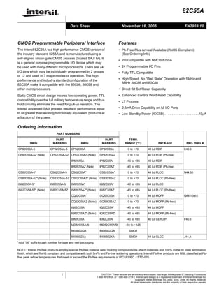
CMOS Programmable Peripheral Interface Features
The Intersil 82C55A is a high performance CMOS version of • Pb-Free Plus Anneal Available (RoHS Compliant)
the industry standard 8255A and is manufactured using a (See Ordering Info)
self-aligned silicon gate CMOS process (Scaled SAJI IV). It
• Pin Compatible with NMOS 8255A
is a general purpose programmable I/O device which may
be used with many different microprocessors. There are 24 • 24 Programmable I/O Pins
I/O pins which may be individually programmed in 2 groups • Fully TTL Compatible
of 12 and used in 3 major modes of operation. The high
performance and industry standard configuration of the • High Speed, No “Wait State” Operation with 5MHz and
8MHz 80C86 and 80C88
82C55A make it compatible with the 80C86, 80C88 and
other microprocessors. • Direct Bit Set/Reset Capability
Static CMOS circuit design insures low operating power. TTL • Enhanced Control Word Read Capability
compatibility over the full military temperature range and bus • L7 Process
hold circuitry eliminate the need for pull-up resistors. The
Intersil advanced SAJI process results in performance equal • 2.5mA Drive Capability on All I/O Ports
to or greater than existing functionally equivalent products at • Low Standby Power (ICCSB) . . . . . . . . . . . . . . . . . . .10μA
a fraction of the power.
Ordering Information
PART NUMBERS
PART PART TEMP.
5MHz MARKING 8MHz MARKING RANGE (°C) PACKAGE PKG. DWG. #
CP82C55A-5 CP82C55A-5 CP82C55A CP82C55A 0 to +70 40 Ld PDIP E40.6
CP82C55A-5Z (Note) CP82C55A-5Z CP82C55AZ (Note) CP82C55AZ 0 to +70 40 Ld PDIP (Pb-free)
IP82C55A IP82C55A -40 to +85 40 Ld PDIP
IP82C55AZ (Note) IP82C55AZ -40 to +85 40 Ld PDIP (Pb-free)
CS82C55A-5* CS82C55A-5 CS82C55A* CS82C55A* 0 to +70 44 Ld PLCC N44.65
CS82C55A-5Z* (Note) CS82C55A-5Z CS82C55AZ* (Note) CS82C55AZ 0 to +70 44 Ld PLCC (Pb-free)
IS82C55A-5* IS82C55A-5 IS82C55A* IS82C55A* -40 to +85 44 Ld PLCC
IS82C55A-5Z* (Note) IS82C55A-5Z IS82C55AZ* (Note) IS82C55AZ -40 to +85 44 Ld PLCC (Pb-free)
CQ82C55A* CQ82C55A* 0 to +70 44 Ld MQFP Q44.10x10
CQ82C55AZ (Note) CQ82C55AZ 0 to +70 44 Ld MQFP (Pb-free)
IQ82C55A* IQ82C55A* -40 to +85 44 Ld MQFP
IQ82C55AZ* (Note) IQ82C55AZ -40 to +85 44 Ld MQFP (Pb-free)
ID82C55A ID82C55A -40 to +85 40 Ld CERDIP F40.6
MD82C55A/B MD82C55A/B -55 to +125
8406602QA 8406602QA SMD#
8406602XA 8406602XA SMD# 44 Ld CLCC J44.A
*Add “96” suffix to part number for tape and reel packaging.
NOTE: Intersil Pb-free products employ special Pb-free material sets; molding compounds/die attach materials and 100% matte tin plate termination
finish, which are RoHS compliant and compatible with both SnPb and Pb-free soldering operations. Intersil Pb-free products are MSL classified at Pb-
free peak reflow temperatures that meet or exceed the Pb-free requirements of IPC/JEDEC J STD-020.
1 CAUTION: These devices are sensitive to electrostatic discharge; follow proper IC Handling Procedures.
1-888-INTERSIL or 1-888-468-3774 | Intersil (and design) is a registered trademark of Intersil Americas Inc.
Copyright Intersil Americas Inc. 2002, 2005, 2006. All Rights Reserved
All other trademarks mentioned are the property of their respective owners.
3. 82C55A
Pin Description
SYMBOL TYPE DESCRIPTION
VCC VCC: The +5V power supply pin. A 0.1μF capacitor between VCC and GND is recommended for decoupling.
GND GROUND
D0-D7 I/O DATA BUS: The Data Bus lines are bidirectional three-state pins connected to the system data bus.
RESET I RESET: A high on this input clears the control register and all ports (A, B, C) are set to the input mode with the “Bus
Hold” circuitry turned on.
CS I CHIP SELECT: Chip select is an active low input used to enable the 82C55A onto the Data Bus for CPU
communications.
RD I READ: Read is an active low input control signal used by the CPU to read status information or data via the data bus.
WR I WRITE: Write is an active low input control signal used by the CPU to load control words and data into the 82C55A.
A0-A1 I ADDRESS: These input signals, in conjunction with the RD and WR inputs, control the selection of one of the three
ports or the control word register. A0 and A1 are normally connected to the least significant bits of the Address Bus
A0, A1.
PA0-PA7 I/O PORT A: 8-bit input and output port. Both bus hold high and bus hold low circuitry are present on this port.
PB0-PB7 I/O PORT B: 8-bit input and output port. Bus hold high circuitry is present on this port.
PC0-PC7 I/O PORT C: 8-bit input and output port. Bus hold circuitry is present on this port.
Functional Diagram
+5V GROUP A I/O
POWER PA7-PA0
SUPPLIES PORT A
GND GROUP A (8)
CONTROL
GROUP A
PORT C I/O
BIDIRECTIONAL PC7-PC4
UPPER
DATA BUS (4)
DATA BUS
D7-D0 BUFFER
8-BIT GROUP B
PORT C I/O
INTERNAL
PC3-PC0
DATA BUS LOWER
(4)
RD
READ
WR WRITE GROUP B
CONTROL CONTROL GROUP B I/O
A1
LOGIC PORT B PB7-PB0
A0 (8)
RESET
CS
3 FN2969.10
November 16, 2006
4. 82C55A
Functional Description I/O
PA7-
Data Bus Buffer POWER +5V GROUP A PA0
SUPPLIES GND GROUP A PORT A
This three-state bidirectional 8-bit buffer is used to interface CONTROL (8)
the 82C55A to the system data bus. Data is transmitted or I/O
PC7-
received by the buffer upon execution of input or output GROUP A PC4
BIDIRECTIONAL PORT C
instructions by the CPU. Control words and status DATA BUS UPPER
(4) I/O
information are also transferred through the data bus buffer. DATA PC3-
D7-D0 BUS GROUP B PC0
Read/Write and Control Logic BUFFER 8-BIT PORT C
INTERNAL LOWER
DATA BUS (4)
The function of this block is to manage all of the internal and
external transfers of both Data and Control or Status words. RD I/O
WR READ PB7-
It accepts inputs from the CPU Address and Control busses WRITE
GROUP B PB0
A1 CONTROL GROUP B
and in turn, issues commands to both of the Control Groups. CONTROL PORT B
A0 LOGIC (8)
RESET
(CS) Chip Select. A “low” on this input pin enables the
communication between the 82C55A and the CPU.
(RD) Read. A “low” on this input pin enables 82C55A to send CS
the data or status information to the CPU on the data bus. In FIGURE 1. 82C55A BLOCK DIAGRAM. DATA BUS BUFFER,
essence, it allows the CPU to “read from” the 82C55A. READ/WRITE, GROUP A & B CONTROL LOGIC
FUNCTIONS
(WR) Write. A “low” on this input pin enables the CPU to
write data or control words into the 82C55A. Group A and Group B Controls
The functional configuration of each port is programmed by
(A0 and A1) Port Select 0 and Port Select 1. These input
the systems software. In essence, the CPU “outputs” a
signals, in conjunction with the RD and WR inputs, control
control word to the 82C55A. The control word contains
the selection of one of the three ports or the control word
information such as “mode”, “bit set”, “bit reset”, etc., that
register. They are normally connected to the least significant
initializes the functional configuration of the 82C55A.
bits of the address bus (A0 and A1).
Each of the Control blocks (Group A and Group B) accepts
82C55A BASIC OPERATION
“commands” from the Read/Write Control logic, receives
INPUT OPERATION “control words” from the internal data bus and issues the
A1 A0 RD WR CS (READ)
proper commands to its associated ports.
0 0 0 1 0 Port A → Data Bus
Control Group A - Port A and Port C upper (C7 - C4)
0 1 0 1 0 Port B → Data Bus
Control Group B - Port B and Port C lower (C3 - C0)
1 0 0 1 0 Port C → Data Bus
The control word register can be both written and read as
1 1 0 1 0 Control Word → Data Bus
shown in the “Basic Operation” table. Figure 4 shows the
OUTPUT OPERATION control word format for both Read and Write operations.
(WRITE)
When the control word is read, bit D7 will always be a logic
0 0 1 0 0 Data Bus → Port A “1”, as this implies control word mode information.
0 1 1 0 0 Data Bus → Port B Ports A, B, and C
1 0 1 0 0 Data Bus → Port C The 82C55A contains three 8-bit ports (A, B, and C). All can
1 1 1 0 0 Data Bus → Control be configured to a wide variety of functional characteristics
by the system software but each has its own special features
DISABLE FUNCTION
or “personality” to further enhance the power and flexibility of
X X X X 1 Data Bus → Three-State the 82C55A.
X X 1 1 0 Data Bus → Three-State Port A One 8-bit data output latch/buffer and one 8-bit data
input latch. Both “pull-up” and “pull-down” bus-hold devices
(RESET) Reset. A “high” on this input initializes the control are present on Port A. See Figure 2A.
register to 9Bh and all ports (A, B, C) are set to the input
Port B One 8-bit data input/output latch/buffer and one 8-bit
mode. “Bus hold” devices internal to the 82C55A will hold
data input buffer. See Figure 2B.
the I/O port inputs to a logic “1” state with a maximum hold
current of 400μA. Port C One 8-bit data output latch/buffer and one 8-bit data
input buffer (no latch for input). This port can be divided into
4 FN2969.10
November 16, 2006
5. 82C55A
two 4-bit ports under the mode control. Each 4-bit port
ADDRESS BUS
contains a 4-bit latch and it can be used for the control signal
output and status signal inputs in conjunction with ports A CONTROL BUS
and B. See Figure 2B.
DATA BUS
INPUT MODE
MASTER
RESET
OR MODE RD, WR D7-D0 A0-A1
CHANGE CS
82C55A
INTERNAL EXTERNAL
DATA IN PORT A PIN MODE 0 C
B A
INTERNAL
DATA OUT
(LATCHED) 8 I/O 4 I/O 4 I/O 8 I/O
OUTPUT MODE
PB7-PB0 PC3-PC0 PC7-PC4 PA7-PA0
FIGURE 2A. PORT A BUS-HOLD CONFIGURATION
MODE 1 C
B A
VCC
RESET
OR MODE 8 I/O 8 I/O
CHANGE P
PB7-PB0 CONTROL CONTROL PA7-PA0
OR I/O OR I/O
MODE 2 C
B A
INTERNAL EXTERNAL
DATA IN PORT B, C BI-
8 I/O DIRECTIONAL
PIN
INTERNAL
DATA OUT PB7-PB0 PA7-PA0
(LATCHED) CONTROL
OUTPUT MODE
FIGURE 3. BASIC MODE DEFINITIONS AND BUS INTERFACE
FIGURE 2B. PORT B AND C BUS-HOLD CONFIGURATION
FIGURE 2. BUS-HOLD CONFIGURATION
CONTROL WORD
Operational Description D7 D6 D5 D4 D3 D2 D1 D0
GROUP B
Mode Selection
There are three basic modes of operation than can be PORT C (LOWER)
1 = INPUT
selected by the system software: 0 = OUTPUT
Mode 0 - Basic Input/Output PORT B
1 = INPUT
Mode 1 - Strobed Input/Output 0 = OUTPUT
Mode 2 - Bidirectional Bus MODE SELECTION
0 = MODE 0
When the reset input goes “high”, all ports will be set to the 1 = MODE 1
input mode with all 24 port lines held at a logic “one” level by
internal bus hold devices. After the reset is removed, the GROUP A
82C55A can remain in the input mode with no additional PORT C (UPPER)
initialization required. This eliminates the need to pull-up or 1 = INPUT
0 = OUTPUT
pull-down resistors in all-CMOS designs. The control word
PORT A
register will contain 9Bh. During the execution of the system 1 = INPUT
program, any of the other modes may be selected using a 0 = OUTPUT
single output instruction. This allows a single 82C55A to MODE SELECTION
00 = MODE 0
service a variety of peripheral devices with a simple software 01 = MODE 1
1X = MODE 2
maintenance routine. Any port programmed as an output
port is initialized to all zeros when the control word is written.
MODE SET FLAG
1 = ACTIVE
FIGURE 4. MODE DEFINITION FORMAT
5 FN2969.10
November 16, 2006
6. 82C55A
The modes for Port A and Port B can be separately defined, This function allows the programmer to enable or disable a
while Port C is divided into two portions as required by the CPU interrupt by a specific I/O device without affecting any
Port A and Port B definitions. All of the output registers, other device in the interrupt structure.
including the status flip-flops, will be reset whenever the
INTE Flip-Flop Definition
mode is changed. Modes may be combined so that their
functional definition can be “tailored” to almost any I/O (BIT-SET)-INTE is SET - Interrupt Enable
structure. For instance: Group B can be programmed in (BIT-RESET)-INTE is Reset - Interrupt Disable
Mode 0 to monitor simple switch closings or display
computational results, Group A could be programmed in NOTE: All Mask flip-flops are automatically reset during mode
selection and device Reset.
Mode 1 to monitor a keyboard or tape reader on an interrupt-
driven basis. Operating Modes
The mode definitions and possible mode combinations may Mode 0 (Basic Input/Output). This functional configuration
seem confusing at first, but after a cursory review of the provides simple input and output operations for each of the
complete device operation a simple, logical I/O approach will three ports. No handshaking is required, data is simply
surface. The design of the 82C55A has taken into account written to or read from a specific port.
things such as efficient PC board layout, control signal
Mode 0 Basic Functional Definitions:
definition vs. PC layout and complete functional flexibility to
support almost any peripheral device with no external logic. • Two 8-bit ports and two 4-bit ports
Such design represents the maximum use of the available
• Any Port can be input or output
pins.
• Outputs are latched
Single Bit Set/Reset Feature (Figure 5)
• Inputs are not latched
Any of the eight bits of Port C can be Set or Reset using a
single Output instruction. This feature reduces software • 16 different Input/Output configurations possible
requirements in control-based applications.
When Port C is being used as status/control for Port A or B, MODE 0 PORT DEFINITION
these bits can be set or reset by using the Bit Set/Reset A B GROUP A GROUP B
operation just as if they were output ports.
PORT C PORT C
D4 D3 D1 D0 PORT A (Upper) # PORT B (Lower)
CONTROL WORD
0 0 0 0 Output Output 0 Output Output
D7 D6 D5 D4 D3 D2 D1 D0
0 0 0 1 Output Output 1 Output Input
BIT SET/RESET
X X X 1 = SET 0 0 1 0 Output Output 2 Input Output
0 = RESET
DON’T
CARE 0 0 1 1 Output Output 3 Input Input
BIT SELECT
0 1 0 0 Output Input 4 Output Output
0 1 2 3 4 5 6 7
0 1 0 1 0 1 0 1 B0 0 1 0 1 Output Input 5 Output Input
0 0 1 1 0 0 1 1 B1
0 0 0 0 1 1 1 1 B2 0 1 1 0 Output Input 6 Input Output
0 1 1 1 Output Input 7 Input Input
BIT SET/RESET FLAG 1 0 0 0 Input Output 8 Output Output
0 = ACTIVE
1 0 0 1 Input Output 9 Output Input
FIGURE 5. BIT SET/RESET FORMAT 1 0 1 0 Input Output 10 Input Output
1 0 1 1 Input Output 11 Input Input
Interrupt Control Functions
1 1 0 0 Input Input 12 Output Output
When the 82C55A is programmed to operate in mode 1 or
mode 2, control signals are provided that can be used as 1 1 0 1 Input Input 13 Output Input
interrupt request inputs to the CPU. The interrupt request 1 1 1 0 Input Input 14 Input Output
signals, generated from port C, can be inhibited or enabled
1 1 1 1 Input Input 15 Input Input
by setting or resetting the associated INTE flip-flop, using
the bit set/reset function of port C.
6 FN2969.10
November 16, 2006
7. 82C55A
Mode 0 (Basic Input)
tRR
RD
tIR tHR
INPUT
tAR tRA
CS, A1, A0
D7-D0
tRD tDF
Mode 0 (Basic Output)
tWW
WR
tWD
tDW
D7-D0
tAW tWA
CS, A1, A0
OUTPUT
tWB
Mode 0 Configurations
CONTROL WORD #0 CONTROL WORD #2
D7 D6 D5 D4 D3 D2 D1 D0 D7 D6 D5 D4 D3 D2 D1 D0
1 0 0 0 0 0 0 0 1 0 0 0 0 0 1 0
8 8
A PA7 - PA0 A PA7 - PA0
82C55A 82C55A
4 4
PC7 - PC4 PC7 - PC4
D7 - D0 C D7 - D0 C
4 4
PC3 - PC0 PC3 - PC0
8 8
B PB7 - PB0 B PB7 - PB0
CONTROL WORD #1 CONTROL WORD #3
D7 D6 D5 D4 D3 D2 D1 D0 D7 D6 D5 D4 D3 D2 D1 D0
1 0 0 0 0 0 0 1 1 0 0 0 0 0 1 1
8 8
A PA7 - PA0 A PA7 - PA0
82C55A 82C55A
4 4
PC7 - PC4 PC7 - PC4
D7 - D0 C D7 - D0 C
4 4
PC3 - PC0 PC3 - PC0
8 8
B PB7 - PB0 B PB7 - PB0
7 FN2969.10
November 16, 2006
8. 82C55A
Mode 0 Configurations (Continued)
CONTROL WORD #4 CONTROL WORD #8
D7 D6 D5 D4 D3 D2 D1 D0 D7 D6 D5 D4 D3 D2 D1 D0
1 0 0 0 1 0 0 0 1 0 0 1 0 0 0 0
8 8
A PA7 - PA0 A PA7 - PA0
82C55A 82C55A
4 4
PC7 - PC4 PC7 - PC4
D7 - D0 C D7 - D0 C
4 4
PC3 - PC0 PC3 - PC0
8 8
B PB7 - PB0 B PB7 - PB0
CONTROL WORD #5 CONTROL WORD #9
D7 D6 D5 D4 D3 D2 D1 D0 D7 D6 D5 D4 D3 D2 D1 D0
1 0 0 0 1 0 0 1 1 0 0 1 0 0 0 1
8 8
A PA7 - PA0 A PA7 - PA0
82C55A 82C55A
4 4
PC7 - PC4 PC7 - PC4
D7 - D0 C D7 - D0 C
4 4
PC3 - PC0 PC3 - PC0
8 8
B PB7 - PB0 B PB7 - PB0
CONTROL WORD #6 CONTROL WORD #10
D7 D6 D5 D4 D3 D2 D1 D0 D7 D6 D5 D4 D3 D2 D1 D0
1 0 0 0 1 0 1 0 1 0 0 1 0 0 1 0
8 8
A PA7 - PA0 A PA7 - PA0
82C55A 82C55A
4 4
PC7 - PC4 PC7 - PC4
D7 - D0 C D7 - D0 C
4 4
PC3 - PC0 PC3 - PC0
8 8
B PB7 - PB0 B PB7 - PB0
CONTROL WORD #7 CONTROL WORD #11
D7 D6 D5 D4 D3 D2 D1 D0 D7 D6 D5 D4 D3 D2 D1 D0
1 0 0 0 1 0 1 1 1 0 0 1 0 0 1 1
8 8
A PA7 - PA0 A PA7 - PA0
82C55A 82C55A
4 4
PC7 - PC4 PC7 - PC4
D7 - D0 C D7 - D0 C
4 4
PC3 - PC0 PC3 - PC0
8 8
B PB7 - PB0 B PB7 - PB0
8 FN2969.10
November 16, 2006
9. 82C55A
Mode 0 Configurations (Continued)
CONTROL WORD #12 CONTROL WORD #14
D7 D6 D5 D4 D3 D2 D1 D0 D7 D6 D5 D4 D3 D2 D1 D0
1 0 0 1 1 0 0 0 1 0 0 1 1 0 1 0
8 8
A PA7 - PA0 A PA7 - PA0
82C55A 82C55A
4 4
PC7 - PC4 PC7 - PC4
D7 - D0 C D7 - D0 C
4 4
PC3 - PC0 PC3 - PC0
8 8
B PB7 - PB0 B PB7 - PB0
CONTROL WORD #13 CONTROL WORD #15
D7 D6 D5 D4 D3 D2 D1 D0 D7 D6 D5 D4 D3 D2 D1 D0
1 0 0 1 1 0 0 1 1 0 0 1 1 0 1 1
8 8
A PA7 - PA0 A PA7 - PA0
82C55A 82C55A
4 4
PC7 - PC4 PC7 - PC4
D7 - D0 C D7 - D0 C
4 4
PC3 - PC0 PC3 - PC0
8 8
B PB7 - PB0 B PB7 - PB0
Operating Modes
MODE 1 (PORT A)
Mode 1 - (Strobed Input/Output). This functional
configuration provides a means for transferring I/O data to or PA7-PA0 8
CONTROL WORD
from a specified port in conjunction with strobes or “hand D7 D6 D5 D4 D3 D2 D1 D0 INTE STBA
PC4
shaking” signals. In mode 1, port A and port B use the lines A
1 0 1 1 1/0
on port C to generate or accept these “hand shaking” PC5 IBFA
PC6, PC7
signals. 1 = INPUT
0 = OUTPUT
Mode 1 Basic Function Definitions: PC3 INTRA
• Two Groups (Group A and Group B) RD 2
PC6, PC7 I/O
• Each group contains one 8-bit port and one 4-bit
control/data port
MODE 1 (PORT B)
• The 8-bit data port can be either input or output. Both
inputs and outputs are latched. PB7-PB0 8
CONTROL WORD
• The 4-bit port is used for control and status of the 8-bit port. D7 D6 D5 D4 D3 D2 D1 D0 INTE PC2
B STBB
1 1 1
Input Control Signal Definition PC1 IBFB
(Figures 6 and 7)
STB (Strobe Input) PC0 INTRB
A “low” on this input loads data into the input latch. RD
IBF (Input Buffer Full F/F)
A “high” on this output indicates that the data has been FIGURE 6. MODE 1 INPUT
loaded into the input latch: in essence, an acknowledgment.
IBF is set by STB input being low and is reset by the rising
edge of the RD input.
9 FN2969.10
November 16, 2006
10. 82C55A
tST
STB
tSIB
IBF
tSIT tRIB
INTR
tRIT
RD
tPH
INPUT FROM
PERIPHERAL
tPS
FIGURE 7. MODE 1 (STROBED INPUT)
INTR (Interrupt Request) INTE A
A “high” on this output can be used to interrupt the CPU Controlled by Bit Set/Reset of PC6.
when an input device is requesting service. INTR is set by
INTE B
the condition: STB is a “one”, IBF is a “one” and INTE is a
“one”. It is reset by the falling edge of RD. This procedure Controlled by Bit Set/Reset of PC2.
allows an input device to request service from the CPU by NOTE:
simply strobing its data into the port. 1. To strobe data into the peripheral device, the user must operate
the strobe line in a hand shaking mode. The user needs to send
INTE A OBF to the peripheral device, generates an ACK from the
Controlled by bit set/reset of PC4. peripheral device and then latch data into the peripheral device
on the rising edge of OBF.
INTE B
Controlled by bit set/reset of PC2. MODE 1 (PORT A)
Output Control Signal Definition PA7-PA0 8
CONTROL WORD
(Figure 8 and 9) D7 D6 D5 D4 D3 D2 D1 D0
PC7 OBFA
OBF - (Output Buffer Full F/F). The OBF output will go “low” 1 0 1 1 1/0
INTE PC6 ACKA
to indicate that the CPU has written data out to the specified PC4, PC5 A
port. This does not mean valid data is sent out of the port at 1 = INPUT
0 = OUTPUT
this time since OBF can go true before data is available. INTRA
PC3
Data is guaranteed valid at the rising edge of OBF, (See
WR 2
Note 1). The OBF F/F will be set by the rising edge of the PC4, PC5
WR input and reset by ACK input being low.
ACK - (Acknowledge Input). A “low” on this input informs the
82C55A that the data from Port A or Port B is ready to be MODE 1 (PORT B)
accepted. In essence, a response from the peripheral device PB7-PB0 8
CONTROL WORD
indicating that it is ready to accept data, (See Note 1).
D7 D6 D5 D4 D3 D2 D1 D0
PC1 OBFB
INTR - (Interrupt Request). A “high” on this output can be 1 1 0
used to interrupt the CPU when an output device has INTE PC2 ACKB
B
accepted data transmitted by the CPU. INTR is set when
ACK is a “one”, OBF is a “one” and INTE is a “one”. It is reset
by the falling edge of WR. PC0 INTRB
WR
FIGURE 8. MODE 1 OUTPUT
10 FN2969.10
November 16, 2006
11. 82C55A
tWOB
WR
tAOB
OBF
INTR tWIT
ACK
tAK tAIT
OUTPUT
tWB
FIGURE 9. MODE 1 (STROBED OUTPUT)
PA7-PA0 8 PA7-PA0 8
RD PC4 STBA WR PC7 OBFA
CONTROL WORD CONTROL WORD
PC5 IIBFA PC6 ACKA
D7 D6 D5 D4 D3 D2 D1 D0 D7 D6 D5 D4 D3 D2 D1 D0
1 0 1 1 1/0 1 0 PC3 INTRA 1 0 1 0 1/0 1 1 PC3 INTRA
2 2
PC6, PC7 PC6, PC7 I/O PC4, PC5 PC4, PC5 I/O
1 = INPUT 1 = INPUT
0 = OUTPUT PB7, PB0 8 0 = OUTPUT PB7, PB0 8
WR PC1 OBFB RD PC2 STBB
PC2 ACKB PC1 IBFB
PC0 INTRB PC0 INTRB
PORT A - (STROBED INPUT) PORT A - (STROBED OUTPUT)
PORT B - (STROBED OUTPUT) PORT B - (STROBED INPUT)
Combinations of Mode 1: Port A and Port B can be individually defined as input or output in Mode 1 to support a wide variety of strobed I/O applications.
FIGURE 10. COMBINATIONS OF MODE 1
Operating Modes Output Operations
OBF - (Output Buffer Full). The OBF output will go “low” to
Mode 2 (Strobed Bidirectional Bus I/O)
indicate that the CPU has written data out to port A.
This functional configuration provides a means for
communicating with a peripheral device or structure on a ACK - (Acknowledge). A “low” on this input enables the three-
single 8-bit bus for both transmitting and receiving data state output buffer of port A to send out the data. Otherwise,
(bidirectional bus I/O). “Hand shaking” signals are provided to the output buffer will be in the high impedance state.
maintain proper bus flow discipline similar to Mode 1. Interrupt INTE 1 - (The INTE flip-flop associated with OBF).
generation and enable/disable functions are also available. Controlled by bit set/reset of PC4.
Mode 2 Basic Functional Definitions:
Input Operations
• Used in Group A only STB - (Strobe Input). A “low” on this input loads data into the
• One 8-bit, bidirectional bus Port (Port A) and a 5-bit input latch.
control Port (Port C)
IBF - (Input Buffer Full F/F). A “high” on this output indicates
• Both inputs and outputs are latched
that data has been loaded into the input latch.
• The 5-bit control port (Port C) is used for control and
status for the 8-bit, bidirectional bus port (Port A) INTE 2 - (The INTE flip-flop associated with IBF). Controlled
by bit set/reset of PC4.
Bidirectional Bus I/O Control Signal Definition
(Figures 11, 12, 13, 14)
INTR - (Interrupt Request). A high on this output can be
used to interrupt the CPU for both input or output operations.
11 FN2969.10
November 16, 2006
12. 82C55A
CONTROL WORD
D7 D6 D5 D4 D3 D2 D1 D0
PC3 INTRA
1 1 1/0 1/0 1/0
PA7-PA0 8
PC7 OBFA
INTE PC6
PC2-PC0 1 ACKA
1 = INPUT
0 = OUTPUT
INTE
PORT B 2 PC4 STBA
1 = INPUT
0 = OUTPUT PC5 IBFA
WR
GROUP B MODE
0 = MODE 0
1 = MODE 1 3
PC2-PC0 I/O
RD
FIGURE 11. MODE CONTROL WORD FIGURE 12. MODE 2
DATA FROM
CPU TO 82C55A
WR
tAOB
OBF
tWOB
INTR
tAK
ACK
tST
STB
tSIB
IBF
tAD
tKD
tPS
PERIPHERAL
BUS
tPH tRIB
RD DATA FROM DATA FROM
PERIPHERAL TO 82C55A 82C55A TO PERIPHERAL
DATA FROM
82C55A TO CPU
NOTE: Any sequence where WR occurs before ACK and STB occurs before RD is permissible. (INTR = IBF • MASK • STB • RD + OBF • MASK
• ACK • WR)
FIGURE 13. MODE 2 (BIDIRECTIONAL)
12 FN2969.10
November 16, 2006
14. 82C55A
MODE DEFINITION SUMMARY
MODE 0 MODE 1 MODE 2
IN OUT IN OUT GROUP A ONLY
PA0 In Out In Out
PA1 In Out In Out
PA2 In Out In Out
PA3 In Out In Out
PA4 In Out In Out
PA5 In Out In Out
PA6 In Out In Out
PA7 In Out In Out
PB0 In Out In Out
PB1 In Out In Out
PB2 In Out In Out
Mode 0
PB3 In Out In Out or Mode 1
PB4 In Out In Out Only
PB5 In Out In Out
PB6 In Out In Out
PB7 In Out In Out
PC0 In Out INTRB INTRB I/O
PC1 In Out IBFB OBFB I/O
PC2 In Out STBB ACKB I/O
PC3 In Out INTRA INTRA INTRA
PC4 In Out STBA I/O STBA
PC5 In Out IBFA I/O IBFA
PC6 In Out I/O ACKA ACKA
PC7 In Out I/O OBFA OBFA
Special Mode Combination Considerations INPUT CONFIGURATION
There are several combinations of modes possible. For any D7 D6 D5 D4 D3 D2 D1 D0
combination, some or all of Port C lines are used for control
I/O I/O IBFA INTEA INTRA INTEB IBFB INTRB
or status. The remaining bits are either inputs or outputs as
defined by a “Set Mode” command. GROUP A GROUP B
During a read of Port C, the state of all the Port C lines, OUTPUT CONFIGURATION
except the ACK and STB lines, will be placed on the data D7 D6 D5 D4 D3 D2 D1 D0
bus. In place of the ACK and STB line states, flag status will
appear on the data bus in the PC2, PC4, and PC6 bit OBFA INTEA I/O I/O INTRA INTEB OBFB INTRB
positions as illustrated by Figure 17.
GROUP A GROUP B
Through a “Write Port C” command, only the Port C pins FIGURE 15. MODE 1 STATUS WORD FORMAT
programmed as outputs in a Mode 0 group can be written.
No other pins can be affected by a “Write Port C” command, D7 D6 D5 D4 D3 D2 D1 D0
nor can the interrupt enable flags be accessed. To write to
OBFA INTE1 IBFA INTE2 INTRA X X X
any Port C output programmed as an output in Mode 1
group or to change an interrupt enable flag, the “Set/Reset GROUP A GROUP B
Port C Bit” command must be used. (Defined by Mode 0 or Mode 1 Selection)
With a “Set/Reset Port C Bit” command, any Port C line FIGURE 16. MODE 2 STATUS WORD FORMAT
programmed as an output (including IBF and OBF) can be
written, or an interrupt enable flag can be either set or reset. Current Drive Capability
Port C lines programmed as inputs, including ACK and STB Any output on Port A, B or C can sink or source 2.5mA. This
lines, associated with Port C are not affected by a “Set/Reset feature allows the 82C55A to directly drive Darlington type
Port C Bit” command. Writing to the corresponding Port C bit drivers and high-voltage displays that require such sink or
positions of the ACK and STB lines with the “Set Reset Port source current.
C Bit” command will affect the Group A and Group B
interrupt enable flags, as illustrated in Figure 17. Reading Port C Status (Figures 15 and 16)
In Mode 0, Port C transfers data to or from the peripheral
device. When the 82C55A is programmed to function in
14 FN2969.10
November 16, 2006
15. 82C55A
Modes 1 or 2, Port C generates or accepts “hand shaking” Applications of the 82C55A
signals with the peripheral device. Reading the contents of
The 82C55A is a very powerful tool for interfacing peripheral
Port C allows the programmer to test or verify the “status” of
equipment to the microcomputer system. It represents the
each peripheral device and change the program flow
optimum use of available pins and is flexible enough to
accordingly.
interface almost any I/O device without the need for
There is not a special instruction to read the status additional external logic.
information from Port C. A normal read operation of Port C is
Each peripheral device in a microcomputer system usually
executed to perform this function.
has a “service routine” associated with it. The routine
manages the software interface between the device and the
INTERRUPT ALTERNATE PORT C CPU. The functional definition of the 82C55A is programmed
ENABLE FLAG POSITION PIN SIGNAL (MODE) by the I/O service routine and becomes an extension of the
INTE B PC2 ACKB (Output Mode 1) system software. By examining the I/O devices interface
or STBB (Input Mode 1) characteristics for both data transfer and timing, and
INTE A2 PC4 STBA (Input Mode 1 or Mode matching this information to the examples and tables in the
2) detailed operational description, a control word can easily be
INTE A1 PC6 ACKA (Output Mode 1 or
developed to initialize the 82C55A to exactly “fit” the
Mode 2) application. Figures 18 through 24 present a few examples
of typical applications of the 82C55A.
FIGURE 17. INTERRUPT ENABLE FLAGS IN MODES 1 AND 2
INTERRUPT
REQUEST
PC3 PA0
PA1 HIGH SPEED
PA2 PRINTER
PA3
PA4
PA5
MODE 1
PA6
(OUTPUT)
PA7 HAMMER
RELAYS
PC7 DATA READY
PC6 ACK
PC5 PAPER FEED
PC4 FORWARD/REV.
82C55A
PB0
PB1
PB2
PB3
PB4
MODE 1 PB5 PAPER FEED
(OUTPUT) PB6 FORWARD/REV.
PB7 RIBBON
CARRIAGE SEN.
PC1 DATA READY
PC2 ACK
PC0
INTERRUPT CONTROL LOGIC
REQUEST AND DRIVERS
FIGURE 18. PRINTER INTERFACE
15 FN2969.10
November 16, 2006