SlideShare a Scribd company logo
1 of 91
Download to read offline
ELH: 1.3 PIC & ARM MICROCONTROLLER UNIT – II
1
Notes by Mr. Chandrakantha T S, Dept.t of PG Studies & Research in Electronics Kuvempu University, Jnanasahyadri, Shankaraghatta,2023-24
ARM (Acorn RISC Machine) Processor
Introduction to ARM Processor
 The ARM (Acorn RISC Machine) processor is a family of Reduced Instruction Set
Computing (RISC) architectures designed for embedded systems and other specialized
applications.
 Renowned for its power efficiency, performance, and versatility, ARM processors have
become a dominant force in the world of computing, particularly in the realm of
embedded systems.
Brief History
 Formation and Early Years:
 The British computer manufacturer Acorn Computers first developed the Acorn
RISC Machine architecture (ARM) in the 1980s to use in its personal
computers.
 The first ARM architecture, ARM1, was released in 1985 as a 32-bit RISC
processor.
ELH: 1.3 PIC & ARM MICROCONTROLLER UNIT – II
2
Notes by Mr. Chandrakantha T S, Dept.t of PG Studies & Research in Electronics Kuvempu University, Jnanasahyadri, Shankaraghatta,2023-24
 Evolution and Partnerships:
 In 1990, ARM Ltd. was founded as a joint venture between Acorn, Apple, and
VLSI Technology.
 The ARM architecture continued to evolve, with subsequent versions offering
enhanced performance and features.
 Widespread Adoption:
 ARM gained significant traction in the 1990s and 2000s, becoming the
architecture of choice for many mobile devices, including smartphones and
tablets.
 Business Model:
 ARM operates on a licensing model, allowing other companies to use its
architecture in their designs. This approach has contributed to the widespread
adoption of ARM processors across various industries.
 Acquisition by SoftBank:
 In 2016, SoftBank Group acquired ARM Holdings, marking a significant
development in the history of the company.
ARM Core:
 Definition:
 The term "ARM core" refers to the central processing unit (CPU) design based
on ARM architecture. ARM cores are the fundamental building blocks of ARM
processors.
 It's important to note that ARM, as a company, specializes in designing and
licensing intellectual property (IP) rather than manufacturing silicon.
ELH: 1.3 PIC & ARM MICROCONTROLLER UNIT – II
3
Notes by Mr. Chandrakantha T S, Dept.t of PG Studies & Research in Electronics Kuvempu University, Jnanasahyadri, Shankaraghatta,2023-24
 ARM follows a licensing model where it designs CPU architectures and licenses them
to semiconductor manufacturers. These manufacturers then integrate ARM cores into
their own system-on-chip (SoC) designs. As a result, ARM does not manufacture
silicon directly but rather collaborates with various semiconductor companies.
 ARM is one of the most licensed and thus widespread processor cores in the world.
 Core Families:
 ARM cores are categorized into families based on their architectural features
and capabilities. Common core families include ARM Cortex-A, Cortex-R, and
Cortex-M.
Classification of ARM Processor Families
There are 3 types of ARM processors specifically designed for various purposes
ELH: 1.3 PIC & ARM MICROCONTROLLER UNIT – II
4
Notes by Mr. Chandrakantha T S, Dept.t of PG Studies & Research in Electronics Kuvempu University, Jnanasahyadri, Shankaraghatta,2023-24
1. Cortex-A Series:
 Usage: Primarily used in applications requiring high performance and running
operating systems (OS), such as Smart TV, smartphones, tablets, and automotive
infotainment systems.
 Features: Multicore support, advanced pipeline architecture.
 Architecture: ARMv7-A, ARMv8-A (64-bit)
 Examples of Cortex-A Series:
Cortex-A53, Cortex-A72, Cortex-A76.
Qualcomm Snapdragon 865: Found in high-end smartphones, providing
powerful processing capabilities.
NVIDIA Tegra X1: Used in applications like gaming consoles and automotive
displays, delivering high-performance graphics.
2. Cortex-R Series:
 Usage: Employed in real-time applications demanding high reliability and
predictability, such as automotive safety systems (Air Bag) and industrial control
systems.
 Features: Designed for real-time processing, often includes features for error
detection and correction.
 Architecture: ARMv7-R, ARMv8-R (64-bit)
 Examples of Cortex-R Series:
Cortex-R4, Cortex-R5.
NXP S32R27: Applied in automotive applications like radar systems, providing
real-time processing for collision detection.
Altera Cyclone V: Utilized in industrial control systems, offering reliable real-
time processing for automation.
3. Cortex-M Series:
 Usage: Geared towards microcontroller applications with a focus on low power, real-
time responsiveness, and cost-effectiveness. Widely used in IoT devices.
 Features: Low-power design, efficient interrupt handling, simple architecture suitable
for microcontroller applications.
 Architecture: ARMv6-M, ARMv7-M, ARMv8-M (for security enhancements) (32-bit)
ELH: 1.3 PIC & ARM MICROCONTROLLER UNIT – II
5
Notes by Mr. Chandrakantha T S, Dept.t of PG Studies & Research in Electronics Kuvempu University, Jnanasahyadri, Shankaraghatta,2023-24
 Examples of Cortex-M Series:
Cortex-M0, Cortex-M3(NXP LPC2148), Cortex-M4, Cortex-M7.
STM32F4: Popular in various microcontroller applications, including IoT
devices and consumer electronics.
Nordic Semiconductor nRF52: Found in Bluetooth-enabled IoT devices,
emphasizing low power consumption and real-time responsiveness.
NXP LPC2148: This microcontroller is based on the ARM7TDMI-S core,
providing a balance of performance and power efficiency. Widely used in
various embedded systems, including industrial control, automotive
applications, and consumer electronics.
Nomenclature(Naming) of ARM
The nomenclature or naming convention for ARM-based microcontrollers, like the LPC2148,
typically follows a pattern that provides information about the device's features and
specifications.
[Prefix][Core Family]-[Series Number][Device Specific Identifier]
 L: ARM7 M3 family (Low Power Consumption series)
 P: Packaged in a certain way (e.g., QFP).
Low-Profile Quad Flat Package (LQFP)
 C: The "C" signifies the core type. Based on the ARM7TDMI-S core.
 21: Part of a specific series, indicating a set of shared characteristics.
 48: A device-specific identifier, providing details about this particular member within
the series.
ARM7TDMI-S
 ARM- Advanced RISC Machine
 T-Thumb2 (16 Bit Compressed Instruction
Set)
 D-Debug
 M- Multiply(Hardware)
 I-S-Interrupt – Standard (Standard Interrupt
Handling Capabilities)
ELH: 1.3 PIC & ARM MICROCONTROLLER UNIT – II
6
Notes by Mr. Chandrakantha T S, Dept.t of PG Studies & Research in Electronics Kuvempu University, Jnanasahyadri, Shankaraghatta,2023-24
Introduction to Embedded Systems
 Embedded systems are specialized computing systems designed to perform dedicated
functions within a larger system.
 Unlike general-purpose computers, embedded systems are tailored for specific
applications and are often part of everyday devices such as washing machines, cars,
medical devices, and more.
 They play a crucial role in controlling and monitoring various functions in real-time.
An embedded system is a combination of hardware(Microcontroller) and software
(Collection of program) designed to perform a dedicated function
 "Embedded" refers to something firmly fixed or deeply integrated into a
surrounding matrix. In the context of technology, it denotes the integration of
specialized computing components, such as microcontrollers or processors, into a larger
system or device to perform specific functions.
 "Systems" refer to organized and interconnected sets of elements or components
that work together to achieve a common purpose or function. In the context of
embedded systems, this encompasses the integration of hardware and software
components designed to perform specific tasks.
Block diagram of Embedded System
In an embedded system, various components work together to achieve a specific function.
1. Sensor:
 Function: Sensors are devices that convert physical or environmental
parameters (such as temperature, pressure, or light) into electrical signals.
ELH: 1.3 PIC & ARM MICROCONTROLLER UNIT – II
7
Notes by Mr. Chandrakantha T S, Dept.t of PG Studies & Research in Electronics Kuvempu University, Jnanasahyadri, Shankaraghatta,2023-24
 Example in Embedded System: A temperature sensor in a climate control
system measures the ambient temperature.
2. A-D Converter (Analog-to-Digital Converter):
 Function: The A-D converter converts analog signals from sensors into digital
signals that can be processed by the microcontroller or processor.
 Example in Embedded System: The analog signal from a temperature sensor
is converted into a digital format for processing.
3. Processor & ASICs (Application-Specific Integrated Circuits):
 Function: The processor and ASICs handle the processing and control
functions of the embedded system. They execute the software and algorithms
necessary for the system's operation.
 Example in Embedded System: A microcontroller processes the digital
temperature data and decides whether to activate the air conditioning system.
4. D-A Converter (Digital-to-Analog Converter):
 Function: The D-A converter converts digital signals from the processor back
into analog signals. This is necessary for interfacing with analog components
like actuators.
 Example in Embedded System: The digital output from the microcontroller,
determining the desired temperature setting, is converted into an analog signal
to control the air conditioning unit.
5. Actuator:
 Function: Actuators are devices that perform physical actions based on
electronic signals. They translate electrical signals into mechanical or physical
actions.
 Example in Embedded System: An actuator in a climate control system
adjusts the vents or activates the heating or cooling elements based on the
processed temperature data.
ELH: 1.3 PIC & ARM MICROCONTROLLER UNIT – II
8
Notes by Mr. Chandrakantha T S, Dept.t of PG Studies & Research in Electronics Kuvempu University, Jnanasahyadri, Shankaraghatta,2023-24
Climate Control System
Key Characteristics of Embedded Systems:
1. Dedicated Functionality:
 Embedded systems are designed for specific, predefined functions or tasks.
They are tailored to perform a dedicated role within a larger system.
2. Real-Time Operation:
 Many embedded systems operate in real-time, meaning they must respond to
inputs or stimuli within a defined time frame. This is crucial for applications
where timely and predictable responses are essential.
3. Hardware-Software Integration:
 These systems consist of both hardware and software components intricately
integrated to achieve the desired functionality. Microcontrollers or specialized
processors are often employed as the central processing unit.
4. Single-Purpose Devices:
 Unlike general-purpose computers, embedded systems are typically single-
purpose devices. They are not intended for running a variety of applications but
rather focus on specific tasks.
5. Resource Constraints:
 Embedded systems often have limitations in terms of processing power,
memory, and storage. These resource constraints are balanced to meet the
requirements of the targeted application efficiently.
6. Compact and Power-Efficient:
ELH: 1.3 PIC & ARM MICROCONTROLLER UNIT – II
9
Notes by Mr. Chandrakantha T S, Dept.t of PG Studies & Research in Electronics Kuvempu University, Jnanasahyadri, Shankaraghatta,2023-24
 Embedded systems are designed to be compact and power-efficient, making
them suitable for integration into various devices, ranging from household
appliances to industrial machinery.
ARM Cortex-M3: Addressing the 32-Bit Embedded Processor Market
The ARM (Cortex-M3) addresses the requirements for the 32-bit embedded processor market
in the following ways:
1. Greater performance efficiency: allowing more work to be done without increasing
the frequency or power requirements.
2. Low power consumption: enabling longer battery life, especially critical in portable
products including wireless networking applications.
3. Enhanced determinism: guaranteeing that critical tasks and interrupts are serviced as
quickly as possible and in a known number of cycles.
4. Improved code density: ensuring that code fits in even the smallest memory footprints.
5. Ease of use: providing easier programmability and debugging for the growing number
of 8-bit and 16-bit users migrating to 32 bits.
6. Lower cost solutions: reducing 32-bit-based system costs close to those of legacy 8-
bit and 16-bit devices and enabling low-end, 32-bit microcontrollers to be priced at less
than US$1 for the first time.
7. Wide choice of development tools: from low-cost or free compilers to full-featured
development suites from many development tool vendors
ELH: 1.3 PIC & ARM MICROCONTROLLER UNIT – II
10
Notes by Mr. Chandrakantha T S, Dept.t of PG Studies & Research in Electronics Kuvempu University, Jnanasahyadri, Shankaraghatta,2023-24
Applications of ARM-based Embedded Systems:
1. Consumer Electronics:
 Smartphones, tablets, smart TVs, and other consumer devices often use ARM-
based processors for their compact design and power efficiency.
2. Automotive Systems:
 ARM processors are employed in various automotive applications, including
engine control units, infotainment systems, and Advanced Driver-Assistance
Systems (ADAS).
3. Industrial Automation:
 Embedded systems with ARM processors play a crucial role in industrial
automation for tasks such as process control, monitoring, and data acquisition.
4. Healthcare Devices:
 Medical devices, wearable health trackers, and diagnostic equipment leverage
ARM-based embedded systems for their computational efficiency and low
power consumption.
5. Internet of Things (IoT):
 ARM processors are extensively used in IoT devices for their ability to connect,
process data, and operate with minimal power consumption.
ARM-based embedded systems offer a powerful and flexible solution for a wide range of
applications, contributing to the advancement of technology in various industries.
ELH: 1.3 PIC & ARM MICROCONTROLLER UNIT – II
11
Notes by Mr. Chandrakantha T S, Dept.t of PG Studies & Research in Electronics Kuvempu University, Jnanasahyadri, Shankaraghatta,2023-24
ARM Processor Fundamentals
General Salient Features of ARM Cortex-M3 Processor
Feature Description
1. Architecture RISC (Reduced Instruction Set Computer) architecture developed by Advanced
RISC Machines (ARM) and Harvard memory architecture
2. Data Path 32-bit microprocessor(CPU) with a 32-bit data path (ALU), 32-bit registers,
and 32-bit memory interfaces.
3. Bus
Technology
AMBA (Advanced Microcontroller Bus Architecture) - follows the Harvard
bus architecture.
4. Instruction Set
Architecture
Load/Store Architecture.
5. Pipeline 3-Stage Pipeline(FDE)
6. Registers ARM has 37 registers each of 32-bit length
 31[R0-R15] General Purpose Registers
 6 [CPSR,SP,LR]Special Purpose Register
7. Thumb-2
Instruction
Technology
Thumb-2 instruction set technology allows the use of both 32-bit and 16-bit
instructions.
8. Operation
Modes
Two operation modes: Thread mode and Handler mode.
9. Access Levels Two access levels: Privileged Level and User Level.
10. Operating
Frequency
Up to 100 MHz
11. Interrupts and
Exceptions
Built-in Nested Vectored Interrupt Controller (NVIC) supporting non-maskable
interrupts and 1 to 240 physical interrupts with 8 to 256 priority levels.
12. Memory
Protection
Unit (MPU)
Manages the CPU's access to memory, preventing tasks from accidentally
corrupting memory or resources used by other tasks.
13. Tightly
Coupled
Memory
(TCM)
ARM processors have tightly coupled memory for fast response times and low
latency, useful in cases where cache memory behavior is unpredictable.
14. Debug and
Trace
 Debug technology provides useful trace information via a standard JTAG
connector without the need for costly hardware
ELH: 1.3 PIC & ARM MICROCONTROLLER UNIT – II
12
Notes by Mr. Chandrakantha T S, Dept.t of PG Studies & Research in Electronics Kuvempu University, Jnanasahyadri, Shankaraghatta,2023-24
 JTAG (Joint Test Action Group):an industry standard for verifying designs
and testing printed circuit boards after manufacture.
Pinout of NXP LPC2148
ELH: 1.3 PIC & ARM MICROCONTROLLER UNIT – II
13
Notes by Mr. Chandrakantha T S, Dept.t of PG Studies & Research in Electronics Kuvempu University, Jnanasahyadri, Shankaraghatta,2023-24
Salient Features of NXP LPC2141/42/44/46/48 (ARM Cortex-M3)
Feature Description
Processor 16-bit/32-bit ARM7TDMI-S
Package LQFP
Memory On-chip static RAM: 8 kB to 40 kB;
On-chip flash memory: 32 kB to 512 kB
Speed 60 MHz operation with a 128-bit wide interface/accelerator
Programming In-System Programming/In-Application Programming (ISP/IAP)
via on-chip bootloader software
USB Support USB 2.0 Full-speed compliant device controller with 2 kB of
endpoint RAM
Debugging EmbeddedICE RT and Embedded Trace interfaces for real-time
debugging
Analog Features One or two 10-bit ADCs providing 6/14 analog inputs; Single 10-bit
DAC for variable analog output
Timers and PWM Two 32-bit timers/external event counters, PWM unit with six
outputs, and watchdog
Communication
Interfaces
Multiple serial interfaces, including two UARTs (16C550), two Fast
I2C-bus, SPI, and SSP(Synchronous Serial Port)
Interrupts Nested Vectored Interrupt Controller (NVIC) with configurable
priorities and vector addresses
GPIO Up to 45 fast general-purpose I/O pins, 21 external interrupt pins
Clocking Programmable on-chip PLL with a maximum CPU clock of 60
MHz, integrated oscillator from 1 MHz to 25 MHz
Power Management Power saving modes (Idle and Power-down), individual
enable/disable of peripheral functions, and peripheral clock scaling
Supply Voltage 3.0 V to 3.6 V (3.3 V ± 10%) with 5 V tolerant I/O pads
Wake-up
Mechanism
Processor wake-up from Power-down mode via external interrupt or
Brown-out Detection (BOD)
ELH: 1.3 PIC & ARM MICROCONTROLLER UNIT – II
14
Notes by Mr. Chandrakantha T S, Dept.t of PG Studies & Research in Electronics Kuvempu University, Jnanasahyadri, Shankaraghatta,2023-24
Block Diagram of NXP LPC2141/42/44/46/48
ELH: 1.3 PIC & ARM MICROCONTROLLER UNIT – II
15
Notes by Mr. Chandrakantha T S, Dept.t of PG Studies & Research in Electronics Kuvempu University, Jnanasahyadri, Shankaraghatta,2023-24
Architecture of ARM Cortex M3
 The ARM Cortex-M3 is a 32-bit RISC (Reduced Instruction Set Computing) processor
designed by ARM Holdings.
 It is part of the Cortex-M family, which specifically targets microcontroller and embedded
system applications.
 The Cortex-M3 processor is known for its balance between performance, power efficiency,
and ease of use, making it a popular choice in a wide range of embedded systems.
Architecture
 The Cortex-M3 (ARM7TDMI-S) follows a load-store architecture, where data
processing is performed only in registers, Direct manipulation of memory is not
allowed.
 It employs a 32-bit RISC instruction set, which means instructions are typically simple
and execute in a single clock cycle, contributing to efficient and predictable
performance.
ELH: 1.3 PIC & ARM MICROCONTROLLER UNIT – II
16
Notes by Mr. Chandrakantha T S, Dept.t of PG Studies & Research in Electronics Kuvempu University, Jnanasahyadri, Shankaraghatta,2023-24
 The processor features a Harvard architecture with separate buses for instruction and
data. This allows simultaneous instruction fetches and data accesses, improving
overall system performance.
 The Cortex-M3 utilizes a 3-stage pipeline, enabling the execution of multiple
instructions concurrently. This contributes to higher throughput and better
performance.
ELH: 1.3 PIC & ARM MICROCONTROLLER UNIT – II
17
Notes by Mr. Chandrakantha T S, Dept.t of PG Studies & Research in Electronics Kuvempu University, Jnanasahyadri, Shankaraghatta,2023-24
 The Advanced Microcontroller Bus Architecture (AMBA) bus connects the Cortex-
M3 processor to external components like memory, peripherals, and debug interfaces.
 The ARM7TDMI-S processor, while the primary instruction set is 32-bit, the Cortex-
M3 also supports the Thumb instruction set. Thumb instructions are 16-bit, providing
increased code density without sacrificing performance significantly.
 Both little-endian and big-endian memory systems are supported. This flexibility
allows the Cortex-M3 to adapt to different memory organization requirements in
various applications.
Processor Core System Components
Interrupts and NVIC (Nested Vectored Interrupt Controller):
 Handles interrupts and manages their priorities.
 The NVIC efficiently supports nested interrupts and allows the processor to respond to
multiple interrupt sources.
Instruction Fetch Unit:
 Responsible for fetching instructions from memory.
 Coordinates with the decoder to interpret and execute instructions.
ELH: 1.3 PIC & ARM MICROCONTROLLER UNIT – II
18
Notes by Mr. Chandrakantha T S, Dept.t of PG Studies & Research in Electronics Kuvempu University, Jnanasahyadri, Shankaraghatta,2023-24
Decoder:
 Decodes fetched instructions into control signals for various components.
 Directs the flow of execution based on the decoded instructions.
ALU (Arithmetic Logic Unit):
 Performs arithmetic and logic operations on data.
 Executes the actual computation specified by the decoded instructions.
Register Bank:
 Holds 32 bit general-purpose registers used for data manipulation during program
execution.
 Provides a fast and direct way for the processor to operate on data.
Memory Interface and Bus Interconnect(AMBA):
 Manages the flow of data between different components within the processor core
system.
 Coordinates data transfer between the processor core, memory, and peripherals
(Instruction Bus, Data Bus).
Memory Protection Unit (MPU):
 Optional component that enhances security and control over memory access.
 Allows setting regions of memory as read-only or no access, improving the robustness
of the system.
Debugger System:
 Includes various debugging components, such as breakpoints and watchpoints.
 Aids developers in identifying and resolving issues during program development.
Trace Interface:
 Part of the debugger system.
 Provides the ability to trace and monitor the execution flow of the program for
debugging purposes.
ELH: 1.3 PIC & ARM MICROCONTROLLER UNIT – II
19
Notes by Mr. Chandrakantha T S, Dept.t of PG Studies & Research in Electronics Kuvempu University, Jnanasahyadri, Shankaraghatta,2023-24
Code Memory:
 Holds program instructions for execution.
 Accessed through the code memory bus.
Memory System and Peripherals:
 Interacts with the memory system and various peripherals (ADC/DAC,
Timer/Counter).
 Coordinated through the memory system bus.
Private Peripherals:
 Connects to specific on-chip peripherals (Watchdog Timer (WDT), Real-Time Clock
(RTC))
 Efficient communication is facilitated through the private peripheral bus.
ARM Core(ALU) Dataflow Model
The ARM Core(ALU) Dataflow Model describes the flow of data and operations within the
Arithmetic Logic Unit (ALU) of an ARM processor.
ELH: 1.3 PIC & ARM MICROCONTROLLER UNIT – II
20
Notes by Mr. Chandrakantha T S, Dept.t of PG Studies & Research in Electronics Kuvempu University, Jnanasahyadri, Shankaraghatta,2023-24
 A programmer can think of an ARM core as functional units connected by data buses,
as shown in Figure, where, the arrows represent the flow of data, the lines represent the
buses, and the boxes represent either an operation unit or a storage area.
 The figure shows not only the flow of data but also the abstract components that make
up an ARM core.
 Data enters the processor core through the Data bus. The data may be an instruction to
execute or a data item.
Instruction Decoder
 The instruction decoder interprets the machine code instructions fetched from memory.
 It identifies the operation to be performed, the operands involved, and the destination
for the result.
 Example: Given the instruction ADD R1, R2, R3, the instruction decoder recognizes
it as an addition operation. It identifies R2 and R3 as source operands and R1 as the
destination register.
Register File:
 The register file is a set(bank) of 32 bit registers that stores operands for ALU
operations and holds the results.
 The operands are typically sourced from these registers, and the results are written
back to them.
 Most operations involving data processing occur within these registers.
 Example: If R2 contains the value 5 and R3 contains 7, the register file provides these
operands to the ALU for the addition operation.
Sign Extender:
 Sign extend hardware ensures proper conversion of signed 8-bit and 16-bit numbers to
32-bit values as they are read from memory.
 The extended values are used in subsequent calculations.
 Example: Sign Extension of 8-bit Signed Number to 32-bit
 Suppose we have an 8-bit signed number stored in memory:
Data: 11011011
ELH: 1.3 PIC & ARM MICROCONTROLLER UNIT – II
21
Notes by Mr. Chandrakantha T S, Dept.t of PG Studies & Research in Electronics Kuvempu University, Jnanasahyadri, Shankaraghatta,2023-24
 In this example, the most significant bit (MSB) is 1, indicating a negative number in
two's complement representation. To sign-extend this 8-bit value to a 32-bit value, we
replicate the sign bit (1) to fill the additional 24 bits.
 Sign-Extended 32-bit Value: 11111111 11111111 11111111 11011011
ALU (Arithmetic Logic Unit):
 The ALU performs arithmetic and logic operations based on decoded instructions.
 Arithmetic operations include addition, subtraction, and multiplication, while logic
operations involve bitwise operations like AND, OR, and XOR.
 Source operands are fetched from the register file (Rn and Rm) using internal buses
A and B.
 Resulting data is written directly to the register file (Rd) for data processing
instructions.
 For load and store instructions, the ALU generates addresses for data transfer.
 Example: The ALU adds the values from R2 and R3 together, resulting in 12. The
result is then stored in R1.
MAC (Multiply-Accumulate Unit):
 The Multiply-Accumulate Unit is a specialized component that performs a combined
multiply and accumulate operation.
 It is often used in signal processing applications, such as digital signal processing
(DSP).
 Example: In a DSP application, if there's an instruction like MAC R1, R2, R3, the
MAC unit would multiply the values in R2 and R3, then add the result to the value
already in R1.
Barrel Shifter:
 The barrel shifter preprocesses register values (Rm) before entering the ALU.
ELH: 1.3 PIC & ARM MICROCONTROLLER UNIT – II
22
Notes by Mr. Chandrakantha T S, Dept.t of PG Studies & Research in Electronics Kuvempu University, Jnanasahyadri, Shankaraghatta,2023-24
 The barrel shifter is responsible for shifting and rotate the bits of an operand left or
right.
 It supports both logical and arithmetic shifts and is used in various operations,
including multiplication and division.
 Example: If there's an instruction LSL R1, R2, #2, the barrel shifter would shift the
bits in R2 two positions to the left, effectively multiplying the value by 4, and store
the result in R1.
MOV R2, #5 ; Load value 5 into R2
MOV R1, #0 ; Initialize R1 to 0
LSL R1, R2, #2 ; Logical shift left R2 by 2 positions and store result in R1
Before the instruction
R2 = 5 (binary: 0101)
After the instruction
R2 = 010100
So, after executing the instruction
R1 = 20 (decimal) or 14 (hexadecimal)
Address Register and Incrementer:
 For load and store instructions, the incrementer updates the address register.
 Sequential memory locations are accessed by updating the address before each read or
write operation.
ELH: 1.3 PIC & ARM MICROCONTROLLER UNIT – II
23
Notes by Mr. Chandrakantha T S, Dept.t of PG Studies & Research in Electronics Kuvempu University, Jnanasahyadri, Shankaraghatta,2023-24
 Example: In a loop where you're accessing elements in an array, the address register
holds the base address of the array, and the incrementer calculates the next address for
the next iteration.
Result Bus:
 The Result bus is used to write the result of data processing operations back to the
register file.
Execution Flow:
 The processor continues executing instructions until an exception or interrupt alters the
normal flow of execution.
Advanced Microcontroller Bus Architecture(AMBA) of ARM Cortex M3
 The Advanced Microcontroller Bus Architecture (AMBA) for the ARM Cortex-M3
processor is designed to provide a standardized and efficient communication
infrastructure within microcontroller and System-on-Chip (SoC) designs.
 System-on-Chip (SoC) integrates essential computer elements on a single chip, such as
CPU, RAM, UART, and peripherals.
 The AMBA addresses the challenge of efficiently connecting and managing these
subsystems in SoCs
PIO: Programmable Input/Output
ELH: 1.3 PIC & ARM MICROCONTROLLER UNIT – II
24
Notes by Mr. Chandrakantha T S, Dept.t of PG Studies & Research in Electronics Kuvempu University, Jnanasahyadri, Shankaraghatta,2023-24
The AMBA specification defines three main buses:
1.Advanced High-Performance Bus (AHB):
 The AHB serves as the backbone of the system, designed for high-performance and
high-frequency components.
 Connects high-performance components such as processors, on-chip memories, and
memory interfaces.
 Operates with a single clock edge for improved performance.
 Supports wider data buses, such as 64/128 bits, for enhanced data transfer rates.
 Example: Efficiently handing over control of the bus from the processor to a DMA
(Direct Memory Access) controller within a single clock cycle.
2.Adanced System Bus (ASB):
 The ASB is an alternative to the AHB, providing high performance for 16- and 32-bit
systems.
 Connects components that do not require the advanced features of the AHB.
 Shares many signals with the AHB, simplifying the transition between the two buses.
 Offers high performance for systems with lower complexity.
3. Advanced Peripheral Bus (APB):
 The APB is a simplified interface designed for low-bandwidth peripherals that do not
require the high performance of the AHB or ASB.
 Connects low-frequency peripherals like UART, GPIO, and timers.
 All signal transitions are synchronized to the rising edge of the clock.
An example of an ARM-based
embedded device, a microcontroller
Rising and Falling Edge of Clock
ELH: 1.3 PIC & ARM MICROCONTROLLER UNIT – II
25
Notes by Mr. Chandrakantha T S, Dept.t of PG Studies & Research in Electronics Kuvempu University, Jnanasahyadri, Shankaraghatta,2023-24
 Consists of a single bus master called the APB bridge, which acts as a slave on the
AHB/ASB.
 The APB bridge serves as the interface between high-performance buses and low-
frequency peripherals.
 Peripheral devices on the APB are the slaves.
AHB to APB Bridge
 It manages the conversion of signals and timing considerations between the faster AHB
and the slower APB.
ASB to APB Bridge
 Like the AHB to APB Bridge, the ASB to APB Bridge enables communication between
components on the high-performance ASB and peripherals on the low-frequency APB
Programmer's Model of ARM Cortex M3
 The programmer's model of the ARM Cortex-M3 includes registers and memory
organization that provide an interface for software developers to interact with the
processor.
 It includes information about the CPU registers, instruction set, and the overall
programming environment.
I)Registers Organization of ARM Cortex M3
 The Cortex-M3 processor has registers total of 37 register each of 32-bits long are
classified into 2 groups
i) 28 General-Purpose Register(GPR)
iii) 9 Special-Purpose Register(SPR)
 ARM based systems are designed to be operated in 7 modes. These modes have their
own specifications in operation and accessibility to the register sets.
 Up to 18 active registers are available: 16 data registers and 2 processor status registers.
The data registers are labeled r0 through r15 by the programmer.
ELH: 1.3 PIC & ARM MICROCONTROLLER UNIT – II
26
Notes by Mr. Chandrakantha T S, Dept.t of PG Studies & Research in Electronics Kuvempu University, Jnanasahyadri, Shankaraghatta,2023-24
 The ARM processor contains three registers: r13, r14, and r15, each of which is
allocated to a specific duty or unique function. To distinguish them from the other
registers, they are typically given separate labels. The Shaded registers indicate which
special-purpose registers have been allocated.
 These registers play a crucial role in data processing, control flow, and system status
management.
i)28 General-Purpose Register (GPR) [R0-R12, (R0-R7 Low GPR) (R8-R12
High GPR, 15 BGPR]
General-purpose registers hold either data or an address. They are identified with the letter r
prefixed to the register number. For example, register 4 is given the label r4.
ELH: 1.3 PIC & ARM MICROCONTROLLER UNIT – II
27
Notes by Mr. Chandrakantha T S, Dept.t of PG Studies & Research in Electronics Kuvempu University, Jnanasahyadri, Shankaraghatta,2023-24
a) Low GPR (R0-R7):
 The R0 through R7 general purpose registers are also called low registers. They can be
accessed by all 16-bit Thumb instructions and all 32-bit Thumb-2 instructions.
 They are all 32 bits; the reset value is unpredictable.
b) High GPR (R8-R12):
 The R8 through R12 registers are also called high registers. They are accessible by all
Thumb-2 instructions but not by all 16-bit Thumb instructions.
 These registers are all 32 bits; the reset value is unpredictable.
c)Banked General-Purpose Registers (BGPR):
 There are 15 banked general-purpose registers that cater to specific processor modes.
 These registers provide context-specific storage, allowing for efficient mode transitions
and context switching.
Example:
1) FIQ (Fast Interrupt Request) Mode:
 In FIQ mode, R8_fiq, R9_fiq, R10_fiq, R11_fiq, and R12_fiq are the banked
registers.
2) IRQ (Interrupt Request) Mode:
 In IRQ mode, R8_irq, R9_irq, R10_irq, R11_irq, and R12_irq are the banked registers.
3)Supervisor Mode (SVC):
 In Supervisor mode, R8_svc, R9_svc, R10_svc, R11_svc, and R12_svc are the banked
registers.
4)Abort Mode (ABT):
 In Abort mode, R8_abt, R9_abt, R10_abt, R11_abt, and R12_abt are the banked
registers.
5)Undefined Mode (UND):
 In Undefined mode, R8_und, R9_und, R10_und, R11_und, and R12_und are the
banked registers.
ELH: 1.3 PIC & ARM MICROCONTROLLER UNIT – II
28
Notes by Mr. Chandrakantha T S, Dept.t of PG Studies & Research in Electronics Kuvempu University, Jnanasahyadri, Shankaraghatta,2023-24
Note:
1)Contextual Use of r13 and r14:
 r13 (Stack Pointer) and r14 (Link Register) can be used as general-purpose registers
in specific contexts.
 Advantage: These registers are banked during a processor mode change, facilitating
efficient mode transitions and context switching.
 Caution: Using r13 as a general register in the presence of an operating system is risky,
as operating systems typically assume r13 always points to a valid stack frame.
2)Orthogonality of r0 to r13 in ARM State:
 In ARM state (32 bit), registers r0 to r13 are orthogonal, meaning any instruction
applicable to r0 can be used with any other register in this range.
 Special Treatment for r14 and r15: Instructions treating r14 (Link Register) and r15
(Program Counter) exist and are handled differently.
3)Register Visibility Depending on Processor Mode:
 The register file contains all registers available to a programmer.
 Register visibility depends on the current mode of the processor.
 Different processor modes may have specific sets of visible registers.
ii) 9 Special-Purpose Register(SPR) [ SP, LR, PC, CPSR, 5 SPSR]
The Special-Purpose Registers (SPR) in ARM Cortex-M3 play crucial roles in controlling
program execution, managing exceptions, and preserving critical information.
1) Stack Pointer (SP):
 Register r13 is traditionally used as the stack pointer (sp) and holds the address of the
top of the stack, which is essential for managing the program stack.
 The primary operations associated with a stack are push and pop.
Example
LDR R0, =0x4000000C ; Load the base address of the stack into R0
MOV SP, R0 ; Set the Stack Pointer to the base address
ELH: 1.3 PIC & ARM MICROCONTROLLER UNIT – II
29
Notes by Mr. Chandrakantha T S, Dept.t of PG Studies & Research in Electronics Kuvempu University, Jnanasahyadri, Shankaraghatta,2023-24
PUSH {R0} [SP40000008]
PUSH {R0} [SP40000004]
POP {R0} [ SP40000008]
Address Register (AR): This register points at the collection of data and is used during the
execute phase to read an operand.
ADD R3, R2,R1
2)Link Register (r_ 14 LR):
Register r14 is called the link register (lr) stores the return address for subroutines and is
automatically loaded with the address following a branch or jump instruction.
Example
BL MySubroutine ; Branch with Link to MySubroutine
; The return address is stored in LR
3)Program Counter (r_15 PC):
Register r15 is the program counter (pc) and contains the address of the next instruction to
be fetched by the processor, serving as the instruction pointer.
ELH: 1.3 PIC & ARM MICROCONTROLLER UNIT – II
30
Notes by Mr. Chandrakantha T S, Dept.t of PG Studies & Research in Electronics Kuvempu University, Jnanasahyadri, Shankaraghatta,2023-24
Example:
PC=0x00000000
MOV R0, #10 ; Load the value 10 into R0 [PC=0x000000004]
ADD R1, R0, #5 ; Add 5 to R0 and store the result in R1[PC=0x00000008]
Program Status Registers (PSRs)
cpsr (Current Program Status Register) and spsr (Saved Program Status Register) are the two
program status registers.
i) Current Processor Status Register (CPSR):
 The CPSR is a 32-bit register residing in the ARM Cortex-M3 register file.
 It is dedicated to monitoring and controlling internal operations during instruction
execution, contains flags for conditional codes, processor status information, and the
current processor mode.
ELH: 1.3 PIC & ARM MICROCONTROLLER UNIT – II
31
Notes by Mr. Chandrakantha T S, Dept.t of PG Studies & Research in Electronics Kuvempu University, Jnanasahyadri, Shankaraghatta,2023-24
a) Condition Flags Bits (N, Z, C, V):
 The N, Z, C, and V are the 4 bits of condition flags from bit 28 to 30 in CPSR.
1. N (Negative) Flag (bit 31):
Set to 1 if the result of an operation is negative, otherwise set to 0.
2. Z (Zero) Flag (bit 30):
Set to 1 if the result of an operation is zero, otherwise reset to 0.
3. C (Carry) Flag (bit 29):
Set to 1 if there is a carry-out or borrow into the most significant bit, otherwise reset
to 0.
4. V (Overflow) Flag (bit 28):
Set to 1 if there is signed overflow, otherwise reset to 0.
 These flags provide information about the result of arithmetic and logical operations,
aiding in conditional branching and decision-making within a program.
 Condition flags are updated by ALU when performs the Arithmetic, Logical, and
Shifting operations that specify the S instruction suffix. Eg: ADDS, SUBS
Examples:
1)
LDR R1, =0x12345678
LDR R2, =0xF7654321
ADDS R3, R1, R2
ELH: 1.3 PIC & ARM MICROCONTROLLER UNIT – II
32
Notes by Mr. Chandrakantha T S, Dept.t of PG Studies & Research in Electronics Kuvempu University, Jnanasahyadri, Shankaraghatta,2023-24
00010010001101000101011001111000
+ 11110111011001010100001100100001
------------------------------------------------------
0100001001100110011001100110011001
Affected Flags NZCV=0010
2)
LDR R1, =0x87654321
LDR R2, =0xAFFFFFFF
SUBS R5, R1, R2
R1 (smaller) = 1000 0111 0110 0101 0100 0011 0010 0001
R2 (larger) = 1010 1111 1111 1111 1111 1111 1111 1111
-------------------------------------------------------------------------
R5 (result) = -0101000100110101011110011011110
Affected Flags NZCV=1000
b) Control Flag Bits
The 8 bits from 0 to 7 of CPSR are known collectively as the control bits, they are the
1. Interrupt Disable Bits (I, F):
 I (Interrupt Disable): When set (I=1), interrupts are globally disabled. This is crucial
for critical sections where interrupt handling should be postponed.
 F (Fast Interrupt Disable): When set (F=1), disables fast interrupts. Similar to I bit
but specifically for fast interrupts.
2. T Bit (Thumb State):
 T (Thumb State): When set (T=1), the processor is in Thumb state, executing 16-bit
instructions.
ELH: 1.3 PIC & ARM MICROCONTROLLER UNIT – II
33
Notes by Mr. Chandrakantha T S, Dept.t of PG Studies & Research in Electronics Kuvempu University, Jnanasahyadri, Shankaraghatta,2023-24
 When clear (T=0), the processor is in ARM state, executing 32-bit instructions.
Feature ARM (CPSR T = 0) Thumb (CPSR T = 1)
Instruction Size 32-bit 16-bit
Core Instructions 58 30
Conditional Execution Most instructions Only branch instructions
Data Processing
Instructions
Access to barrel shifter and
ALU
Separate barrel shifter and ALU
instructions
Program Status Register
(CPSR)
Read-write in privileged
mode
No direct access
Register Usage 13[R0-R12] general-purpose
registers
8 [R0-R7]general-purpose
registers
3. Mode Bits (M4:0)
 The 5 bits M4, M3, M2, M1, and M0 bits (M [4:0]) of CPSR determine the processor's
operating mode.
 The combination of these bits defines the specific processor mode.
M4 M3 M2 M1 M0 Processor Mode
0 0 0 0 0 User Mode(USR)
1 0 0 0 0 FIQ (Fast Interrupt Request) Mode
0 1 0 0 0 IRQ (Interrupt Request) Mode
0 0 1 0 0 Supervisor Mode (SVC)
0 0 0 1 0 Abort Mode (ABT)
0 0 0 0 1 Undefined Mode (UND)
1 1 1 1 1 System Mode(SYS)
 Note: Not all combinations of the mode bits define a valid processor mode, so take care
to use only the bit combinations shown
ii) Saved Processor Status Registers (SPSR):
Purpose of SPSR
 There are five SPSR registers, each associated with a specific processor mode.
 The SPSR is used to store the copy of the Current Program Status Register (CPSR)
when an exception occurs.
 It preserves the CPSR value before the processor switches to a different mode to
handle an exception.
ELH: 1.3 PIC & ARM MICROCONTROLLER UNIT – II
34
Notes by Mr. Chandrakantha T S, Dept.t of PG Studies & Research in Electronics Kuvempu University, Jnanasahyadri, Shankaraghatta,2023-24
Exception Handling
 When an exception (such as an interrupt) occurs, the processor switches to a specific
exception mode (e.g., FIQ mode).
 Before this switch, the current CPSR value (representing the state of the processor) is
stored in the corresponding SPSR for that exception mode.
Access by Exception Handling Modes
 Each exception handling mode has its own dedicated SPSR. For example, there are
separate SPSR registers for IRQ, FIQ, Supervisor, Abort, and Undefined modes.
 User mode and System mode do not have SPSRs since they are not exception handling
modes.
Banked Registers
 When the processor mode changes due to an exception, banked registers associated
with the new mode replace the existing registers.
 For instance, in IRQ mode, r13_irq and r14_irq replace the regular r13 and r14
registers. The user mode registers (r13_usr and r14_usr) remain unaffected.
MSR and MRS Instructions:
 The Move to Special Register (MSR) and Move from Special Register (MRS)
instructions are used to transfer data between general-purpose registers and special
registers, including the CPSR and SPSRs.
Example:
ELH: 1.3 PIC & ARM MICROCONTROLLER UNIT – II
35
Notes by Mr. Chandrakantha T S, Dept.t of PG Studies & Research in Electronics Kuvempu University, Jnanasahyadri, Shankaraghatta,2023-24
ARM Cortex M3 Processor Modes and Access Levels
 In the early days of computing, processors operated in a simple binary state – either
executing instructions or handling interrupts.
 However, with the evolution of technology, modern processors, such as those based
on the ARM architecture, have become much more sophisticated and versatile.
Processor modes
 Processor modes, in the context of ARM processors, refer to the distinct operating
environments that the processor can create for itself. These modes control how the
processor interacts with system memory and manages tasks.
 Unlike the early binary distinction between normal execution and interrupt handling,
ARM processors support multiple modes that provide to different scenarios.
Classification of ARM Cortex M3 Processor Modes and Access Levels
 The ARM Cortex-M3 7 processor modes and 2 access levels are categorized based on
the operating modes and privilege levels, providing a flexible environment for
executing code and handling exceptions in achieving efficient and secure operation.
ELH: 1.3 PIC & ARM MICROCONTROLLER UNIT – II
36
Notes by Mr. Chandrakantha T S, Dept.t of PG Studies & Research in Electronics Kuvempu University, Jnanasahyadri, Shankaraghatta,2023-24
I) Operating Modes
 The ARM Cortex-M3 processor operates in two main modes: Thread Mode and
Handler Mode.
 These modes define whether the processor is executing regular program code or
handling an exception, such as an interrupt.
 Thread Mode and Handler Mode is controlled by the special register called the
"CONTROL" register.
CONTROL Register Bits:
The "CONTROL" register is a 32-bit register with specific bits controlling various aspects of
the processor modes:
 CONTROL [1]:
 Bit 1 is used to switch between the Thread and Handler modes.
ELH: 1.3 PIC & ARM MICROCONTROLLER UNIT – II
37
Notes by Mr. Chandrakantha T S, Dept.t of PG Studies & Research in Electronics Kuvempu University, Jnanasahyadri, Shankaraghatta,2023-24
 If CONTROL [1] =0is set to 0, the processor is in Thread Mode.
 If CONTROL [1]=1 is set to 1, the processor is in Handler Mode.
 CONTROL [0]:
 Bit 0 is used to control the privilege level of the processor in Thread Mode.
 If CONTROL[0] is set to 0, the processor operates in privileged mode.
 If CONTROL[0] is set to 1, the processor operates in unprivileged mode.
Transitions Between Privileged and Unprivileged Access Levels
 Once program execution starts i.e. after reset, the processor starts execution in thread
mode with privileged access level
 Modifying CONTROL register's 0th bit to 1 forces the processor into unprivileged
mode.
 Once the processor is in unprivileged mode, it's not possible to access the CONTROL
register and hence mode can not be changed.
 The only way to revert to privileged mode from unprivileged mode is with the help of
an exception.
 Once an exception is generated, the appropriate exception handler will get executed in
Handler mode. Since the Handler mode has a privileged access level, the user can
update CONTOL register's 0th bit to 1, making the access level again privileged, after
the exception handler exit.
ELH: 1.3 PIC & ARM MICROCONTROLLER UNIT – II
38
Notes by Mr. Chandrakantha T S, Dept.t of PG Studies & Research in Electronics Kuvempu University, Jnanasahyadri, Shankaraghatta,2023-24
i) Thread Mode/ User mode [Privileged/Unprivileged access]
 This is the primary operating mode for the Cortex-M3 processor.
 In Thread mode, the processor executes application code and handles interrupts and
exceptions.
 Example: Running a user application, like a firmware program that reads sensor data
and updates a display.
ii)Handler Mode (Exceptions/ Interrupt)
 Handler Mode is entered when the processor responds to an exception, such as an
interrupt or a system exception.
 Includes modes like Abort, Fast Interrupt Request (FIQ), Interrupt Request (IRQ),
Supervisor (SVC), Undefined (UND), System (SYS), and User.
ELH: 1.3 PIC & ARM MICROCONTROLLER UNIT – II
39
Notes by Mr. Chandrakantha T S, Dept.t of PG Studies & Research in Electronics Kuvempu University, Jnanasahyadri, Shankaraghatta,2023-24
1. Abort (ABT) Mode:
 Entered when a data or prefetch abort occurs, typically due to memory-related
errors like accessing an invalid memory address.
 Example: If a program attempts to read from or write to an address that is not
mapped to valid memory, a data abort or prefetch abort may occur, leading the
processor to switch to Abort Mode.
2. Fast Interrupt Request (FIQ) Mode:
 Entered when a fast interrupt request is serviced. This mode is designed for
handling high-priority interrupts with minimal latency.
 Example: Imagine a system where there are critical, time-sensitive events that
need immediate attention, such as real-time processing. An external device
triggers a fast interrupt, and the processor switches to FIQ Mode to quickly
handle this interrupt.
3. Interrupt Request (IRQ) Mode:
 Entered when a standard interrupt request is serviced. This mode is used for
handling regular, lower-priority interrupts.
 Example: Consider a scenario where a peripheral device generates an interrupt
to signal that data is ready to be processed. The processor switches to IRQ Mode
to handle this interrupt and process the data.
4. Supervisor (SVC) Mode:
 Entered when a Supervisor Call (SVC) instruction is executed. SVC is a
software interrupt instruction, often used for system calls in operating systems.
 Example: In an operating system, when a user application needs to perform a
privileged operation (e.g., accessing hardware, managing memory), it executes
an SVC instruction, causing a switch to Supervisor Mode to handle the request
with elevated privileges.
5. Undefined (UND) Mode:
 Entered when an undefined instruction is encountered.
ELH: 1.3 PIC & ARM MICROCONTROLLER UNIT – II
40
Notes by Mr. Chandrakantha T S, Dept.t of PG Studies & Research in Electronics Kuvempu University, Jnanasahyadri, Shankaraghatta,2023-24
 Example: If the processor encounters an instruction that is not part of its
instruction set or is not supported, it enters Undefined Mode. This can happen
if there's a software bug or if the code is compiled for a different architecture.
6. System (SYS) Mode:
 Entered when the processor is in privileged mode and executing a system-level
task. It is often used by the operating system for certain privileged operations.
 Example: The operating system might enter System Mode to perform tasks like
updating page tables, managing processes, or handling system-level events.
7. User Mode:
 Entered when the processor is in unprivileged mode, typically when running
user applications.
 Example: During normal program execution, the processor operates in User
Mode. In this mode, applications have restricted access to certain instructions
and resources for security and stability reasons.
II) Privilege Levels
Privilege levels in the context of ARM Cortex-M processors refer to the level of access and
control that the processor has over system resources and instructions. There are typically two
privilege levels: Privileged Mode and Unprivileged Mode.
i) Privileged Mode
 In Privileged Mode, the processor has access to privileged instructions and unrestricted
access to system resources.
 This mode is commonly used during system-level tasks, initialization procedures, and
exception handling.
 Privileged mode supports full read and write access to the CPSR. It means we can
both change control and condition bits in the CPSR.
 Handler mode is always privileged
 Thread mode is by default privileged, but can be changed to un-privileged.
ELH: 1.3 PIC & ARM MICROCONTROLLER UNIT – II
41
Notes by Mr. Chandrakantha T S, Dept.t of PG Studies & Research in Electronics Kuvempu University, Jnanasahyadri, Shankaraghatta,2023-24
Examples:
System Initialization: When the system is starting up, Privileged Mode is often used to set up
critical hardware configurations and initialize system resources.
Exception Handling: When an exception or interrupt occurs, the processor typically switches
to Privileged Mode to handle the exception and ensure access to necessary resources.
ii)Unprivileged Mode:
 Unprivileged Mode restricts access to certain privileged instructions and resources,
enhancing system security.
 This mode is commonly used when running user-level application code.
 . Unprivileged mode allows only read access to the control field in the CPSR. However,
it allows only read-write access to the condition flags(NZCV).
 We can make thread/User mode to run in this level. Unprivileged mode supported by
processor core is User mode(USR)
Examples:
 User Applications: When executing user-level applications, the processor operates in
Unprivileged Mode. This restricts the application's ability to directly manipulate critical
system components, preventing unintended or malicious interference.
 Security Contexts: Unprivileged Mode is beneficial for creating security contexts
where certain instructions are off-limits to prevent unauthorized access to sensitive
resources.
Note:
 Thread Mode: Normal execution of application code.
 Handler Modes: Specialized modes for handling exceptions and interrupts.
 Privileged and Unprivileged Modes: Allow for controlled access to system resources.
ELH: 1.3 PIC & ARM MICROCONTROLLER UNIT – II
42
Notes by Mr. Chandrakantha T S, Dept.t of PG Studies & Research in Electronics Kuvempu University, Jnanasahyadri, Shankaraghatta,2023-24
Mode Description Control Register
Thread Mode/ User
mode
[Privileged/Unprivileged
access]
Primary operating mode for Cortex-M3. Executes
application code, handles interrupts and exceptions.
Default is privileged mode.
CONTROL[1] = 0
Handler Mode
(Exceptions/ Interrupt)
Specialized modes for handling exceptions and
interrupts. Includes Abort (ABT), Fast Interrupt
Request (FIQ), Interrupt Request (IRQ), Supervisor
(SVC), Undefined (UND), System (SYS), and
User.
CONTROL[1] = 1
Privileged Mode Processor has access to privileged instructions and
unrestricted access to system resources. Used for
system-level tasks, initialization, and exception
handling. Supports full read and write access to
CPSR. Handler mode is always privileged. Thread
mode is privileged by default but can be changed to
unprivileged.
CONTROL[0] = 0
Unprivileged Mode Restricts access to certain privileged instructions
and resources, enhancing system security.
Commonly used when running user-level
application code. Allows only read access to the
control field in CPSR. Thread mode can be set to
unprivileged by modifying CONTROL[0].
CONTROL[0] = 1
(in Thread)
Applications/Purpose of Switching Between Processor Modes and Access
1. System Security:
Privileged vs. Unprivileged States: By utilizing both privileged and unprivileged
states, the Cortex-M3 architecture allows for the implementation of a security model.
Critical sections of code can run in privileged mode, while less critical parts can operate
in unprivileged mode, limiting access to certain instructions and resources.
2. Interrupt Handling:
Handler Mode: When an interrupt occurs, the processor switches to Handler mode to
execute the corresponding interrupt service routine (ISR). This separation of execution
modes ensures proper handling of interrupts without interference from regular
application code.
3. System Services:
Supervisor Calls (SVC): The SVC instruction allows an application to request services
from the operating system or the underlying firmware. The processor switches to
ELH: 1.3 PIC & ARM MICROCONTROLLER UNIT – II
43
Notes by Mr. Chandrakantha T S, Dept.t of PG Studies & Research in Electronics Kuvempu University, Jnanasahyadri, Shankaraghatta,2023-24
Handler mode to execute the SVC handler, which can perform privileged operations on
behalf of the application.
4. Fault Handling:
Fault Exceptions: The Cortex-M3 processor generates fault exceptions in case of
errors such as divide-by-zero or memory access violations. These faults are handled in
Handler mode, allowing for graceful error recovery or system shutdown.
5. Task Switching in RTOS:
Context Switching: Real-time operating systems (RTOS) often utilize the ability to
switch between privilege levels and processor modes for efficient context switching
between tasks. This ensures that each task runs in its own isolated environment.
6. Peripheral Access:
Peripheral Configuration: Certain peripheral configurations may require privileged
access. By utilizing privilege levels, access to critical peripherals can be restricted to
privileged code only.
7. Efficiency: By segregating tasks based on modes and access levels, processors can
execute code more efficiently and respond to events with the appropriate level of
control.
Exceptions and Interrupt Handling, Interrupts Vector Table(IVT) their
Priorities in ARM Cortex M3.
 At the heart of an embedded system lie the exception handlers. They are responsible
for handling errors, interrupts, and other events generated by the external system.
 Efficient handlers can dramatically improve system performance. The process of
determining a good handling method can be complicated and challenging.
 ARM Cortex M3 has 3 Hardware Interrupt and 4 software Exceptions
ELH: 1.3 PIC & ARM MICROCONTROLLER UNIT – II
44
Notes by Mr. Chandrakantha T S, Dept.t of PG Studies & Research in Electronics Kuvempu University, Jnanasahyadri, Shankaraghatta,2023-24
i) Exceptions (Internal Event/Software)
Exceptions are internal events that disrupt the normal flow of program execution due to certain
conditions or errors that occur internally within the program or the system.
Internal Event / Software:
 Trigger Source: Internal events or errors within the program. (Timer/Conter)
 Generated by: Software instructions or errors in program execution. (SWI,Division by
Zero, Stack Overflow or Underflow)
 Handling Mechanism: Usually handled by specific exception handlers or fault
handlers.
Exceptions and associated modes
The ARM Cortex M3 has following 4 Software Exceptions:
1) Data Abort: Data Abort occurs when there is an attempt to perform a data transfer to or from a
location in the memory space that is not permitted, or if the memory management unit (MMU) signals
a fault during data access.
2) Prefetch Abort: Prefetch Abort happens when the processor attempts to fetch an instruction
from a memory address that is not accessible or if the MMU signals a fault during instruction
fetch.
3) Software Interrupt(SWI): Software Interrupt (SWI) is a cautious instruction used to
request a service from the operating system. It allows user programs to make controlled
transitions to the supervisor (or privileged) mode for system calls. (such as file I/O, memory
allocation, etc.)
ELH: 1.3 PIC & ARM MICROCONTROLLER UNIT – II
45
Notes by Mr. Chandrakantha T S, Dept.t of PG Studies & Research in Electronics Kuvempu University, Jnanasahyadri, Shankaraghatta,2023-24
4) Undefined Instruction(UND): Undefined Instruction occurs when the processor encounters
an instruction that is not a valid ARM or Thumb instruction. This could happen due to a
programming error, such as attempting to execute an instruction that is not supported by the
architecture.
ii)Interrupt (External Event/Hardware)
Interrupts are external events that temporarily suspend/Stop the normal flow of program
execution to handle external events triggered by hardware.
External Event / Hardware:
 Trigger Source: External hardware events or specific software instructions(Reset).
 Generated by: External devices (peripherals, timers) or specific software instructions
(Software Interrupt).
 Handling Mechanism: Handled by Interrupt Service Routines (ISRs).
The ARM Cortex M3 has following 3 Hardware Interrupt
1)Reset: The Reset interrupt is the highest-priority and most critical interrupt. It occurs when
power is applied to the processor or when a reset signal is triggered. The Reset interrupt
initializes the entire system, including setting up memory, configuring peripherals, and
preparing the processor for normal operation.
2)FIQ (high priority and less latency): The FIQ (Fast Interrupt Request) is designed for high-
priority, low-latency interrupt handling. It is often used for time-critical tasks or interrupts that
require swift response, such as Direct Memory Access (DMA) transfers.
3)IRQ (less priority and high latency): The IRQ (Interrupt Request) is a general-purpose
interrupt designed for handling events with less urgency and lower priority compared to FIQ.
IRQs are often used for handling peripheral events, timers, and other interrupts where lower
latency is acceptable.
ELH: 1.3 PIC & ARM MICROCONTROLLER UNIT – II
46
Notes by Mr. Chandrakantha T S, Dept.t of PG Studies & Research in Electronics Kuvempu University, Jnanasahyadri, Shankaraghatta,2023-24
Exceptions and Interrupt Handling Process of ARM Cortex M3
Exceptions and interrupts are essential features in modern processors and microcontrollers,
providing mechanisms to handle errors, respond to external events, and manage the execution
flow of a program efficiently.
The exceptions and interrupt handling involves the following steps
i)Exception Entry:
 When an exception arises ARM completes the current instruction as best it can (except
that rese, exception)
 Switches to the exception handler mode which starts from a specific location (IVT).
Processor performs the following sequence:
 Change to the operating mode corresponding to the particular exception
 Stores the return address in r14_Lr<mode>
 Copy old CPSR into SPSR <mode>
 Force PC to relevant vector address (From IVT Table)
 Exception handler use r13_sp<mode> and r14_Lr<mode> to hold the stack
point and return address.
ii) Interrupt Vector Table (IVT)Lookup:
 The IVT is a table that contains the addresses of interrupt service routines (ISRs) for
each interrupt or exception.
 In ARM Cortex-M3, the IVT is stored at the beginning of the program memory.
 When an interrupt or exception occurs, the processor looks up the corresponding
address in the IVT and jumps to the associated ISR.
ELH: 1.3 PIC & ARM MICROCONTROLLER UNIT – II
47
Notes by Mr. Chandrakantha T S, Dept.t of PG Studies & Research in Electronics Kuvempu University, Jnanasahyadri, Shankaraghatta,2023-24
iii)Interrupt Service Routine (ISR) Execution:
 The processor jumps to the ISR's address and begins executing the code.
iii)Exception Exit:
 Once the exception has been handled, the user task is normally resumed
 The sequence is
 Any modified user registers must be restored from the handler's stack
 CPSR must be restored from the appropriate SPSR
 PC=LR must be changed back to the relevant instruction address
Examples:
Exception/Interrupt Priority Levels
 Exceptions can occur simultaneously, so the processor has to adopt a priority
mechanism.
 For instance, the Reset exception is the highest priority and occurs when power is
applied to the processor.
 Thus, when a reset occurs, it takes precedence over all other exceptions. Similarly,
when a Data Abort occurs, it takes precedence over all other exceptions apart from a
Reset exception.
ELH: 1.3 PIC & ARM MICROCONTROLLER UNIT – II
48
Notes by Mr. Chandrakantha T S, Dept.t of PG Studies & Research in Electronics Kuvempu University, Jnanasahyadri, Shankaraghatta,2023-24
 The lowest priority level is shared by two exceptions, the Software Interrupt and
Undefined Instruction exceptions. Certain exceptions also disable interrupts by setting
the I or F bits in the CPSR.
Key Differences between Exceptions and Interrupts
Feature Exceptions Interrupts
Trigger Source Internal events (e.g. Divided by
Zero, SWI)
External events (e.g.,Reset,IRQ,FIQ)
Generated by Errors in the program or system External hardware or specific instructions
Handling
Mechanism
Usually handled by specific
exception handlers or fault handlers
Handled by Interrupt Service Routines
(ISRs)
User
Involvement
Often requires user intervention to
fix or address the issue
Typically transparent to the user; the
system responds automatically
Priority Levels Can have varying priority levels
(e.g., priority levels for different
faults)
Typically have priority levels, allowing
for prioritization among interrupts
Control Flow Can significantly alter the normal
flow of program execution
Temporarily interrupts the normal flow of
program execution
Handler
Execution
Specific exception handlers or fault
handlers are executed
Interrupt Service Routines (ISRs) are
executed
Handling Time May require more time for
diagnostics and recovery
Designed to be efficient and handle
quickly to resume normal operation
Source
Identification
Can be diagnosed to identify the
cause of the exception
Identified by specific interrupt numbers or
sources
ELH: 1.3 PIC & ARM MICROCONTROLLER UNIT – II
49
Notes by Mr. Chandrakantha T S, Dept.t of PG Studies & Research in Electronics Kuvempu University, Jnanasahyadri, Shankaraghatta,2023-24
Reset Sequence (Stack Initialization) of ARM Cortex-M3
The reset sequence in an ARM Cortex-M3 microcontroller involves a series of steps that occur
when the microcontroller is powered on or when a reset event is triggered.
1. After Reset:
 When the ARM Cortex-M microcontroller is powered on or reset, it starts
executing from a specific memory address, known as the reset vector, which is
0x00000000.
2. Setting Up the Stack:
 The value at 0x00000000(0x20008000) is loaded into the Main Stack Pointer
(MSP), indicating where the processor should start using memory for temporary
storage (stack).
 In this scenario, the MSP is initialized with 0x20008000.
3. Finding the Reset Handler:
 The processor reads the value at address 0x00000004, which holds the address
of the reset handler—initial code that sets up the system.
4. Jumping to the Reset Handler:
 The processor sets its Program Counter (PC) to the address of the reset handler
(0x20001000).
 Execution begins at the reset handler, running the code that initializes the
microcontroller.
5. Starting the Main Program:
 After setup, the reset handler might call the main() function or start executing
the main program logic.
ELH: 1.3 PIC & ARM MICROCONTROLLER UNIT – II
50
Notes by Mr. Chandrakantha T S, Dept.t of PG Studies & Research in Electronics Kuvempu University, Jnanasahyadri, Shankaraghatta,2023-24
ELH: 1.3 PIC & ARM MICROCONTROLLER UNIT – II
51
Notes by Mr. Chandrakantha T S, Dept.t of PG Studies & Research in Electronics Kuvempu University, Jnanasahyadri, Shankaraghatta,2023-24
Nested Vector Interrupt Control (NVIC) in ARM Cortex M3
 The Nested Vectored Interrupt Controller (NVIC) is a vital component in ARM Cortex-
M3 microcontrollers that manages interrupts and exceptions.
 It plays a crucial role in handling peripheral interrupts, Non-Maskable Interrupts
(NMIs), and system exceptions efficiently.
Peripherals:
 NVIC is responsible for managing interrupts from various peripherals connected to the
ARM Cortex-M3 microcontroller.
 Each peripheral can be associated with a specific interrupt line, and NVIC handles the
prioritization and handling of these interrupts.
NMI (Non-Maskable Interrupt):
 NMI is an interrupt that cannot be masked or disabled by normal program execution.
 NVIC handles the NMI, ensuring that even during high-priority tasks or interrupt
servicing, the NMI can take precedence.
IRQs (Interrupt Requests):
 I/O ports can generate interrupts based on events like input state changes or specific
conditions.
 NVIC handles interrupts from I/O ports and directs the execution to the corresponding
ISR (Interrupt Service Routine).
 NVIC manages regular Interrupt Requests (IRQs) generated by various sources, such
as peripherals or external events.
 IRQs are prioritized by NVIC, allowing the processor to respond to high-priority events
first.
ELH: 1.3 PIC & ARM MICROCONTROLLER UNIT – II
52
Notes by Mr. Chandrakantha T S, Dept.t of PG Studies & Research in Electronics Kuvempu University, Jnanasahyadri, Shankaraghatta,2023-24
SysTick Timer:
 SysTick Timer is a timer integrated into the ARM Cortex-M3 for generating periodic
interrupts.
 NVIC manages the SysTick interrupt, allowing the system to perform tasks at regular
intervals, such as timekeeping or triggering periodic events.
Key Functions of NVIC:
NVIC is closely coupled to the processor core and provides a number of features as follows
1. Nested Interrupt Support:
 The NVIC supports nested interrupts, meaning that an interrupt can interrupt
the execution of another interrupt.
 This feature is crucial for handling multiple interrupts efficiently, allowing
higher-priority interrupts to interrupt lower-priority ones.
2. Vectored Interrupt Support:
 Vectored interrupts mean that the NVIC uses an interrupt vector table where
each interrupt has a dedicated entry.
 When an interrupt occurs, the processor uses the vector table to jump directly
to the corresponding interrupt service routine (ISR). This reduces the overhead
of searching for the correct ISR address.
3. Dynamic Priority Changes Support:
 Priority levels of interrupts can be changed by software during run time.
ELH: 1.3 PIC & ARM MICROCONTROLLER UNIT – II
53
Notes by Mr. Chandrakantha T S, Dept.t of PG Studies & Research in Electronics Kuvempu University, Jnanasahyadri, Shankaraghatta,2023-24
 Interrupts that are being serviced are blocked from further activation until the
ISR is completed, so their priority can be changed without risk of accidental
reentry.
 This flexibility enables the system to adapt to changing conditions or prioritize
critical tasks over less critical ones based on real-time requirements.
Example:
main()
{
// Set initial priorities
NVIC_SetPriority(SysTick_IRQn, 2); // Set SysTick Timer priority to 2
NVIC_SetPriority(USART1_IRQn, 3); // Set USART1 priority to 3
while (1)
{
// Change priorities dynamically based on certain conditions
if (/* Some condition is met */) {
NVIC_SetPriority(SysTick_IRQn, 1); // Increase priority of SysTick Timer
NVIC_SetPriority(USART1_IRQn, 4); // Decrease priority of USART1
}
}
}
4. Reduction of Interrupt Latency:
 NVIC is designed to minimize interrupt latency, the time between the
occurrence of an interrupt and the execution of the corresponding ISR.
 These include automatic saving and restoring some register contents, reducing
delay in switching from one ISR to another, and handling of late arrival
interrupts.
5. Interrupt Masking:
 Interrupts and system exceptions can be masked based on their priority level or
masked completely using the interrupt masking registers.
 They can be used to ensure that time-critical tasks can be finished on time
without being interrupted.
ELH: 1.3 PIC & ARM MICROCONTROLLER UNIT – II
54
Notes by Mr. Chandrakantha T S, Dept.t of PG Studies & Research in Electronics Kuvempu University, Jnanasahyadri, Shankaraghatta,2023-24
II)Memory Organization of ARM Cortex M3
The memory organization of ARM Cortex M3 as follows
i) Memory Map of ARM Cortex-M3 and Bit-Banding Feature in ARM Cortex M3
ii) Store Ordering: Big endian and Little endian
iii) Stack Implementation in ARM Cortex-M3
i) Memory Map of ARM Cortex-M3 and Bit-Banding Feature in ARM
Cortex M3
 The ARM Cortex-M3 processor uses a Harvard architecture, meaning it has separate
buses for instructions and data.
 It typically has a 32-bit address bus, allowing access to 4
GB(0x00000000,0xFFFFFFFF) of memory.
 Memory is organized into different regions, including code, data (RAM), and memory-
mapped peripherals.
ELH: 1.3 PIC & ARM MICROCONTROLLER UNIT – II
55
Notes by Mr. Chandrakantha T S, Dept.t of PG Studies & Research in Electronics Kuvempu University, Jnanasahyadri, Shankaraghatta,2023-24
The memory map is fixed for all M3 processors M3 has 4GB of memory space. It is divided
into following regions.
i)Code Region (0x00000000 to 0x1FFFFFFF):
The first 0.5 GB of the memory space, ranging from 0x00000000 to 0x1FFFFFFF, is dedicated
to the Code Region, holding the non-volatile flash memory for storing program code.
ii)SRAM Region with Bit-Band Operation (0x20000000 to 0x3FFFFFFF):
The next 0.5 GB, spanning from 0x20000000 to 0x3FFFFFFF, comprises the SRAM Region,
functioning as volatile memory for variables and runtime data. Notably, this region supports
Bit-Band operations, enabling atomic bit-level access.
iii)On-Chip Peripherals(0x40000000 to 0x5FFFFFFF):
The on-chip peripherals are allocated the subsequent 0.5 GB, from 0x40000000 to
0x5FFFFFFF. This memory-mapped region allows direct access to peripheral registers,
facilitating program control over on-chip functionalities.
iv) External RAM (0x60000000 to 0x7FFFFFFF):
External RAM is allotted 1 GB of space, ranging from 0x60000000 to 0x7FFFFFFF, providing
additional storage for data.
v)External Devices (0x80000000 to 0x9FFFFFFF):
The subsequent 1 GB, spanning from 0x80000000 to 0x9FFFFFFF, is designated for External
Devices, offering a memory-mapped region to interact with external devices and access their
registers.
vi) System-Level Components (0xA0000000 to 0xFFFFFFFF):
Finally, the last 0.5 GB, from 0xA0000000 to 0xBFFFFFFF, is reserved for System-Level
Components. This region accommodates configuration registers, system control blocks (SCB),
and other critical system-related functionalities.
Examples include settings for clock configurations, power management, and various control
registers influencing system behavior.
ELH: 1.3 PIC & ARM MICROCONTROLLER UNIT – II
56
Notes by Mr. Chandrakantha T S, Dept.t of PG Studies & Research in Electronics Kuvempu University, Jnanasahyadri, Shankaraghatta,2023-24
Bit-banding feature in ARM Cortex-M microcontrollers
 Bit-banding is a feature in ARM Cortex-M microcontrollers that provides a mechanism
for atomic bit-level access to memory.
 An atomic access is a term for a series of accesses to a memory region. Atomic
accesses are used by managers when they would like to perform a sequence of accesses
to a particular memory region, while being sure that the original data in the region
are not corrupted by writes from other managers.
 It allows us to directly manipulate individual bits in a memory location without
affecting the rest of the bits in that location. This can be particularly useful for certain
operations in embedded systems.
a)Bit-Band Region:
The Bit-Band region is typically located in the SRAM (System Random Access Memory)
region of the microcontroller's memory space.
)
Bit Band Address = Bit Band Base + Byte Offset×32 +
( Bit Nu
( mber×4
)
Where:
 Base Address: The starting address of the bit-band region.
 Byte Offset: The byte offset of the target byte in the bit-band region.
 Bit Number: The position of the target bit within the byte.
Example Calculation:
If the variable is at address 0x20000000, and we want to access the 5th bit, the calculation
would be:
Bit Band Address = 0x20000000 0
( ) ( )
+ 1×32 + 5×4 = 0x2000005
b)Bit-Band Alias:
The Bit-Band region is created through aliasing. Each bit in the Bit-Band region corresponds
to a byte in the alias region. The alias region essentially serves as a mirror of the original
memory region, but with each bit having its own address for easy and direct manipulation.
)
Alias Address = AliasBase + Byte O
( ffset×4
ELH: 1.3 PIC & ARM MICROCONTROLLER UNIT – II
57
Notes by Mr. Chandrakantha T S, Dept.t of PG Studies & Research in Electronics Kuvempu University, Jnanasahyadri, Shankaraghatta,2023-24
Where:
 Alias Base: The starting address of the Alias region.
 Byte Offset: The offset of the target byte in the Alias region.
Example Calculation:
If the variable is at address 0x20000000, and you want to access the 5th bit, the calculation
would be:
Alias Address = 0x22000000 + ×4 = 0x22000014
(5 )
Example:
Let's consider an example where we want to toggle the 5th bit of a variable located in the
SRAM region of a Cortex-M3 microcontroller. Suppose the variable is stored at address
0x20000000.
Without Bit-Banding Approach:( Read-Modify-Write)
 Read the current value at address 0x20000000.
 Toggle the 5th bit.
ELH: 1.3 PIC & ARM MICROCONTROLLER UNIT – II
58
Notes by Mr. Chandrakantha T S, Dept.t of PG Studies & Research in Electronics Kuvempu University, Jnanasahyadri, Shankaraghatta,2023-24
 Write the updated value back to address 0x20000000.
Advantages:
1. Simplicity: The code is straightforward and may be easier to understand for developers
who are not familiar with bit-banding.
2. Portability: The code may be more portable as it does not rely on the specific bit-
banding feature, making it easier to transfer between different microcontroller
architectures.
Disadvantages:
1. Atomicity Concerns: Without bit-banding, if multiple operations occur
simultaneously (e.g., interrupts modifying the same variable), there is a risk of non-
atomicity, leading to potential race conditions.
2. Read-Modify-Write Operations: The toggle operation involves a read-modify-write
sequence, which might introduce issues in multi-threaded or interrupt-driven
environments.
3. Masking and Shifting Overhead: The code may need additional masking and shifting
operations to isolate and manipulate specific bits, potentially impacting code efficiency.
ELH: 1.3 PIC & ARM MICROCONTROLLER UNIT – II
59
Notes by Mr. Chandrakantha T S, Dept.t of PG Studies & Research in Electronics Kuvempu University, Jnanasahyadri, Shankaraghatta,2023-24
With Bit-Banding Approach:
Bit Band Address = 0x20000000 0
( ) ( )
+ 1×32 + 5×4 = 0x2000005
Alias Address = 0x22000000 + ×4 = 0x22000014
(5 )
So, the calculated alias address for the 5th bit is 0x22000014.
Advantages:
1. Atomicity: Bit-banding ensures atomic bit-level operations, making it suitable for
scenarios where multiple operations might occur concurrently without introducing race
conditions.
2. Direct Manipulation: Directly accessing and modifying individual bits simplifies code
and eliminates the need for additional masking and shifting operations.
3. Reduced Code Size: Bit-banding can result in more concise and efficient code,
reducing the need for explicit bit manipulation code.
ELH: 1.3 PIC & ARM MICROCONTROLLER UNIT – II
60
Notes by Mr. Chandrakantha T S, Dept.t of PG Studies & Research in Electronics Kuvempu University, Jnanasahyadri, Shankaraghatta,2023-24
Disadvantages:
1. Specific to ARM Cortex-M: Bit-banding is a feature specific to ARM Cortex-M
processors, limiting portability to other architectures.
2. Learning Curve: Developers new to bit-banding may need time to understand its
intricacies and how to calculate bit-band addresses.
3. Potential Overhead: In some cases, bit-banding might introduce a slight overhead in
terms of memory usage due to the additional bit-band region.
ii) Store Ordering: Big endian and Little endian
 Endianness refers to the byte order in multi-byte data types, such as integers or
floating-point numbers, when stored in computer memory.
 There are two common types of endianness: Big Endian and Little Endian. The
difference lies in the order in which the bytes are stored.
Different processor architectures may use different endianness. For example, ARM and x86
architectures can support both, but ARM is typically Little Endian, and x86 can be either.
a) Big Endian( left to right):
 In a Big Endian system, the most significant byte (MSB) is stored at the lowest memory
address, and the least significant byte (LSB) is stored at the highest memory address.
 It's like writing numbers from left to right, where the leftmost digit is the most
significant.
ELH: 1.3 PIC & ARM MICROCONTROLLER UNIT – II
61
Notes by Mr. Chandrakantha T S, Dept.t of PG Studies & Research in Electronics Kuvempu University, Jnanasahyadri, Shankaraghatta,2023-24
Example:
Let's consider the 32-bit integer 0x12345678. In Big Endian, it would be stored in memory as
follows:
Memory Address: 0x1000 0x1001 0x1002 0x1003
Data Value: 0x12 0x34 0x56 0x78
b) Little Endian(right to left):
 In a Little Endian system, the least significant byte (LSB) is stored at the lowest
memory address, and the most significant byte (MSB) is stored at the highest memory
address.
 It's like writing numbers from right to left, where the rightmost digit is the most
significant.
Example:
For the same 32-bit integer 0x12345678, in Little Endian, it would be stored as:
Memory Address: 0x1000 0x1001 0x1002 0x1003
Data Value: 0x78 0x56 0x34 0x12
ELH: 1.3 PIC & ARM MICROCONTROLLER UNIT – II
62
Notes by Mr. Chandrakantha T S, Dept.t of PG Studies & Research in Electronics Kuvempu University, Jnanasahyadri, Shankaraghatta,2023-24
Endianness affects how data is stored and retrieved in memory. Understanding the endianness
of a system is crucial when dealing with data serialization, network communication, and
interoperability between systems with different architectures.
iii) Stack Implementation in ARM Cortex-M3
 In ARM Cortex-M3 processors, the stack is an essential component used for storing
temporary data, function parameters, return addresses, and local variables during
program execution.
 LIFO (Last In, First Out) is a principle often associated with stack-based data structures,
In a LIFO structure, the last item added to the stack is the first one to be removed.
 The Cortex-M3 architecture supports various stack models and provides instructions
for implementing stack operations.
Different Stack Models:
a. Full Descending Stack:
 In this model, the stack grows downward in memory.
 The stack pointer (SP) points to the last used stack element.
 Pushing onto the stack decrements the stack pointer by 4 bytes.
SP=SP−4
 Popping from the stack increments the stack pointer by 4 bytes.
SP=SP+4
ELH: 1.3 PIC & ARM MICROCONTROLLER UNIT – II
63
Notes by Mr. Chandrakantha T S, Dept.t of PG Studies & Research in Electronics Kuvempu University, Jnanasahyadri, Shankaraghatta,2023-24
b. Empty Descending Stack:
 Similar to the Full Descending Stack, but the stack pointer points to the next available
stack element rather than the last used one.
c. Full Ascending Stack:
 In this model, the stack grows upward in memory.
 The stack pointer points to the next available stack element.
 Pushing onto the stack increments the stack pointer by 4 bytes.
SP=SP+4
 Popping from the stack decrements the stack pointer by 4 bytes.
SP=SP−4
d. Empty Ascending Stack:
 Similar to the Full Ascending Stack, but the stack pointer points to the last used stack
element rather than the next available one.
The ARM Cortex-M3 architecture uses a descending stack, meaning the stack grows downward
in memory.
In ARM Cortex-M3 assembly language, the PUSH and POP instructions are used for stack
operations. These instructions make it convenient to store and retrieve multiple registers on
and from the stack, respectively.
i) Stack PUSH Implementation
 New items are added (pushed) onto the top of the stack.
 The stack pointer is incremented by 4 bytes to point to the new top of the stack.
 The most recently added item is now at the top of the stack.
PUSH {R0} ; Add R1 to the top of the stack
ELH: 1.3 PIC & ARM MICROCONTROLLER UNIT – II
64
Notes by Mr. Chandrakantha T S, Dept.t of PG Studies & Research in Electronics Kuvempu University, Jnanasahyadri, Shankaraghatta,2023-24
The STMDB (Store Multiple Decrement Before) instruction is commonly used for stack
pushing. It decrements the stack pointer and stores multiple registers onto the stack.
PUSH:
STMDB SP!, {R0-R3} ; Push registers R0-R3 onto the stack
ii) Stack POP Implementation
 Items are removed (popped) from the top of the stack.
 The stack pointer is decremented by 4 bytes to point to the new top of the stack.
 The item that was most recently added is the first to be removed
POP {R0 } ; Remove the top item from the stack and store it in R2
The LDMIA (Load Multiple Increment After) instruction is commonly used for stack popping.
It loads multiple registers from the stack and increments the stack pointer.
POP:
LDMIA SP!, {R0-R3} ; Pop registers R0-R3 from the stack
iii)Two-Stack Model in ARM Cortex-M3
 The Cortex-M3 processor supports a two-stack model, which includes the Main Stack
Pointer (MSP) and the Process Stack Pointer (PSP).
 The MSP is used for handling exceptions and system-level tasks, while the PSP is used
for handling thread-level tasks in an operating system environment.
 The CONTROL register is used to control the behavior of the two-stack model.
Specifically, the CONTROL[1] bit determines which stack pointer is active.
ELH: 1.3 PIC & ARM MICROCONTROLLER UNIT – II
65
Notes by Mr. Chandrakantha T S, Dept.t of PG Studies & Research in Electronics Kuvempu University, Jnanasahyadri, Shankaraghatta,2023-24
a) Main Stack Pointer (MSP)
 When CONTROL [1] is 0, the MSP is used for both thread mode and exception
handlers, and all application codes that require privileged access.
 In this arrangement, the main program and the exception handlers share the same stack
memory region. This is the default setting after power-up/Reset.
b) Process Stack Pointer (PSP):
 When the CONTROL [1] is 1, the PSP is used in thread mode,this is used when not
running an exception handler.
 In this arrangement, the main program and the exception handler can have separate
stack memory regions. This can prevent a stack error
 The automatic stacking and unstacking mechanism will use PSP, whereas stack
operations inside the handler will use MSP.
 It is not necessary to use both SPs. Simple applications can rely purely on the MSP.
ELH: 1.3 PIC & ARM MICROCONTROLLER UNIT – II
66
Notes by Mr. Chandrakantha T S, Dept.t of PG Studies & Research in Electronics Kuvempu University, Jnanasahyadri, Shankaraghatta,2023-24
ARM Core Extensions
 Core Extensions are the hardware extensions in the ARM Cortex-M3 core contribute
to the overall performance, flexibility, and resource management of embedded systems.
 They allow the processor to handle a wide range of applications efficiently, from real-
time control tasks to more complex computing requirements.
 The choice of using these extensions depends on the specific requirements of the
application and the targeted system architecture.
i)Cache and Tightly Coupled Memory (TCM)
a) Cache:
 Cache memory is a small-sized type of volatile computer memory that provides high-
speed data access to a processor and stores frequently used computer programs,
applications, and data.
 Caching helps improve the speed of data access by storing frequently accessed data
closer to the processor.
 The ARM Cortex-M3 processor may have an optional cache memory to enhance data
access speed.
b) Tightly Coupled Memory (TCM):
 TCM is a dedicated, on-chip memory that is physically close to the processor core and
is tightly coupled for faster access.
 TCM provides a fast and predictable memory access for critical code and data.
 The TCM can be split into two parts: instruction TCM (ITCM) for storing program
code and data TCM (DTCM) for storing data. Code and data placed in TCM can be
accessed with minimal latency.
ELH: 1.3 PIC & ARM MICROCONTROLLER UNIT – II
67
Notes by Mr. Chandrakantha T S, Dept.t of PG Studies & Research in Electronics Kuvempu University, Jnanasahyadri, Shankaraghatta,2023-24
iii)Memory Management Unit and Memory Protection Unit (MMU, MPU):
 Embedded systems often use multiple memory devices.
 It is usually necessary to have a method to help organize these devices and protect the
system from applications trying to make inappropriate accesses to hardware.
 This is achieved with the assistance of memory management hardware (MMU and
MPU).
a) Memory management unit (MMU) providing full protection.
 MMU is a hardware unit that translates virtual addresses to physical addresses, allowing
the use of virtual memory.
 Virtual memory enables efficient use of memory and facilitates the execution of larger
programs.
 MMU supports features like address translation, page tables, and memory protection.
b) Memory protection unit (MPU) providing limited protection.
 MPU is a hardware unit that provides a level of security by controlling access to specific
regions of memory.
ELH: 1.3 PIC & ARM MICROCONTROLLER UNIT – II
68
Notes by Mr. Chandrakantha T S, Dept.t of PG Studies & Research in Electronics Kuvempu University, Jnanasahyadri, Shankaraghatta,2023-24
 MPU enhances system security by restricting access to certain memory areas,
preventing unintended access or modification.
 MPU allows the definition of memory regions with specific attributes such as read-
only, read-write, execute, etc.
iii) Co-processor Interface
 The co-processor interface allows the connection of additional specialized processing
units, known as co-processors, to the ARM core.
 Co-processors handle specific tasks efficiently, offloading the main core and improving
overall system performance.
 Co-processors can be added for tasks such as digital signal processing (DSP), floating-
point calculations, or other specialized computations.
 The ARM Cortex-M3 supports the addition of co-processors through a standardized
interface.
 Co-processor CP15 registers is often used for system control and configuration. It
includes several registers that allow software to control various aspects of the system,
including the Memory Management Unit (MMU) and Memory Protection Unit (MPU).
ELH: 1.3 PIC & ARM MICROCONTROLLER UNIT – II
69
Notes by Mr. Chandrakantha T S, Dept.t of PG Studies & Research in Electronics Kuvempu University, Jnanasahyadri, Shankaraghatta,2023-24
ARM Instruction Set
 The ARM instruction set refers to the set of commands that are supported by processors
based on the ARM architecture.
 ARM instructions process data held in registers and only access memory with load and
store instructions. ARM instructions commonly take two or three operands.
 For instance, the ADD instruction below adds the two values stored in registers r1 and
r2 (the source registers). It writes the result to register r3 (the destination register).
Syntax of the ARM instructions
Features of ARM Instruction Set
 Fixed-length 32-bit instructions
 3-address data processing instructions
 Conditional execution of each instruction
 Inline barrel shifter leading to more complex instructions
 Shift and ALU operations in single instruction
 Load-Store and Load-Store multiple instructions
 Single cycle execution of all instructions
 Instruction set extension through coprocessor instructions
Conditional Execution
 In ARM assembly language, conditional execution is a feature that allows instructions
to be executed based on the state of certain flags in the CPSR.
 This approach improves performance and code density by eliminating the need for
explicit branch instructions in many cases.
 Each condition (e.g., EQ, NE) is associated with specific flags tested using the
condition codes (Z for zero, C for carry, N for negative, V for overflow).
 Instructions with condition codes are only executed if the specified condition is met.
ELH: 1.3 PIC & ARM MICROCONTROLLER UNIT – II
70
Notes by Mr. Chandrakantha T S, Dept.t of PG Studies & Research in Electronics Kuvempu University, Jnanasahyadri, Shankaraghatta,2023-24
 The "AL" (Always) condition is unconditional, meaning the instruction is always
executed.
Suffix Description Flags Tested
EQ Equal Z = 1
NE Not equal Z = 0
CS/HS Unsigned higher or same C = 1
CC/LO Unsigned lower C = 0
MI Minus (negative) N = 1
PL Positive or Zero N = 0
VS Overflow V = 1
VC No overflow V = 0
HI Unsigned higher C = 1 & Z = 0
LS Unsigned lower or same C = 0 or Z = 1
GE Greater or equal N = V
LT Less than N != V
GT Greater than Z = 0 & N = V
LE Less than or equal Z = 1 or N != V
AL Always (unconditional)
Classifications of ARM Instruction Set
The ARM instruction set can be classified into 5 categories based on the functionality of the
instructions.
I)Data Processing Instructions
i) Move Instructions
ii) Barrel Shifter Instructions
iii) Arithmetic Instructions
iv) Logical Instructions
v) Comparison Instructions
vi) Multiply Instructions
II)Branch Instructions
III)Load-Store Instructions
i) Single-register transfer
ELH: 1.3 PIC & ARM MICROCONTROLLER UNIT – II
71
Notes by Mr. Chandrakantha T S, Dept.t of PG Studies & Research in Electronics Kuvempu University, Jnanasahyadri, Shankaraghatta,2023-24
ii)Multiple-register transfer
iii)Swap
iv) Stack Operations
IV)Software Interrupt Instruction
V)Program Status Register Instructions
I) Data Processing Instructions
 Data processing instructions in a processor manipulate data within registers, offering
various operations like move, arithmetic, logical, comparison, and multiplication.
These instructions often utilize the barrel shifter for operand processing.
 When a data processing instruction carries an 'S' suffix, it indicates that the flags in the
CPSR (Current Program Status Register) will be updated.
 Specifically, move and logical operations modify the carry flag (C), negative flag (N),
and zero flag (Z).
i) Move Instructions
 Move is the simplest ARM instruction. It copies N into a destination register Rd, where N is a
register or immediate value.
 This instruction is useful for setting initial values and transferring data between registers.
Mnemonic Description Syntax Operation Examples Before After
1.MOV Move a 32-bit value
into a register
MOV{cond}{S} Rd, #N Rd = N MOV R1, #8
MOV R2,R1
R1 = ?
R1=8
R1 = 8
R2=8
2.MVN Move the NOT of the
32-bit value into a
register
MVN{cond}{S} Rd, #N Rd = NOT N MVN R3, #5 R3 = ? R2 = -6
Binary representation of 5: 00000000000000000000000000000101
NOT 5: 11111111111111111111111111111010
R3 = 11111111111111111111111111111010= decimal -6
ELH: 1.3 PIC & ARM MICROCONTROLLER UNIT – II
72
Notes by Mr. Chandrakantha T S, Dept.t of PG Studies & Research in Electronics Kuvempu University, Jnanasahyadri, Shankaraghatta,2023-24
ii) Barrel Shifter Instructions
 Data processing instructions are processed within the arithmetic logic unit (ALU).
 The Barrel Shifter in ARM architecture allows a unique and powerful feature of the
ARM processor is the ability to shift the 32-bit binary pattern in one of the source
registers left or right by a specific number of positions before it enters the ALU. This
shift increases the power and flexibility of many data processing operations.
 There are data processing instructions that do not use the barrel shift, for example, the
MUL (multiply)
 Pre-processing or shift occurs within the cycle time of the instruction. This is
particularly useful for loading constants into a register and achieving fast multiplies or
division by a power of 2.
ELH: 1.3 PIC & ARM MICROCONTROLLER UNIT – II
73
Notes by Mr. Chandrakantha T S, Dept.t of PG Studies & Research in Electronics Kuvempu University, Jnanasahyadri, Shankaraghatta,2023-24
Mnemonic Description Syntax Operation Examples Before After
1.LSL Logical Shift Left:
Shifts the bits in a register to the
left
LSL Rd, Rm, #shift Rd = Rm << shift(zero-fill)
(Multiplication)
MOV R0, #0x05
MOV R1, #0x0F
LSL R2, R0, #1
R2 = R0 << 1 (5 * 2^1)
LSL R3, R0, #2
R3 = R0 << 2 (5 * 2^2)
R0 = 5
R0 = 5
R2 = R0 << 1 = 5 * 2^1 = 10(a)
R3 = R0 << 2 = 5 * 2^2 = 20(14)
2.LSR Logical Shift Right:
Shifts the bits in a register to the
right with zero-fill.
LSR Rd, Rm, #shift Rd = Rm >> shift (zero-fill)
(Division)
LSR R5, R1, #1
R5= R1 >> 1 (15/ 2^1)
LSR R6, R1, #2
R6 = R1 >> 2 (15/ 2^2)
R1 = 15
R1 = 15
R5 = R1 >> 1 = 15 / 2^1 = 7
R6 = R1 >> 2 = 15 / 2^2 = 3
3.ASR Arithmetic Shift Right:
Shifts the bits in a register to the
right with sign-extension.
ASR Rd, Rm, #shift Rd = Rm >> shift (sign-
extend)
ASR R8, R1, #1 ;+ve
number
MOV R9,
#0XF0000004;-ve
number
ASR R10, R9,#2
R1 = 15
R9 =F0000004
R9=FC000001
R10= FC000001
4.ROR Rotate Right:
Rotates the bits in a register to the
right.
ROR Rd, Rm, #shift Rd = Rm rotated right by shift ROR R12, R9,#4 R9 =F0000004 R12=4F000000
5.RRX Rotate Right with Extend:
Rotates the bits in a register to the
right through the carry flag.
RRX Rd, Rm Rd = Rm rotated right through
carry
MOV R13, R9,RRX R9 =F0000004 R13=78000002
ELH: 1.3 PIC & ARM MICROCONTROLLER UNIT – II
74
Notes by Mr. Chandrakantha T S, Dept.t of PG Studies & Research in Electronics Kuvempu University, Jnanasahyadri, Shankaraghatta,2023-24
iii) Arithmetic Instructions
The arithmetic instructions implement addition and subtraction of 32-bit signed and
unsigned values.
Syntax: <instruction>{<cond>}{S} Rd, Rn, N
iv) Logical Instructions
Logical instructions perform bitwise logical operations on the two source registers.
Syntax: <instruction>{<cond>}{S} Rd, Rn, N
Mnemonic Description Operation Example Before After
1.AND logical bitwise AND of
two 32-bit values
Rd = Rn & N AND R1, R2, #10 R2 = 25 R1 = R2 & 10
= 25 & 10 = 8
2.ORR logical bitwise OR of
two 32-bit values
Rd = Rn | N ORR R3, R4, #20 R4 = 15 R3 = R4 | 20
= 15 | 20 = 31
3.EOR Logical XOR of two
32-bit values
Rd = Rn ∧ N EOR R5, R6, #15 R6 = 18 R5 = R6 ^ 15
= 18 ^ 15 = 3
4.BIC logical bit clear (AND
NOT)
Rd = Rn &
∼N
BIC R7, R8, #5 R8 = 30 R7 = R8 & ~5
= 30 & ~5 = 28
25=00000000000000000000000000011001&10=00000000000000000000000000001010= (1000)8
Mnemonic Description Operation Examples Before After
1.ADC add two 32-bit
values and carry
Rd = Rn + N+ carry ADC R1, R2, #10 R1 = 5,
R2 = 8, C
= 1
R1 = R2 + 10 + C
= 8 + 10 + 1 = 19
2.ADD add two 32-bit
values
Rd = Rn + N ADD R3, R4, #20 R3 = 15,
R4 = 7
R3 = R4 + 20 = 7 + 20 =
27
3.RSB reverse subtract
of two 32-bit
values
Rd = N − Rn RSB R5, R6, #30 R5 = 12,
R6 = 40
R5 = 30 - R6 = 30 - 40 = -
10
4.RSC reverse subtract
with carry of
two 32-bit
values
Rd = N − Rn −!(carry flag) RSC R7, R8, #15 R7 = 25,
R8 = 18,
C = 0
R7 = 15 - R8 - ~C
= 15 - 18 - 1 = -4
5.SBC subtract with
carry of two 32-
bit values
Rd = Rn − N−!(carry flag) SBC R9, R10, #5 R9 = 30,
R10 = 12,
C = 1
R9 = R10 - 5 - ~C
= 12 - 5 - 0 = 7
6. SUB subtract two 32-
bit values
Rd = Rn − N SUB R11, R12, #25 R11 = 40,
R12 = 30
R11 = R12 - 25
= 30 - 25 = 5
ELH-1.3 PIC & ARM MICROCONTROLLER UNIT II ARM Processor.pdf

More Related Content

Similar to ELH-1.3 PIC & ARM MICROCONTROLLER UNIT II ARM Processor.pdf

Design development-and-implementation-of-a temperature-sensor-using-zigbee-co...
Design development-and-implementation-of-a temperature-sensor-using-zigbee-co...Design development-and-implementation-of-a temperature-sensor-using-zigbee-co...
Design development-and-implementation-of-a temperature-sensor-using-zigbee-co...Cemal Ardil
 
Embedded systems - UNIT-1 - Mtech
Embedded systems - UNIT-1 - MtechEmbedded systems - UNIT-1 - Mtech
Embedded systems - UNIT-1 - Mtechsangeetha rakhi
 
ARM 32-bit Microcontroller Cortex-M3 introduction
ARM 32-bit Microcontroller Cortex-M3 introductionARM 32-bit Microcontroller Cortex-M3 introduction
ARM 32-bit Microcontroller Cortex-M3 introductionanand hd
 
Necessity of 32-Bit Controllers
Necessity of 32-Bit ControllersNecessity of 32-Bit Controllers
Necessity of 32-Bit Controllersmohanav
 
MODULE 1 MES.pptx
MODULE 1 MES.pptxMODULE 1 MES.pptx
MODULE 1 MES.pptxManvanthBC
 
ES Module_1.pptx
ES Module_1.pptxES Module_1.pptx
ES Module_1.pptxsarala9
 
Introduction to Microcontroller
Introduction to MicrocontrollerIntroduction to Microcontroller
Introduction to MicrocontrollerNikhil Sharma
 
Arm Architecture (Prakash).pptx
Arm Architecture (Prakash).pptxArm Architecture (Prakash).pptx
Arm Architecture (Prakash).pptxDrPrakashN1
 
Microcontroller pic 16f877 architecture and basics
Microcontroller pic 16f877 architecture and basicsMicrocontroller pic 16f877 architecture and basics
Microcontroller pic 16f877 architecture and basicsNilesh Bhaskarrao Bahadure
 
Design of a low power processor for Embedded system applications
Design of a low power processor for Embedded system applicationsDesign of a low power processor for Embedded system applications
Design of a low power processor for Embedded system applicationsROHIT89352
 
Embedded systems class notes
Embedded systems  class notes Embedded systems  class notes
Embedded systems class notes Dr.YNM
 
Arm Architecture (nisanthi).pptx
Arm Architecture (nisanthi).pptxArm Architecture (nisanthi).pptx
Arm Architecture (nisanthi).pptxNisha136647
 
Realization of high performance run time loadable mips soft-core processor
Realization of high performance run time loadable mips soft-core processorRealization of high performance run time loadable mips soft-core processor
Realization of high performance run time loadable mips soft-core processoreSAT Publishing House
 
ARM Processor.pptx
ARM Processor.pptxARM Processor.pptx
ARM Processor.pptxKRamasamy2
 
Chapter-2 Internet of Things.pptx
Chapter-2 Internet of Things.pptxChapter-2 Internet of Things.pptx
Chapter-2 Internet of Things.pptx40NehaPagariya
 
MC&MP p group ARM processor (Ramesh).pptx
MC&MP p group ARM processor (Ramesh).pptxMC&MP p group ARM processor (Ramesh).pptx
MC&MP p group ARM processor (Ramesh).pptxRamesh C
 
Introduction to embedded systems using the msp430 6. 1 Enumerate the.pdf
Introduction to embedded systems using the msp430 6. 1 Enumerate the.pdfIntroduction to embedded systems using the msp430 6. 1 Enumerate the.pdf
Introduction to embedded systems using the msp430 6. 1 Enumerate the.pdfaienterpresses
 
Introduction to embedded systems using the msp430 6.1 Enumerate the .pdf
Introduction to embedded systems using the msp430 6.1 Enumerate the .pdfIntroduction to embedded systems using the msp430 6.1 Enumerate the .pdf
Introduction to embedded systems using the msp430 6.1 Enumerate the .pdfaienterpresses
 

Similar to ELH-1.3 PIC & ARM MICROCONTROLLER UNIT II ARM Processor.pdf (20)

Design development-and-implementation-of-a temperature-sensor-using-zigbee-co...
Design development-and-implementation-of-a temperature-sensor-using-zigbee-co...Design development-and-implementation-of-a temperature-sensor-using-zigbee-co...
Design development-and-implementation-of-a temperature-sensor-using-zigbee-co...
 
Embedded systems - UNIT-1 - Mtech
Embedded systems - UNIT-1 - MtechEmbedded systems - UNIT-1 - Mtech
Embedded systems - UNIT-1 - Mtech
 
Aw4201337340
Aw4201337340Aw4201337340
Aw4201337340
 
DC motor controlling
DC motor controllingDC motor controlling
DC motor controlling
 
ARM 32-bit Microcontroller Cortex-M3 introduction
ARM 32-bit Microcontroller Cortex-M3 introductionARM 32-bit Microcontroller Cortex-M3 introduction
ARM 32-bit Microcontroller Cortex-M3 introduction
 
Necessity of 32-Bit Controllers
Necessity of 32-Bit ControllersNecessity of 32-Bit Controllers
Necessity of 32-Bit Controllers
 
MODULE 1 MES.pptx
MODULE 1 MES.pptxMODULE 1 MES.pptx
MODULE 1 MES.pptx
 
ES Module_1.pptx
ES Module_1.pptxES Module_1.pptx
ES Module_1.pptx
 
Introduction to Microcontroller
Introduction to MicrocontrollerIntroduction to Microcontroller
Introduction to Microcontroller
 
Arm Architecture (Prakash).pptx
Arm Architecture (Prakash).pptxArm Architecture (Prakash).pptx
Arm Architecture (Prakash).pptx
 
Microcontroller pic 16f877 architecture and basics
Microcontroller pic 16f877 architecture and basicsMicrocontroller pic 16f877 architecture and basics
Microcontroller pic 16f877 architecture and basics
 
Design of a low power processor for Embedded system applications
Design of a low power processor for Embedded system applicationsDesign of a low power processor for Embedded system applications
Design of a low power processor for Embedded system applications
 
Embedded systems class notes
Embedded systems  class notes Embedded systems  class notes
Embedded systems class notes
 
Arm Architecture (nisanthi).pptx
Arm Architecture (nisanthi).pptxArm Architecture (nisanthi).pptx
Arm Architecture (nisanthi).pptx
 
Realization of high performance run time loadable mips soft-core processor
Realization of high performance run time loadable mips soft-core processorRealization of high performance run time loadable mips soft-core processor
Realization of high performance run time loadable mips soft-core processor
 
ARM Processor.pptx
ARM Processor.pptxARM Processor.pptx
ARM Processor.pptx
 
Chapter-2 Internet of Things.pptx
Chapter-2 Internet of Things.pptxChapter-2 Internet of Things.pptx
Chapter-2 Internet of Things.pptx
 
MC&MP p group ARM processor (Ramesh).pptx
MC&MP p group ARM processor (Ramesh).pptxMC&MP p group ARM processor (Ramesh).pptx
MC&MP p group ARM processor (Ramesh).pptx
 
Introduction to embedded systems using the msp430 6. 1 Enumerate the.pdf
Introduction to embedded systems using the msp430 6. 1 Enumerate the.pdfIntroduction to embedded systems using the msp430 6. 1 Enumerate the.pdf
Introduction to embedded systems using the msp430 6. 1 Enumerate the.pdf
 
Introduction to embedded systems using the msp430 6.1 Enumerate the .pdf
Introduction to embedded systems using the msp430 6.1 Enumerate the .pdfIntroduction to embedded systems using the msp430 6.1 Enumerate the .pdf
Introduction to embedded systems using the msp430 6.1 Enumerate the .pdf
 

Recently uploaded

Hospital management system project report.pdf
Hospital management system project report.pdfHospital management system project report.pdf
Hospital management system project report.pdfKamal Acharya
 
HOA1&2 - Module 3 - PREHISTORCI ARCHITECTURE OF KERALA.pptx
HOA1&2 - Module 3 - PREHISTORCI ARCHITECTURE OF KERALA.pptxHOA1&2 - Module 3 - PREHISTORCI ARCHITECTURE OF KERALA.pptx
HOA1&2 - Module 3 - PREHISTORCI ARCHITECTURE OF KERALA.pptxSCMS School of Architecture
 
💚Trustworthy Call Girls Pune Call Girls Service Just Call 🍑👄6378878445 🍑👄 Top...
💚Trustworthy Call Girls Pune Call Girls Service Just Call 🍑👄6378878445 🍑👄 Top...💚Trustworthy Call Girls Pune Call Girls Service Just Call 🍑👄6378878445 🍑👄 Top...
💚Trustworthy Call Girls Pune Call Girls Service Just Call 🍑👄6378878445 🍑👄 Top...vershagrag
 
Work-Permit-Receiver-in-Saudi-Aramco.pptx
Work-Permit-Receiver-in-Saudi-Aramco.pptxWork-Permit-Receiver-in-Saudi-Aramco.pptx
Work-Permit-Receiver-in-Saudi-Aramco.pptxJuliansyahHarahap1
 
data_management_and _data_science_cheat_sheet.pdf
data_management_and _data_science_cheat_sheet.pdfdata_management_and _data_science_cheat_sheet.pdf
data_management_and _data_science_cheat_sheet.pdfJiananWang21
 
Hostel management system project report..pdf
Hostel management system project report..pdfHostel management system project report..pdf
Hostel management system project report..pdfKamal Acharya
 
Computer Networks Basics of Network Devices
Computer Networks  Basics of Network DevicesComputer Networks  Basics of Network Devices
Computer Networks Basics of Network DevicesChandrakantDivate1
 
HAND TOOLS USED AT ELECTRONICS WORK PRESENTED BY KOUSTAV SARKAR
HAND TOOLS USED AT ELECTRONICS WORK PRESENTED BY KOUSTAV SARKARHAND TOOLS USED AT ELECTRONICS WORK PRESENTED BY KOUSTAV SARKAR
HAND TOOLS USED AT ELECTRONICS WORK PRESENTED BY KOUSTAV SARKARKOUSTAV SARKAR
 
"Lesotho Leaps Forward: A Chronicle of Transformative Developments"
"Lesotho Leaps Forward: A Chronicle of Transformative Developments""Lesotho Leaps Forward: A Chronicle of Transformative Developments"
"Lesotho Leaps Forward: A Chronicle of Transformative Developments"mphochane1998
 
Learn the concepts of Thermodynamics on Magic Marks
Learn the concepts of Thermodynamics on Magic MarksLearn the concepts of Thermodynamics on Magic Marks
Learn the concepts of Thermodynamics on Magic MarksMagic Marks
 
Online food ordering system project report.pdf
Online food ordering system project report.pdfOnline food ordering system project report.pdf
Online food ordering system project report.pdfKamal Acharya
 
Introduction to Serverless with AWS Lambda
Introduction to Serverless with AWS LambdaIntroduction to Serverless with AWS Lambda
Introduction to Serverless with AWS LambdaOmar Fathy
 
Navigating Complexity: The Role of Trusted Partners and VIAS3D in Dassault Sy...
Navigating Complexity: The Role of Trusted Partners and VIAS3D in Dassault Sy...Navigating Complexity: The Role of Trusted Partners and VIAS3D in Dassault Sy...
Navigating Complexity: The Role of Trusted Partners and VIAS3D in Dassault Sy...Arindam Chakraborty, Ph.D., P.E. (CA, TX)
 
Thermal Engineering-R & A / C - unit - V
Thermal Engineering-R & A / C - unit - VThermal Engineering-R & A / C - unit - V
Thermal Engineering-R & A / C - unit - VDineshKumar4165
 
School management system project Report.pdf
School management system project Report.pdfSchool management system project Report.pdf
School management system project Report.pdfKamal Acharya
 
S1S2 B.Arch MGU - HOA1&2 Module 3 -Temple Architecture of Kerala.pptx
S1S2 B.Arch MGU - HOA1&2 Module 3 -Temple Architecture of Kerala.pptxS1S2 B.Arch MGU - HOA1&2 Module 3 -Temple Architecture of Kerala.pptx
S1S2 B.Arch MGU - HOA1&2 Module 3 -Temple Architecture of Kerala.pptxSCMS School of Architecture
 
DeepFakes presentation : brief idea of DeepFakes
DeepFakes presentation : brief idea of DeepFakesDeepFakes presentation : brief idea of DeepFakes
DeepFakes presentation : brief idea of DeepFakesMayuraD1
 
Online electricity billing project report..pdf
Online electricity billing project report..pdfOnline electricity billing project report..pdf
Online electricity billing project report..pdfKamal Acharya
 
Orlando’s Arnold Palmer Hospital Layout Strategy-1.pptx
Orlando’s Arnold Palmer Hospital Layout Strategy-1.pptxOrlando’s Arnold Palmer Hospital Layout Strategy-1.pptx
Orlando’s Arnold Palmer Hospital Layout Strategy-1.pptxMuhammadAsimMuhammad6
 

Recently uploaded (20)

Hospital management system project report.pdf
Hospital management system project report.pdfHospital management system project report.pdf
Hospital management system project report.pdf
 
HOA1&2 - Module 3 - PREHISTORCI ARCHITECTURE OF KERALA.pptx
HOA1&2 - Module 3 - PREHISTORCI ARCHITECTURE OF KERALA.pptxHOA1&2 - Module 3 - PREHISTORCI ARCHITECTURE OF KERALA.pptx
HOA1&2 - Module 3 - PREHISTORCI ARCHITECTURE OF KERALA.pptx
 
💚Trustworthy Call Girls Pune Call Girls Service Just Call 🍑👄6378878445 🍑👄 Top...
💚Trustworthy Call Girls Pune Call Girls Service Just Call 🍑👄6378878445 🍑👄 Top...💚Trustworthy Call Girls Pune Call Girls Service Just Call 🍑👄6378878445 🍑👄 Top...
💚Trustworthy Call Girls Pune Call Girls Service Just Call 🍑👄6378878445 🍑👄 Top...
 
Work-Permit-Receiver-in-Saudi-Aramco.pptx
Work-Permit-Receiver-in-Saudi-Aramco.pptxWork-Permit-Receiver-in-Saudi-Aramco.pptx
Work-Permit-Receiver-in-Saudi-Aramco.pptx
 
data_management_and _data_science_cheat_sheet.pdf
data_management_and _data_science_cheat_sheet.pdfdata_management_and _data_science_cheat_sheet.pdf
data_management_and _data_science_cheat_sheet.pdf
 
Hostel management system project report..pdf
Hostel management system project report..pdfHostel management system project report..pdf
Hostel management system project report..pdf
 
Computer Networks Basics of Network Devices
Computer Networks  Basics of Network DevicesComputer Networks  Basics of Network Devices
Computer Networks Basics of Network Devices
 
HAND TOOLS USED AT ELECTRONICS WORK PRESENTED BY KOUSTAV SARKAR
HAND TOOLS USED AT ELECTRONICS WORK PRESENTED BY KOUSTAV SARKARHAND TOOLS USED AT ELECTRONICS WORK PRESENTED BY KOUSTAV SARKAR
HAND TOOLS USED AT ELECTRONICS WORK PRESENTED BY KOUSTAV SARKAR
 
"Lesotho Leaps Forward: A Chronicle of Transformative Developments"
"Lesotho Leaps Forward: A Chronicle of Transformative Developments""Lesotho Leaps Forward: A Chronicle of Transformative Developments"
"Lesotho Leaps Forward: A Chronicle of Transformative Developments"
 
Learn the concepts of Thermodynamics on Magic Marks
Learn the concepts of Thermodynamics on Magic MarksLearn the concepts of Thermodynamics on Magic Marks
Learn the concepts of Thermodynamics on Magic Marks
 
Online food ordering system project report.pdf
Online food ordering system project report.pdfOnline food ordering system project report.pdf
Online food ordering system project report.pdf
 
Introduction to Serverless with AWS Lambda
Introduction to Serverless with AWS LambdaIntroduction to Serverless with AWS Lambda
Introduction to Serverless with AWS Lambda
 
Navigating Complexity: The Role of Trusted Partners and VIAS3D in Dassault Sy...
Navigating Complexity: The Role of Trusted Partners and VIAS3D in Dassault Sy...Navigating Complexity: The Role of Trusted Partners and VIAS3D in Dassault Sy...
Navigating Complexity: The Role of Trusted Partners and VIAS3D in Dassault Sy...
 
Thermal Engineering-R & A / C - unit - V
Thermal Engineering-R & A / C - unit - VThermal Engineering-R & A / C - unit - V
Thermal Engineering-R & A / C - unit - V
 
School management system project Report.pdf
School management system project Report.pdfSchool management system project Report.pdf
School management system project Report.pdf
 
S1S2 B.Arch MGU - HOA1&2 Module 3 -Temple Architecture of Kerala.pptx
S1S2 B.Arch MGU - HOA1&2 Module 3 -Temple Architecture of Kerala.pptxS1S2 B.Arch MGU - HOA1&2 Module 3 -Temple Architecture of Kerala.pptx
S1S2 B.Arch MGU - HOA1&2 Module 3 -Temple Architecture of Kerala.pptx
 
Call Girls in South Ex (delhi) call me [🔝9953056974🔝] escort service 24X7
Call Girls in South Ex (delhi) call me [🔝9953056974🔝] escort service 24X7Call Girls in South Ex (delhi) call me [🔝9953056974🔝] escort service 24X7
Call Girls in South Ex (delhi) call me [🔝9953056974🔝] escort service 24X7
 
DeepFakes presentation : brief idea of DeepFakes
DeepFakes presentation : brief idea of DeepFakesDeepFakes presentation : brief idea of DeepFakes
DeepFakes presentation : brief idea of DeepFakes
 
Online electricity billing project report..pdf
Online electricity billing project report..pdfOnline electricity billing project report..pdf
Online electricity billing project report..pdf
 
Orlando’s Arnold Palmer Hospital Layout Strategy-1.pptx
Orlando’s Arnold Palmer Hospital Layout Strategy-1.pptxOrlando’s Arnold Palmer Hospital Layout Strategy-1.pptx
Orlando’s Arnold Palmer Hospital Layout Strategy-1.pptx
 

ELH-1.3 PIC & ARM MICROCONTROLLER UNIT II ARM Processor.pdf

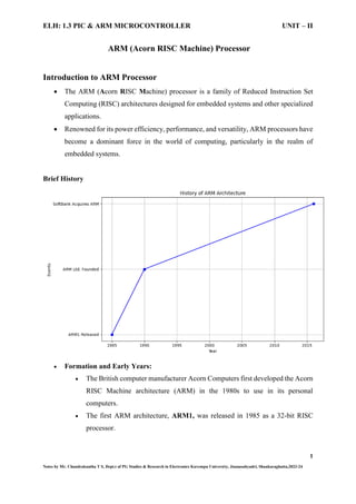
  • 1. ELH: 1.3 PIC & ARM MICROCONTROLLER UNIT – II 1 Notes by Mr. Chandrakantha T S, Dept.t of PG Studies & Research in Electronics Kuvempu University, Jnanasahyadri, Shankaraghatta,2023-24 ARM (Acorn RISC Machine) Processor Introduction to ARM Processor  The ARM (Acorn RISC Machine) processor is a family of Reduced Instruction Set Computing (RISC) architectures designed for embedded systems and other specialized applications.  Renowned for its power efficiency, performance, and versatility, ARM processors have become a dominant force in the world of computing, particularly in the realm of embedded systems. Brief History  Formation and Early Years:  The British computer manufacturer Acorn Computers first developed the Acorn RISC Machine architecture (ARM) in the 1980s to use in its personal computers.  The first ARM architecture, ARM1, was released in 1985 as a 32-bit RISC processor.
  • 2. ELH: 1.3 PIC & ARM MICROCONTROLLER UNIT – II 2 Notes by Mr. Chandrakantha T S, Dept.t of PG Studies & Research in Electronics Kuvempu University, Jnanasahyadri, Shankaraghatta,2023-24  Evolution and Partnerships:  In 1990, ARM Ltd. was founded as a joint venture between Acorn, Apple, and VLSI Technology.  The ARM architecture continued to evolve, with subsequent versions offering enhanced performance and features.  Widespread Adoption:  ARM gained significant traction in the 1990s and 2000s, becoming the architecture of choice for many mobile devices, including smartphones and tablets.  Business Model:  ARM operates on a licensing model, allowing other companies to use its architecture in their designs. This approach has contributed to the widespread adoption of ARM processors across various industries.  Acquisition by SoftBank:  In 2016, SoftBank Group acquired ARM Holdings, marking a significant development in the history of the company. ARM Core:  Definition:  The term "ARM core" refers to the central processing unit (CPU) design based on ARM architecture. ARM cores are the fundamental building blocks of ARM processors.  It's important to note that ARM, as a company, specializes in designing and licensing intellectual property (IP) rather than manufacturing silicon.
  • 3. ELH: 1.3 PIC & ARM MICROCONTROLLER UNIT – II 3 Notes by Mr. Chandrakantha T S, Dept.t of PG Studies & Research in Electronics Kuvempu University, Jnanasahyadri, Shankaraghatta,2023-24  ARM follows a licensing model where it designs CPU architectures and licenses them to semiconductor manufacturers. These manufacturers then integrate ARM cores into their own system-on-chip (SoC) designs. As a result, ARM does not manufacture silicon directly but rather collaborates with various semiconductor companies.  ARM is one of the most licensed and thus widespread processor cores in the world.  Core Families:  ARM cores are categorized into families based on their architectural features and capabilities. Common core families include ARM Cortex-A, Cortex-R, and Cortex-M. Classification of ARM Processor Families There are 3 types of ARM processors specifically designed for various purposes
  • 4. ELH: 1.3 PIC & ARM MICROCONTROLLER UNIT – II 4 Notes by Mr. Chandrakantha T S, Dept.t of PG Studies & Research in Electronics Kuvempu University, Jnanasahyadri, Shankaraghatta,2023-24 1. Cortex-A Series:  Usage: Primarily used in applications requiring high performance and running operating systems (OS), such as Smart TV, smartphones, tablets, and automotive infotainment systems.  Features: Multicore support, advanced pipeline architecture.  Architecture: ARMv7-A, ARMv8-A (64-bit)  Examples of Cortex-A Series: Cortex-A53, Cortex-A72, Cortex-A76. Qualcomm Snapdragon 865: Found in high-end smartphones, providing powerful processing capabilities. NVIDIA Tegra X1: Used in applications like gaming consoles and automotive displays, delivering high-performance graphics. 2. Cortex-R Series:  Usage: Employed in real-time applications demanding high reliability and predictability, such as automotive safety systems (Air Bag) and industrial control systems.  Features: Designed for real-time processing, often includes features for error detection and correction.  Architecture: ARMv7-R, ARMv8-R (64-bit)  Examples of Cortex-R Series: Cortex-R4, Cortex-R5. NXP S32R27: Applied in automotive applications like radar systems, providing real-time processing for collision detection. Altera Cyclone V: Utilized in industrial control systems, offering reliable real- time processing for automation. 3. Cortex-M Series:  Usage: Geared towards microcontroller applications with a focus on low power, real- time responsiveness, and cost-effectiveness. Widely used in IoT devices.  Features: Low-power design, efficient interrupt handling, simple architecture suitable for microcontroller applications.  Architecture: ARMv6-M, ARMv7-M, ARMv8-M (for security enhancements) (32-bit)
  • 5. ELH: 1.3 PIC & ARM MICROCONTROLLER UNIT – II 5 Notes by Mr. Chandrakantha T S, Dept.t of PG Studies & Research in Electronics Kuvempu University, Jnanasahyadri, Shankaraghatta,2023-24  Examples of Cortex-M Series: Cortex-M0, Cortex-M3(NXP LPC2148), Cortex-M4, Cortex-M7. STM32F4: Popular in various microcontroller applications, including IoT devices and consumer electronics. Nordic Semiconductor nRF52: Found in Bluetooth-enabled IoT devices, emphasizing low power consumption and real-time responsiveness. NXP LPC2148: This microcontroller is based on the ARM7TDMI-S core, providing a balance of performance and power efficiency. Widely used in various embedded systems, including industrial control, automotive applications, and consumer electronics. Nomenclature(Naming) of ARM The nomenclature or naming convention for ARM-based microcontrollers, like the LPC2148, typically follows a pattern that provides information about the device's features and specifications. [Prefix][Core Family]-[Series Number][Device Specific Identifier]  L: ARM7 M3 family (Low Power Consumption series)  P: Packaged in a certain way (e.g., QFP). Low-Profile Quad Flat Package (LQFP)  C: The "C" signifies the core type. Based on the ARM7TDMI-S core.  21: Part of a specific series, indicating a set of shared characteristics.  48: A device-specific identifier, providing details about this particular member within the series. ARM7TDMI-S  ARM- Advanced RISC Machine  T-Thumb2 (16 Bit Compressed Instruction Set)  D-Debug  M- Multiply(Hardware)  I-S-Interrupt – Standard (Standard Interrupt Handling Capabilities)
  • 6. ELH: 1.3 PIC & ARM MICROCONTROLLER UNIT – II 6 Notes by Mr. Chandrakantha T S, Dept.t of PG Studies & Research in Electronics Kuvempu University, Jnanasahyadri, Shankaraghatta,2023-24 Introduction to Embedded Systems  Embedded systems are specialized computing systems designed to perform dedicated functions within a larger system.  Unlike general-purpose computers, embedded systems are tailored for specific applications and are often part of everyday devices such as washing machines, cars, medical devices, and more.  They play a crucial role in controlling and monitoring various functions in real-time. An embedded system is a combination of hardware(Microcontroller) and software (Collection of program) designed to perform a dedicated function  "Embedded" refers to something firmly fixed or deeply integrated into a surrounding matrix. In the context of technology, it denotes the integration of specialized computing components, such as microcontrollers or processors, into a larger system or device to perform specific functions.  "Systems" refer to organized and interconnected sets of elements or components that work together to achieve a common purpose or function. In the context of embedded systems, this encompasses the integration of hardware and software components designed to perform specific tasks. Block diagram of Embedded System In an embedded system, various components work together to achieve a specific function. 1. Sensor:  Function: Sensors are devices that convert physical or environmental parameters (such as temperature, pressure, or light) into electrical signals.
  • 7. ELH: 1.3 PIC & ARM MICROCONTROLLER UNIT – II 7 Notes by Mr. Chandrakantha T S, Dept.t of PG Studies & Research in Electronics Kuvempu University, Jnanasahyadri, Shankaraghatta,2023-24  Example in Embedded System: A temperature sensor in a climate control system measures the ambient temperature. 2. A-D Converter (Analog-to-Digital Converter):  Function: The A-D converter converts analog signals from sensors into digital signals that can be processed by the microcontroller or processor.  Example in Embedded System: The analog signal from a temperature sensor is converted into a digital format for processing. 3. Processor & ASICs (Application-Specific Integrated Circuits):  Function: The processor and ASICs handle the processing and control functions of the embedded system. They execute the software and algorithms necessary for the system's operation.  Example in Embedded System: A microcontroller processes the digital temperature data and decides whether to activate the air conditioning system. 4. D-A Converter (Digital-to-Analog Converter):  Function: The D-A converter converts digital signals from the processor back into analog signals. This is necessary for interfacing with analog components like actuators.  Example in Embedded System: The digital output from the microcontroller, determining the desired temperature setting, is converted into an analog signal to control the air conditioning unit. 5. Actuator:  Function: Actuators are devices that perform physical actions based on electronic signals. They translate electrical signals into mechanical or physical actions.  Example in Embedded System: An actuator in a climate control system adjusts the vents or activates the heating or cooling elements based on the processed temperature data.
  • 8. ELH: 1.3 PIC & ARM MICROCONTROLLER UNIT – II 8 Notes by Mr. Chandrakantha T S, Dept.t of PG Studies & Research in Electronics Kuvempu University, Jnanasahyadri, Shankaraghatta,2023-24 Climate Control System Key Characteristics of Embedded Systems: 1. Dedicated Functionality:  Embedded systems are designed for specific, predefined functions or tasks. They are tailored to perform a dedicated role within a larger system. 2. Real-Time Operation:  Many embedded systems operate in real-time, meaning they must respond to inputs or stimuli within a defined time frame. This is crucial for applications where timely and predictable responses are essential. 3. Hardware-Software Integration:  These systems consist of both hardware and software components intricately integrated to achieve the desired functionality. Microcontrollers or specialized processors are often employed as the central processing unit. 4. Single-Purpose Devices:  Unlike general-purpose computers, embedded systems are typically single- purpose devices. They are not intended for running a variety of applications but rather focus on specific tasks. 5. Resource Constraints:  Embedded systems often have limitations in terms of processing power, memory, and storage. These resource constraints are balanced to meet the requirements of the targeted application efficiently. 6. Compact and Power-Efficient:
  • 9. ELH: 1.3 PIC & ARM MICROCONTROLLER UNIT – II 9 Notes by Mr. Chandrakantha T S, Dept.t of PG Studies & Research in Electronics Kuvempu University, Jnanasahyadri, Shankaraghatta,2023-24  Embedded systems are designed to be compact and power-efficient, making them suitable for integration into various devices, ranging from household appliances to industrial machinery. ARM Cortex-M3: Addressing the 32-Bit Embedded Processor Market The ARM (Cortex-M3) addresses the requirements for the 32-bit embedded processor market in the following ways: 1. Greater performance efficiency: allowing more work to be done without increasing the frequency or power requirements. 2. Low power consumption: enabling longer battery life, especially critical in portable products including wireless networking applications. 3. Enhanced determinism: guaranteeing that critical tasks and interrupts are serviced as quickly as possible and in a known number of cycles. 4. Improved code density: ensuring that code fits in even the smallest memory footprints. 5. Ease of use: providing easier programmability and debugging for the growing number of 8-bit and 16-bit users migrating to 32 bits. 6. Lower cost solutions: reducing 32-bit-based system costs close to those of legacy 8- bit and 16-bit devices and enabling low-end, 32-bit microcontrollers to be priced at less than US$1 for the first time. 7. Wide choice of development tools: from low-cost or free compilers to full-featured development suites from many development tool vendors
  • 10. ELH: 1.3 PIC & ARM MICROCONTROLLER UNIT – II 10 Notes by Mr. Chandrakantha T S, Dept.t of PG Studies & Research in Electronics Kuvempu University, Jnanasahyadri, Shankaraghatta,2023-24 Applications of ARM-based Embedded Systems: 1. Consumer Electronics:  Smartphones, tablets, smart TVs, and other consumer devices often use ARM- based processors for their compact design and power efficiency. 2. Automotive Systems:  ARM processors are employed in various automotive applications, including engine control units, infotainment systems, and Advanced Driver-Assistance Systems (ADAS). 3. Industrial Automation:  Embedded systems with ARM processors play a crucial role in industrial automation for tasks such as process control, monitoring, and data acquisition. 4. Healthcare Devices:  Medical devices, wearable health trackers, and diagnostic equipment leverage ARM-based embedded systems for their computational efficiency and low power consumption. 5. Internet of Things (IoT):  ARM processors are extensively used in IoT devices for their ability to connect, process data, and operate with minimal power consumption. ARM-based embedded systems offer a powerful and flexible solution for a wide range of applications, contributing to the advancement of technology in various industries.
  • 11. ELH: 1.3 PIC & ARM MICROCONTROLLER UNIT – II 11 Notes by Mr. Chandrakantha T S, Dept.t of PG Studies & Research in Electronics Kuvempu University, Jnanasahyadri, Shankaraghatta,2023-24 ARM Processor Fundamentals General Salient Features of ARM Cortex-M3 Processor Feature Description 1. Architecture RISC (Reduced Instruction Set Computer) architecture developed by Advanced RISC Machines (ARM) and Harvard memory architecture 2. Data Path 32-bit microprocessor(CPU) with a 32-bit data path (ALU), 32-bit registers, and 32-bit memory interfaces. 3. Bus Technology AMBA (Advanced Microcontroller Bus Architecture) - follows the Harvard bus architecture. 4. Instruction Set Architecture Load/Store Architecture. 5. Pipeline 3-Stage Pipeline(FDE) 6. Registers ARM has 37 registers each of 32-bit length  31[R0-R15] General Purpose Registers  6 [CPSR,SP,LR]Special Purpose Register 7. Thumb-2 Instruction Technology Thumb-2 instruction set technology allows the use of both 32-bit and 16-bit instructions. 8. Operation Modes Two operation modes: Thread mode and Handler mode. 9. Access Levels Two access levels: Privileged Level and User Level. 10. Operating Frequency Up to 100 MHz 11. Interrupts and Exceptions Built-in Nested Vectored Interrupt Controller (NVIC) supporting non-maskable interrupts and 1 to 240 physical interrupts with 8 to 256 priority levels. 12. Memory Protection Unit (MPU) Manages the CPU's access to memory, preventing tasks from accidentally corrupting memory or resources used by other tasks. 13. Tightly Coupled Memory (TCM) ARM processors have tightly coupled memory for fast response times and low latency, useful in cases where cache memory behavior is unpredictable. 14. Debug and Trace  Debug technology provides useful trace information via a standard JTAG connector without the need for costly hardware
  • 12. ELH: 1.3 PIC & ARM MICROCONTROLLER UNIT – II 12 Notes by Mr. Chandrakantha T S, Dept.t of PG Studies & Research in Electronics Kuvempu University, Jnanasahyadri, Shankaraghatta,2023-24  JTAG (Joint Test Action Group):an industry standard for verifying designs and testing printed circuit boards after manufacture. Pinout of NXP LPC2148
  • 13. ELH: 1.3 PIC & ARM MICROCONTROLLER UNIT – II 13 Notes by Mr. Chandrakantha T S, Dept.t of PG Studies & Research in Electronics Kuvempu University, Jnanasahyadri, Shankaraghatta,2023-24 Salient Features of NXP LPC2141/42/44/46/48 (ARM Cortex-M3) Feature Description Processor 16-bit/32-bit ARM7TDMI-S Package LQFP Memory On-chip static RAM: 8 kB to 40 kB; On-chip flash memory: 32 kB to 512 kB Speed 60 MHz operation with a 128-bit wide interface/accelerator Programming In-System Programming/In-Application Programming (ISP/IAP) via on-chip bootloader software USB Support USB 2.0 Full-speed compliant device controller with 2 kB of endpoint RAM Debugging EmbeddedICE RT and Embedded Trace interfaces for real-time debugging Analog Features One or two 10-bit ADCs providing 6/14 analog inputs; Single 10-bit DAC for variable analog output Timers and PWM Two 32-bit timers/external event counters, PWM unit with six outputs, and watchdog Communication Interfaces Multiple serial interfaces, including two UARTs (16C550), two Fast I2C-bus, SPI, and SSP(Synchronous Serial Port) Interrupts Nested Vectored Interrupt Controller (NVIC) with configurable priorities and vector addresses GPIO Up to 45 fast general-purpose I/O pins, 21 external interrupt pins Clocking Programmable on-chip PLL with a maximum CPU clock of 60 MHz, integrated oscillator from 1 MHz to 25 MHz Power Management Power saving modes (Idle and Power-down), individual enable/disable of peripheral functions, and peripheral clock scaling Supply Voltage 3.0 V to 3.6 V (3.3 V ± 10%) with 5 V tolerant I/O pads Wake-up Mechanism Processor wake-up from Power-down mode via external interrupt or Brown-out Detection (BOD)
  • 14. ELH: 1.3 PIC & ARM MICROCONTROLLER UNIT – II 14 Notes by Mr. Chandrakantha T S, Dept.t of PG Studies & Research in Electronics Kuvempu University, Jnanasahyadri, Shankaraghatta,2023-24 Block Diagram of NXP LPC2141/42/44/46/48
  • 15. ELH: 1.3 PIC & ARM MICROCONTROLLER UNIT – II 15 Notes by Mr. Chandrakantha T S, Dept.t of PG Studies & Research in Electronics Kuvempu University, Jnanasahyadri, Shankaraghatta,2023-24 Architecture of ARM Cortex M3  The ARM Cortex-M3 is a 32-bit RISC (Reduced Instruction Set Computing) processor designed by ARM Holdings.  It is part of the Cortex-M family, which specifically targets microcontroller and embedded system applications.  The Cortex-M3 processor is known for its balance between performance, power efficiency, and ease of use, making it a popular choice in a wide range of embedded systems. Architecture  The Cortex-M3 (ARM7TDMI-S) follows a load-store architecture, where data processing is performed only in registers, Direct manipulation of memory is not allowed.  It employs a 32-bit RISC instruction set, which means instructions are typically simple and execute in a single clock cycle, contributing to efficient and predictable performance.
  • 16. ELH: 1.3 PIC & ARM MICROCONTROLLER UNIT – II 16 Notes by Mr. Chandrakantha T S, Dept.t of PG Studies & Research in Electronics Kuvempu University, Jnanasahyadri, Shankaraghatta,2023-24  The processor features a Harvard architecture with separate buses for instruction and data. This allows simultaneous instruction fetches and data accesses, improving overall system performance.  The Cortex-M3 utilizes a 3-stage pipeline, enabling the execution of multiple instructions concurrently. This contributes to higher throughput and better performance.
  • 17. ELH: 1.3 PIC & ARM MICROCONTROLLER UNIT – II 17 Notes by Mr. Chandrakantha T S, Dept.t of PG Studies & Research in Electronics Kuvempu University, Jnanasahyadri, Shankaraghatta,2023-24  The Advanced Microcontroller Bus Architecture (AMBA) bus connects the Cortex- M3 processor to external components like memory, peripherals, and debug interfaces.  The ARM7TDMI-S processor, while the primary instruction set is 32-bit, the Cortex- M3 also supports the Thumb instruction set. Thumb instructions are 16-bit, providing increased code density without sacrificing performance significantly.  Both little-endian and big-endian memory systems are supported. This flexibility allows the Cortex-M3 to adapt to different memory organization requirements in various applications. Processor Core System Components Interrupts and NVIC (Nested Vectored Interrupt Controller):  Handles interrupts and manages their priorities.  The NVIC efficiently supports nested interrupts and allows the processor to respond to multiple interrupt sources. Instruction Fetch Unit:  Responsible for fetching instructions from memory.  Coordinates with the decoder to interpret and execute instructions.
  • 18. ELH: 1.3 PIC & ARM MICROCONTROLLER UNIT – II 18 Notes by Mr. Chandrakantha T S, Dept.t of PG Studies & Research in Electronics Kuvempu University, Jnanasahyadri, Shankaraghatta,2023-24 Decoder:  Decodes fetched instructions into control signals for various components.  Directs the flow of execution based on the decoded instructions. ALU (Arithmetic Logic Unit):  Performs arithmetic and logic operations on data.  Executes the actual computation specified by the decoded instructions. Register Bank:  Holds 32 bit general-purpose registers used for data manipulation during program execution.  Provides a fast and direct way for the processor to operate on data. Memory Interface and Bus Interconnect(AMBA):  Manages the flow of data between different components within the processor core system.  Coordinates data transfer between the processor core, memory, and peripherals (Instruction Bus, Data Bus). Memory Protection Unit (MPU):  Optional component that enhances security and control over memory access.  Allows setting regions of memory as read-only or no access, improving the robustness of the system. Debugger System:  Includes various debugging components, such as breakpoints and watchpoints.  Aids developers in identifying and resolving issues during program development. Trace Interface:  Part of the debugger system.  Provides the ability to trace and monitor the execution flow of the program for debugging purposes.
  • 19. ELH: 1.3 PIC & ARM MICROCONTROLLER UNIT – II 19 Notes by Mr. Chandrakantha T S, Dept.t of PG Studies & Research in Electronics Kuvempu University, Jnanasahyadri, Shankaraghatta,2023-24 Code Memory:  Holds program instructions for execution.  Accessed through the code memory bus. Memory System and Peripherals:  Interacts with the memory system and various peripherals (ADC/DAC, Timer/Counter).  Coordinated through the memory system bus. Private Peripherals:  Connects to specific on-chip peripherals (Watchdog Timer (WDT), Real-Time Clock (RTC))  Efficient communication is facilitated through the private peripheral bus. ARM Core(ALU) Dataflow Model The ARM Core(ALU) Dataflow Model describes the flow of data and operations within the Arithmetic Logic Unit (ALU) of an ARM processor.
  • 20. ELH: 1.3 PIC & ARM MICROCONTROLLER UNIT – II 20 Notes by Mr. Chandrakantha T S, Dept.t of PG Studies & Research in Electronics Kuvempu University, Jnanasahyadri, Shankaraghatta,2023-24  A programmer can think of an ARM core as functional units connected by data buses, as shown in Figure, where, the arrows represent the flow of data, the lines represent the buses, and the boxes represent either an operation unit or a storage area.  The figure shows not only the flow of data but also the abstract components that make up an ARM core.  Data enters the processor core through the Data bus. The data may be an instruction to execute or a data item. Instruction Decoder  The instruction decoder interprets the machine code instructions fetched from memory.  It identifies the operation to be performed, the operands involved, and the destination for the result.  Example: Given the instruction ADD R1, R2, R3, the instruction decoder recognizes it as an addition operation. It identifies R2 and R3 as source operands and R1 as the destination register. Register File:  The register file is a set(bank) of 32 bit registers that stores operands for ALU operations and holds the results.  The operands are typically sourced from these registers, and the results are written back to them.  Most operations involving data processing occur within these registers.  Example: If R2 contains the value 5 and R3 contains 7, the register file provides these operands to the ALU for the addition operation. Sign Extender:  Sign extend hardware ensures proper conversion of signed 8-bit and 16-bit numbers to 32-bit values as they are read from memory.  The extended values are used in subsequent calculations.  Example: Sign Extension of 8-bit Signed Number to 32-bit  Suppose we have an 8-bit signed number stored in memory: Data: 11011011
  • 21. ELH: 1.3 PIC & ARM MICROCONTROLLER UNIT – II 21 Notes by Mr. Chandrakantha T S, Dept.t of PG Studies & Research in Electronics Kuvempu University, Jnanasahyadri, Shankaraghatta,2023-24  In this example, the most significant bit (MSB) is 1, indicating a negative number in two's complement representation. To sign-extend this 8-bit value to a 32-bit value, we replicate the sign bit (1) to fill the additional 24 bits.  Sign-Extended 32-bit Value: 11111111 11111111 11111111 11011011 ALU (Arithmetic Logic Unit):  The ALU performs arithmetic and logic operations based on decoded instructions.  Arithmetic operations include addition, subtraction, and multiplication, while logic operations involve bitwise operations like AND, OR, and XOR.  Source operands are fetched from the register file (Rn and Rm) using internal buses A and B.  Resulting data is written directly to the register file (Rd) for data processing instructions.  For load and store instructions, the ALU generates addresses for data transfer.  Example: The ALU adds the values from R2 and R3 together, resulting in 12. The result is then stored in R1. MAC (Multiply-Accumulate Unit):  The Multiply-Accumulate Unit is a specialized component that performs a combined multiply and accumulate operation.  It is often used in signal processing applications, such as digital signal processing (DSP).  Example: In a DSP application, if there's an instruction like MAC R1, R2, R3, the MAC unit would multiply the values in R2 and R3, then add the result to the value already in R1. Barrel Shifter:  The barrel shifter preprocesses register values (Rm) before entering the ALU.
  • 22. ELH: 1.3 PIC & ARM MICROCONTROLLER UNIT – II 22 Notes by Mr. Chandrakantha T S, Dept.t of PG Studies & Research in Electronics Kuvempu University, Jnanasahyadri, Shankaraghatta,2023-24  The barrel shifter is responsible for shifting and rotate the bits of an operand left or right.  It supports both logical and arithmetic shifts and is used in various operations, including multiplication and division.  Example: If there's an instruction LSL R1, R2, #2, the barrel shifter would shift the bits in R2 two positions to the left, effectively multiplying the value by 4, and store the result in R1. MOV R2, #5 ; Load value 5 into R2 MOV R1, #0 ; Initialize R1 to 0 LSL R1, R2, #2 ; Logical shift left R2 by 2 positions and store result in R1 Before the instruction R2 = 5 (binary: 0101) After the instruction R2 = 010100 So, after executing the instruction R1 = 20 (decimal) or 14 (hexadecimal) Address Register and Incrementer:  For load and store instructions, the incrementer updates the address register.  Sequential memory locations are accessed by updating the address before each read or write operation.
  • 23. ELH: 1.3 PIC & ARM MICROCONTROLLER UNIT – II 23 Notes by Mr. Chandrakantha T S, Dept.t of PG Studies & Research in Electronics Kuvempu University, Jnanasahyadri, Shankaraghatta,2023-24  Example: In a loop where you're accessing elements in an array, the address register holds the base address of the array, and the incrementer calculates the next address for the next iteration. Result Bus:  The Result bus is used to write the result of data processing operations back to the register file. Execution Flow:  The processor continues executing instructions until an exception or interrupt alters the normal flow of execution. Advanced Microcontroller Bus Architecture(AMBA) of ARM Cortex M3  The Advanced Microcontroller Bus Architecture (AMBA) for the ARM Cortex-M3 processor is designed to provide a standardized and efficient communication infrastructure within microcontroller and System-on-Chip (SoC) designs.  System-on-Chip (SoC) integrates essential computer elements on a single chip, such as CPU, RAM, UART, and peripherals.  The AMBA addresses the challenge of efficiently connecting and managing these subsystems in SoCs PIO: Programmable Input/Output
  • 24. ELH: 1.3 PIC & ARM MICROCONTROLLER UNIT – II 24 Notes by Mr. Chandrakantha T S, Dept.t of PG Studies & Research in Electronics Kuvempu University, Jnanasahyadri, Shankaraghatta,2023-24 The AMBA specification defines three main buses: 1.Advanced High-Performance Bus (AHB):  The AHB serves as the backbone of the system, designed for high-performance and high-frequency components.  Connects high-performance components such as processors, on-chip memories, and memory interfaces.  Operates with a single clock edge for improved performance.  Supports wider data buses, such as 64/128 bits, for enhanced data transfer rates.  Example: Efficiently handing over control of the bus from the processor to a DMA (Direct Memory Access) controller within a single clock cycle. 2.Adanced System Bus (ASB):  The ASB is an alternative to the AHB, providing high performance for 16- and 32-bit systems.  Connects components that do not require the advanced features of the AHB.  Shares many signals with the AHB, simplifying the transition between the two buses.  Offers high performance for systems with lower complexity. 3. Advanced Peripheral Bus (APB):  The APB is a simplified interface designed for low-bandwidth peripherals that do not require the high performance of the AHB or ASB.  Connects low-frequency peripherals like UART, GPIO, and timers.  All signal transitions are synchronized to the rising edge of the clock. An example of an ARM-based embedded device, a microcontroller Rising and Falling Edge of Clock
  • 25. ELH: 1.3 PIC & ARM MICROCONTROLLER UNIT – II 25 Notes by Mr. Chandrakantha T S, Dept.t of PG Studies & Research in Electronics Kuvempu University, Jnanasahyadri, Shankaraghatta,2023-24  Consists of a single bus master called the APB bridge, which acts as a slave on the AHB/ASB.  The APB bridge serves as the interface between high-performance buses and low- frequency peripherals.  Peripheral devices on the APB are the slaves. AHB to APB Bridge  It manages the conversion of signals and timing considerations between the faster AHB and the slower APB. ASB to APB Bridge  Like the AHB to APB Bridge, the ASB to APB Bridge enables communication between components on the high-performance ASB and peripherals on the low-frequency APB Programmer's Model of ARM Cortex M3  The programmer's model of the ARM Cortex-M3 includes registers and memory organization that provide an interface for software developers to interact with the processor.  It includes information about the CPU registers, instruction set, and the overall programming environment. I)Registers Organization of ARM Cortex M3  The Cortex-M3 processor has registers total of 37 register each of 32-bits long are classified into 2 groups i) 28 General-Purpose Register(GPR) iii) 9 Special-Purpose Register(SPR)  ARM based systems are designed to be operated in 7 modes. These modes have their own specifications in operation and accessibility to the register sets.  Up to 18 active registers are available: 16 data registers and 2 processor status registers. The data registers are labeled r0 through r15 by the programmer.
  • 26. ELH: 1.3 PIC & ARM MICROCONTROLLER UNIT – II 26 Notes by Mr. Chandrakantha T S, Dept.t of PG Studies & Research in Electronics Kuvempu University, Jnanasahyadri, Shankaraghatta,2023-24  The ARM processor contains three registers: r13, r14, and r15, each of which is allocated to a specific duty or unique function. To distinguish them from the other registers, they are typically given separate labels. The Shaded registers indicate which special-purpose registers have been allocated.  These registers play a crucial role in data processing, control flow, and system status management. i)28 General-Purpose Register (GPR) [R0-R12, (R0-R7 Low GPR) (R8-R12 High GPR, 15 BGPR] General-purpose registers hold either data or an address. They are identified with the letter r prefixed to the register number. For example, register 4 is given the label r4.
  • 27. ELH: 1.3 PIC & ARM MICROCONTROLLER UNIT – II 27 Notes by Mr. Chandrakantha T S, Dept.t of PG Studies & Research in Electronics Kuvempu University, Jnanasahyadri, Shankaraghatta,2023-24 a) Low GPR (R0-R7):  The R0 through R7 general purpose registers are also called low registers. They can be accessed by all 16-bit Thumb instructions and all 32-bit Thumb-2 instructions.  They are all 32 bits; the reset value is unpredictable. b) High GPR (R8-R12):  The R8 through R12 registers are also called high registers. They are accessible by all Thumb-2 instructions but not by all 16-bit Thumb instructions.  These registers are all 32 bits; the reset value is unpredictable. c)Banked General-Purpose Registers (BGPR):  There are 15 banked general-purpose registers that cater to specific processor modes.  These registers provide context-specific storage, allowing for efficient mode transitions and context switching. Example: 1) FIQ (Fast Interrupt Request) Mode:  In FIQ mode, R8_fiq, R9_fiq, R10_fiq, R11_fiq, and R12_fiq are the banked registers. 2) IRQ (Interrupt Request) Mode:  In IRQ mode, R8_irq, R9_irq, R10_irq, R11_irq, and R12_irq are the banked registers. 3)Supervisor Mode (SVC):  In Supervisor mode, R8_svc, R9_svc, R10_svc, R11_svc, and R12_svc are the banked registers. 4)Abort Mode (ABT):  In Abort mode, R8_abt, R9_abt, R10_abt, R11_abt, and R12_abt are the banked registers. 5)Undefined Mode (UND):  In Undefined mode, R8_und, R9_und, R10_und, R11_und, and R12_und are the banked registers.
  • 28. ELH: 1.3 PIC & ARM MICROCONTROLLER UNIT – II 28 Notes by Mr. Chandrakantha T S, Dept.t of PG Studies & Research in Electronics Kuvempu University, Jnanasahyadri, Shankaraghatta,2023-24 Note: 1)Contextual Use of r13 and r14:  r13 (Stack Pointer) and r14 (Link Register) can be used as general-purpose registers in specific contexts.  Advantage: These registers are banked during a processor mode change, facilitating efficient mode transitions and context switching.  Caution: Using r13 as a general register in the presence of an operating system is risky, as operating systems typically assume r13 always points to a valid stack frame. 2)Orthogonality of r0 to r13 in ARM State:  In ARM state (32 bit), registers r0 to r13 are orthogonal, meaning any instruction applicable to r0 can be used with any other register in this range.  Special Treatment for r14 and r15: Instructions treating r14 (Link Register) and r15 (Program Counter) exist and are handled differently. 3)Register Visibility Depending on Processor Mode:  The register file contains all registers available to a programmer.  Register visibility depends on the current mode of the processor.  Different processor modes may have specific sets of visible registers. ii) 9 Special-Purpose Register(SPR) [ SP, LR, PC, CPSR, 5 SPSR] The Special-Purpose Registers (SPR) in ARM Cortex-M3 play crucial roles in controlling program execution, managing exceptions, and preserving critical information. 1) Stack Pointer (SP):  Register r13 is traditionally used as the stack pointer (sp) and holds the address of the top of the stack, which is essential for managing the program stack.  The primary operations associated with a stack are push and pop. Example LDR R0, =0x4000000C ; Load the base address of the stack into R0 MOV SP, R0 ; Set the Stack Pointer to the base address
  • 29. ELH: 1.3 PIC & ARM MICROCONTROLLER UNIT – II 29 Notes by Mr. Chandrakantha T S, Dept.t of PG Studies & Research in Electronics Kuvempu University, Jnanasahyadri, Shankaraghatta,2023-24 PUSH {R0} [SP40000008] PUSH {R0} [SP40000004] POP {R0} [ SP40000008] Address Register (AR): This register points at the collection of data and is used during the execute phase to read an operand. ADD R3, R2,R1 2)Link Register (r_ 14 LR): Register r14 is called the link register (lr) stores the return address for subroutines and is automatically loaded with the address following a branch or jump instruction. Example BL MySubroutine ; Branch with Link to MySubroutine ; The return address is stored in LR 3)Program Counter (r_15 PC): Register r15 is the program counter (pc) and contains the address of the next instruction to be fetched by the processor, serving as the instruction pointer.
  • 30. ELH: 1.3 PIC & ARM MICROCONTROLLER UNIT – II 30 Notes by Mr. Chandrakantha T S, Dept.t of PG Studies & Research in Electronics Kuvempu University, Jnanasahyadri, Shankaraghatta,2023-24 Example: PC=0x00000000 MOV R0, #10 ; Load the value 10 into R0 [PC=0x000000004] ADD R1, R0, #5 ; Add 5 to R0 and store the result in R1[PC=0x00000008] Program Status Registers (PSRs) cpsr (Current Program Status Register) and spsr (Saved Program Status Register) are the two program status registers. i) Current Processor Status Register (CPSR):  The CPSR is a 32-bit register residing in the ARM Cortex-M3 register file.  It is dedicated to monitoring and controlling internal operations during instruction execution, contains flags for conditional codes, processor status information, and the current processor mode.
  • 31. ELH: 1.3 PIC & ARM MICROCONTROLLER UNIT – II 31 Notes by Mr. Chandrakantha T S, Dept.t of PG Studies & Research in Electronics Kuvempu University, Jnanasahyadri, Shankaraghatta,2023-24 a) Condition Flags Bits (N, Z, C, V):  The N, Z, C, and V are the 4 bits of condition flags from bit 28 to 30 in CPSR. 1. N (Negative) Flag (bit 31): Set to 1 if the result of an operation is negative, otherwise set to 0. 2. Z (Zero) Flag (bit 30): Set to 1 if the result of an operation is zero, otherwise reset to 0. 3. C (Carry) Flag (bit 29): Set to 1 if there is a carry-out or borrow into the most significant bit, otherwise reset to 0. 4. V (Overflow) Flag (bit 28): Set to 1 if there is signed overflow, otherwise reset to 0.  These flags provide information about the result of arithmetic and logical operations, aiding in conditional branching and decision-making within a program.  Condition flags are updated by ALU when performs the Arithmetic, Logical, and Shifting operations that specify the S instruction suffix. Eg: ADDS, SUBS Examples: 1) LDR R1, =0x12345678 LDR R2, =0xF7654321 ADDS R3, R1, R2
  • 32. ELH: 1.3 PIC & ARM MICROCONTROLLER UNIT – II 32 Notes by Mr. Chandrakantha T S, Dept.t of PG Studies & Research in Electronics Kuvempu University, Jnanasahyadri, Shankaraghatta,2023-24 00010010001101000101011001111000 + 11110111011001010100001100100001 ------------------------------------------------------ 0100001001100110011001100110011001 Affected Flags NZCV=0010 2) LDR R1, =0x87654321 LDR R2, =0xAFFFFFFF SUBS R5, R1, R2 R1 (smaller) = 1000 0111 0110 0101 0100 0011 0010 0001 R2 (larger) = 1010 1111 1111 1111 1111 1111 1111 1111 ------------------------------------------------------------------------- R5 (result) = -0101000100110101011110011011110 Affected Flags NZCV=1000 b) Control Flag Bits The 8 bits from 0 to 7 of CPSR are known collectively as the control bits, they are the 1. Interrupt Disable Bits (I, F):  I (Interrupt Disable): When set (I=1), interrupts are globally disabled. This is crucial for critical sections where interrupt handling should be postponed.  F (Fast Interrupt Disable): When set (F=1), disables fast interrupts. Similar to I bit but specifically for fast interrupts. 2. T Bit (Thumb State):  T (Thumb State): When set (T=1), the processor is in Thumb state, executing 16-bit instructions.
  • 33. ELH: 1.3 PIC & ARM MICROCONTROLLER UNIT – II 33 Notes by Mr. Chandrakantha T S, Dept.t of PG Studies & Research in Electronics Kuvempu University, Jnanasahyadri, Shankaraghatta,2023-24  When clear (T=0), the processor is in ARM state, executing 32-bit instructions. Feature ARM (CPSR T = 0) Thumb (CPSR T = 1) Instruction Size 32-bit 16-bit Core Instructions 58 30 Conditional Execution Most instructions Only branch instructions Data Processing Instructions Access to barrel shifter and ALU Separate barrel shifter and ALU instructions Program Status Register (CPSR) Read-write in privileged mode No direct access Register Usage 13[R0-R12] general-purpose registers 8 [R0-R7]general-purpose registers 3. Mode Bits (M4:0)  The 5 bits M4, M3, M2, M1, and M0 bits (M [4:0]) of CPSR determine the processor's operating mode.  The combination of these bits defines the specific processor mode. M4 M3 M2 M1 M0 Processor Mode 0 0 0 0 0 User Mode(USR) 1 0 0 0 0 FIQ (Fast Interrupt Request) Mode 0 1 0 0 0 IRQ (Interrupt Request) Mode 0 0 1 0 0 Supervisor Mode (SVC) 0 0 0 1 0 Abort Mode (ABT) 0 0 0 0 1 Undefined Mode (UND) 1 1 1 1 1 System Mode(SYS)  Note: Not all combinations of the mode bits define a valid processor mode, so take care to use only the bit combinations shown ii) Saved Processor Status Registers (SPSR): Purpose of SPSR  There are five SPSR registers, each associated with a specific processor mode.  The SPSR is used to store the copy of the Current Program Status Register (CPSR) when an exception occurs.  It preserves the CPSR value before the processor switches to a different mode to handle an exception.
  • 34. ELH: 1.3 PIC & ARM MICROCONTROLLER UNIT – II 34 Notes by Mr. Chandrakantha T S, Dept.t of PG Studies & Research in Electronics Kuvempu University, Jnanasahyadri, Shankaraghatta,2023-24 Exception Handling  When an exception (such as an interrupt) occurs, the processor switches to a specific exception mode (e.g., FIQ mode).  Before this switch, the current CPSR value (representing the state of the processor) is stored in the corresponding SPSR for that exception mode. Access by Exception Handling Modes  Each exception handling mode has its own dedicated SPSR. For example, there are separate SPSR registers for IRQ, FIQ, Supervisor, Abort, and Undefined modes.  User mode and System mode do not have SPSRs since they are not exception handling modes. Banked Registers  When the processor mode changes due to an exception, banked registers associated with the new mode replace the existing registers.  For instance, in IRQ mode, r13_irq and r14_irq replace the regular r13 and r14 registers. The user mode registers (r13_usr and r14_usr) remain unaffected. MSR and MRS Instructions:  The Move to Special Register (MSR) and Move from Special Register (MRS) instructions are used to transfer data between general-purpose registers and special registers, including the CPSR and SPSRs. Example:
  • 35. ELH: 1.3 PIC & ARM MICROCONTROLLER UNIT – II 35 Notes by Mr. Chandrakantha T S, Dept.t of PG Studies & Research in Electronics Kuvempu University, Jnanasahyadri, Shankaraghatta,2023-24 ARM Cortex M3 Processor Modes and Access Levels  In the early days of computing, processors operated in a simple binary state – either executing instructions or handling interrupts.  However, with the evolution of technology, modern processors, such as those based on the ARM architecture, have become much more sophisticated and versatile. Processor modes  Processor modes, in the context of ARM processors, refer to the distinct operating environments that the processor can create for itself. These modes control how the processor interacts with system memory and manages tasks.  Unlike the early binary distinction between normal execution and interrupt handling, ARM processors support multiple modes that provide to different scenarios. Classification of ARM Cortex M3 Processor Modes and Access Levels  The ARM Cortex-M3 7 processor modes and 2 access levels are categorized based on the operating modes and privilege levels, providing a flexible environment for executing code and handling exceptions in achieving efficient and secure operation.
  • 36. ELH: 1.3 PIC & ARM MICROCONTROLLER UNIT – II 36 Notes by Mr. Chandrakantha T S, Dept.t of PG Studies & Research in Electronics Kuvempu University, Jnanasahyadri, Shankaraghatta,2023-24 I) Operating Modes  The ARM Cortex-M3 processor operates in two main modes: Thread Mode and Handler Mode.  These modes define whether the processor is executing regular program code or handling an exception, such as an interrupt.  Thread Mode and Handler Mode is controlled by the special register called the "CONTROL" register. CONTROL Register Bits: The "CONTROL" register is a 32-bit register with specific bits controlling various aspects of the processor modes:  CONTROL [1]:  Bit 1 is used to switch between the Thread and Handler modes.
  • 37. ELH: 1.3 PIC & ARM MICROCONTROLLER UNIT – II 37 Notes by Mr. Chandrakantha T S, Dept.t of PG Studies & Research in Electronics Kuvempu University, Jnanasahyadri, Shankaraghatta,2023-24  If CONTROL [1] =0is set to 0, the processor is in Thread Mode.  If CONTROL [1]=1 is set to 1, the processor is in Handler Mode.  CONTROL [0]:  Bit 0 is used to control the privilege level of the processor in Thread Mode.  If CONTROL[0] is set to 0, the processor operates in privileged mode.  If CONTROL[0] is set to 1, the processor operates in unprivileged mode. Transitions Between Privileged and Unprivileged Access Levels  Once program execution starts i.e. after reset, the processor starts execution in thread mode with privileged access level  Modifying CONTROL register's 0th bit to 1 forces the processor into unprivileged mode.  Once the processor is in unprivileged mode, it's not possible to access the CONTROL register and hence mode can not be changed.  The only way to revert to privileged mode from unprivileged mode is with the help of an exception.  Once an exception is generated, the appropriate exception handler will get executed in Handler mode. Since the Handler mode has a privileged access level, the user can update CONTOL register's 0th bit to 1, making the access level again privileged, after the exception handler exit.
  • 38. ELH: 1.3 PIC & ARM MICROCONTROLLER UNIT – II 38 Notes by Mr. Chandrakantha T S, Dept.t of PG Studies & Research in Electronics Kuvempu University, Jnanasahyadri, Shankaraghatta,2023-24 i) Thread Mode/ User mode [Privileged/Unprivileged access]  This is the primary operating mode for the Cortex-M3 processor.  In Thread mode, the processor executes application code and handles interrupts and exceptions.  Example: Running a user application, like a firmware program that reads sensor data and updates a display. ii)Handler Mode (Exceptions/ Interrupt)  Handler Mode is entered when the processor responds to an exception, such as an interrupt or a system exception.  Includes modes like Abort, Fast Interrupt Request (FIQ), Interrupt Request (IRQ), Supervisor (SVC), Undefined (UND), System (SYS), and User.
  • 39. ELH: 1.3 PIC & ARM MICROCONTROLLER UNIT – II 39 Notes by Mr. Chandrakantha T S, Dept.t of PG Studies & Research in Electronics Kuvempu University, Jnanasahyadri, Shankaraghatta,2023-24 1. Abort (ABT) Mode:  Entered when a data or prefetch abort occurs, typically due to memory-related errors like accessing an invalid memory address.  Example: If a program attempts to read from or write to an address that is not mapped to valid memory, a data abort or prefetch abort may occur, leading the processor to switch to Abort Mode. 2. Fast Interrupt Request (FIQ) Mode:  Entered when a fast interrupt request is serviced. This mode is designed for handling high-priority interrupts with minimal latency.  Example: Imagine a system where there are critical, time-sensitive events that need immediate attention, such as real-time processing. An external device triggers a fast interrupt, and the processor switches to FIQ Mode to quickly handle this interrupt. 3. Interrupt Request (IRQ) Mode:  Entered when a standard interrupt request is serviced. This mode is used for handling regular, lower-priority interrupts.  Example: Consider a scenario where a peripheral device generates an interrupt to signal that data is ready to be processed. The processor switches to IRQ Mode to handle this interrupt and process the data. 4. Supervisor (SVC) Mode:  Entered when a Supervisor Call (SVC) instruction is executed. SVC is a software interrupt instruction, often used for system calls in operating systems.  Example: In an operating system, when a user application needs to perform a privileged operation (e.g., accessing hardware, managing memory), it executes an SVC instruction, causing a switch to Supervisor Mode to handle the request with elevated privileges. 5. Undefined (UND) Mode:  Entered when an undefined instruction is encountered.
  • 40. ELH: 1.3 PIC & ARM MICROCONTROLLER UNIT – II 40 Notes by Mr. Chandrakantha T S, Dept.t of PG Studies & Research in Electronics Kuvempu University, Jnanasahyadri, Shankaraghatta,2023-24  Example: If the processor encounters an instruction that is not part of its instruction set or is not supported, it enters Undefined Mode. This can happen if there's a software bug or if the code is compiled for a different architecture. 6. System (SYS) Mode:  Entered when the processor is in privileged mode and executing a system-level task. It is often used by the operating system for certain privileged operations.  Example: The operating system might enter System Mode to perform tasks like updating page tables, managing processes, or handling system-level events. 7. User Mode:  Entered when the processor is in unprivileged mode, typically when running user applications.  Example: During normal program execution, the processor operates in User Mode. In this mode, applications have restricted access to certain instructions and resources for security and stability reasons. II) Privilege Levels Privilege levels in the context of ARM Cortex-M processors refer to the level of access and control that the processor has over system resources and instructions. There are typically two privilege levels: Privileged Mode and Unprivileged Mode. i) Privileged Mode  In Privileged Mode, the processor has access to privileged instructions and unrestricted access to system resources.  This mode is commonly used during system-level tasks, initialization procedures, and exception handling.  Privileged mode supports full read and write access to the CPSR. It means we can both change control and condition bits in the CPSR.  Handler mode is always privileged  Thread mode is by default privileged, but can be changed to un-privileged.
  • 41. ELH: 1.3 PIC & ARM MICROCONTROLLER UNIT – II 41 Notes by Mr. Chandrakantha T S, Dept.t of PG Studies & Research in Electronics Kuvempu University, Jnanasahyadri, Shankaraghatta,2023-24 Examples: System Initialization: When the system is starting up, Privileged Mode is often used to set up critical hardware configurations and initialize system resources. Exception Handling: When an exception or interrupt occurs, the processor typically switches to Privileged Mode to handle the exception and ensure access to necessary resources. ii)Unprivileged Mode:  Unprivileged Mode restricts access to certain privileged instructions and resources, enhancing system security.  This mode is commonly used when running user-level application code.  . Unprivileged mode allows only read access to the control field in the CPSR. However, it allows only read-write access to the condition flags(NZCV).  We can make thread/User mode to run in this level. Unprivileged mode supported by processor core is User mode(USR) Examples:  User Applications: When executing user-level applications, the processor operates in Unprivileged Mode. This restricts the application's ability to directly manipulate critical system components, preventing unintended or malicious interference.  Security Contexts: Unprivileged Mode is beneficial for creating security contexts where certain instructions are off-limits to prevent unauthorized access to sensitive resources. Note:  Thread Mode: Normal execution of application code.  Handler Modes: Specialized modes for handling exceptions and interrupts.  Privileged and Unprivileged Modes: Allow for controlled access to system resources.
  • 42. ELH: 1.3 PIC & ARM MICROCONTROLLER UNIT – II 42 Notes by Mr. Chandrakantha T S, Dept.t of PG Studies & Research in Electronics Kuvempu University, Jnanasahyadri, Shankaraghatta,2023-24 Mode Description Control Register Thread Mode/ User mode [Privileged/Unprivileged access] Primary operating mode for Cortex-M3. Executes application code, handles interrupts and exceptions. Default is privileged mode. CONTROL[1] = 0 Handler Mode (Exceptions/ Interrupt) Specialized modes for handling exceptions and interrupts. Includes Abort (ABT), Fast Interrupt Request (FIQ), Interrupt Request (IRQ), Supervisor (SVC), Undefined (UND), System (SYS), and User. CONTROL[1] = 1 Privileged Mode Processor has access to privileged instructions and unrestricted access to system resources. Used for system-level tasks, initialization, and exception handling. Supports full read and write access to CPSR. Handler mode is always privileged. Thread mode is privileged by default but can be changed to unprivileged. CONTROL[0] = 0 Unprivileged Mode Restricts access to certain privileged instructions and resources, enhancing system security. Commonly used when running user-level application code. Allows only read access to the control field in CPSR. Thread mode can be set to unprivileged by modifying CONTROL[0]. CONTROL[0] = 1 (in Thread) Applications/Purpose of Switching Between Processor Modes and Access 1. System Security: Privileged vs. Unprivileged States: By utilizing both privileged and unprivileged states, the Cortex-M3 architecture allows for the implementation of a security model. Critical sections of code can run in privileged mode, while less critical parts can operate in unprivileged mode, limiting access to certain instructions and resources. 2. Interrupt Handling: Handler Mode: When an interrupt occurs, the processor switches to Handler mode to execute the corresponding interrupt service routine (ISR). This separation of execution modes ensures proper handling of interrupts without interference from regular application code. 3. System Services: Supervisor Calls (SVC): The SVC instruction allows an application to request services from the operating system or the underlying firmware. The processor switches to
  • 43. ELH: 1.3 PIC & ARM MICROCONTROLLER UNIT – II 43 Notes by Mr. Chandrakantha T S, Dept.t of PG Studies & Research in Electronics Kuvempu University, Jnanasahyadri, Shankaraghatta,2023-24 Handler mode to execute the SVC handler, which can perform privileged operations on behalf of the application. 4. Fault Handling: Fault Exceptions: The Cortex-M3 processor generates fault exceptions in case of errors such as divide-by-zero or memory access violations. These faults are handled in Handler mode, allowing for graceful error recovery or system shutdown. 5. Task Switching in RTOS: Context Switching: Real-time operating systems (RTOS) often utilize the ability to switch between privilege levels and processor modes for efficient context switching between tasks. This ensures that each task runs in its own isolated environment. 6. Peripheral Access: Peripheral Configuration: Certain peripheral configurations may require privileged access. By utilizing privilege levels, access to critical peripherals can be restricted to privileged code only. 7. Efficiency: By segregating tasks based on modes and access levels, processors can execute code more efficiently and respond to events with the appropriate level of control. Exceptions and Interrupt Handling, Interrupts Vector Table(IVT) their Priorities in ARM Cortex M3.  At the heart of an embedded system lie the exception handlers. They are responsible for handling errors, interrupts, and other events generated by the external system.  Efficient handlers can dramatically improve system performance. The process of determining a good handling method can be complicated and challenging.  ARM Cortex M3 has 3 Hardware Interrupt and 4 software Exceptions
  • 44. ELH: 1.3 PIC & ARM MICROCONTROLLER UNIT – II 44 Notes by Mr. Chandrakantha T S, Dept.t of PG Studies & Research in Electronics Kuvempu University, Jnanasahyadri, Shankaraghatta,2023-24 i) Exceptions (Internal Event/Software) Exceptions are internal events that disrupt the normal flow of program execution due to certain conditions or errors that occur internally within the program or the system. Internal Event / Software:  Trigger Source: Internal events or errors within the program. (Timer/Conter)  Generated by: Software instructions or errors in program execution. (SWI,Division by Zero, Stack Overflow or Underflow)  Handling Mechanism: Usually handled by specific exception handlers or fault handlers. Exceptions and associated modes The ARM Cortex M3 has following 4 Software Exceptions: 1) Data Abort: Data Abort occurs when there is an attempt to perform a data transfer to or from a location in the memory space that is not permitted, or if the memory management unit (MMU) signals a fault during data access. 2) Prefetch Abort: Prefetch Abort happens when the processor attempts to fetch an instruction from a memory address that is not accessible or if the MMU signals a fault during instruction fetch. 3) Software Interrupt(SWI): Software Interrupt (SWI) is a cautious instruction used to request a service from the operating system. It allows user programs to make controlled transitions to the supervisor (or privileged) mode for system calls. (such as file I/O, memory allocation, etc.)
  • 45. ELH: 1.3 PIC & ARM MICROCONTROLLER UNIT – II 45 Notes by Mr. Chandrakantha T S, Dept.t of PG Studies & Research in Electronics Kuvempu University, Jnanasahyadri, Shankaraghatta,2023-24 4) Undefined Instruction(UND): Undefined Instruction occurs when the processor encounters an instruction that is not a valid ARM or Thumb instruction. This could happen due to a programming error, such as attempting to execute an instruction that is not supported by the architecture. ii)Interrupt (External Event/Hardware) Interrupts are external events that temporarily suspend/Stop the normal flow of program execution to handle external events triggered by hardware. External Event / Hardware:  Trigger Source: External hardware events or specific software instructions(Reset).  Generated by: External devices (peripherals, timers) or specific software instructions (Software Interrupt).  Handling Mechanism: Handled by Interrupt Service Routines (ISRs). The ARM Cortex M3 has following 3 Hardware Interrupt 1)Reset: The Reset interrupt is the highest-priority and most critical interrupt. It occurs when power is applied to the processor or when a reset signal is triggered. The Reset interrupt initializes the entire system, including setting up memory, configuring peripherals, and preparing the processor for normal operation. 2)FIQ (high priority and less latency): The FIQ (Fast Interrupt Request) is designed for high- priority, low-latency interrupt handling. It is often used for time-critical tasks or interrupts that require swift response, such as Direct Memory Access (DMA) transfers. 3)IRQ (less priority and high latency): The IRQ (Interrupt Request) is a general-purpose interrupt designed for handling events with less urgency and lower priority compared to FIQ. IRQs are often used for handling peripheral events, timers, and other interrupts where lower latency is acceptable.
  • 46. ELH: 1.3 PIC & ARM MICROCONTROLLER UNIT – II 46 Notes by Mr. Chandrakantha T S, Dept.t of PG Studies & Research in Electronics Kuvempu University, Jnanasahyadri, Shankaraghatta,2023-24 Exceptions and Interrupt Handling Process of ARM Cortex M3 Exceptions and interrupts are essential features in modern processors and microcontrollers, providing mechanisms to handle errors, respond to external events, and manage the execution flow of a program efficiently. The exceptions and interrupt handling involves the following steps i)Exception Entry:  When an exception arises ARM completes the current instruction as best it can (except that rese, exception)  Switches to the exception handler mode which starts from a specific location (IVT). Processor performs the following sequence:  Change to the operating mode corresponding to the particular exception  Stores the return address in r14_Lr<mode>  Copy old CPSR into SPSR <mode>  Force PC to relevant vector address (From IVT Table)  Exception handler use r13_sp<mode> and r14_Lr<mode> to hold the stack point and return address. ii) Interrupt Vector Table (IVT)Lookup:  The IVT is a table that contains the addresses of interrupt service routines (ISRs) for each interrupt or exception.  In ARM Cortex-M3, the IVT is stored at the beginning of the program memory.  When an interrupt or exception occurs, the processor looks up the corresponding address in the IVT and jumps to the associated ISR.
  • 47. ELH: 1.3 PIC & ARM MICROCONTROLLER UNIT – II 47 Notes by Mr. Chandrakantha T S, Dept.t of PG Studies & Research in Electronics Kuvempu University, Jnanasahyadri, Shankaraghatta,2023-24 iii)Interrupt Service Routine (ISR) Execution:  The processor jumps to the ISR's address and begins executing the code. iii)Exception Exit:  Once the exception has been handled, the user task is normally resumed  The sequence is  Any modified user registers must be restored from the handler's stack  CPSR must be restored from the appropriate SPSR  PC=LR must be changed back to the relevant instruction address Examples: Exception/Interrupt Priority Levels  Exceptions can occur simultaneously, so the processor has to adopt a priority mechanism.  For instance, the Reset exception is the highest priority and occurs when power is applied to the processor.  Thus, when a reset occurs, it takes precedence over all other exceptions. Similarly, when a Data Abort occurs, it takes precedence over all other exceptions apart from a Reset exception.
  • 48. ELH: 1.3 PIC & ARM MICROCONTROLLER UNIT – II 48 Notes by Mr. Chandrakantha T S, Dept.t of PG Studies & Research in Electronics Kuvempu University, Jnanasahyadri, Shankaraghatta,2023-24  The lowest priority level is shared by two exceptions, the Software Interrupt and Undefined Instruction exceptions. Certain exceptions also disable interrupts by setting the I or F bits in the CPSR. Key Differences between Exceptions and Interrupts Feature Exceptions Interrupts Trigger Source Internal events (e.g. Divided by Zero, SWI) External events (e.g.,Reset,IRQ,FIQ) Generated by Errors in the program or system External hardware or specific instructions Handling Mechanism Usually handled by specific exception handlers or fault handlers Handled by Interrupt Service Routines (ISRs) User Involvement Often requires user intervention to fix or address the issue Typically transparent to the user; the system responds automatically Priority Levels Can have varying priority levels (e.g., priority levels for different faults) Typically have priority levels, allowing for prioritization among interrupts Control Flow Can significantly alter the normal flow of program execution Temporarily interrupts the normal flow of program execution Handler Execution Specific exception handlers or fault handlers are executed Interrupt Service Routines (ISRs) are executed Handling Time May require more time for diagnostics and recovery Designed to be efficient and handle quickly to resume normal operation Source Identification Can be diagnosed to identify the cause of the exception Identified by specific interrupt numbers or sources
  • 49. ELH: 1.3 PIC & ARM MICROCONTROLLER UNIT – II 49 Notes by Mr. Chandrakantha T S, Dept.t of PG Studies & Research in Electronics Kuvempu University, Jnanasahyadri, Shankaraghatta,2023-24 Reset Sequence (Stack Initialization) of ARM Cortex-M3 The reset sequence in an ARM Cortex-M3 microcontroller involves a series of steps that occur when the microcontroller is powered on or when a reset event is triggered. 1. After Reset:  When the ARM Cortex-M microcontroller is powered on or reset, it starts executing from a specific memory address, known as the reset vector, which is 0x00000000. 2. Setting Up the Stack:  The value at 0x00000000(0x20008000) is loaded into the Main Stack Pointer (MSP), indicating where the processor should start using memory for temporary storage (stack).  In this scenario, the MSP is initialized with 0x20008000. 3. Finding the Reset Handler:  The processor reads the value at address 0x00000004, which holds the address of the reset handler—initial code that sets up the system. 4. Jumping to the Reset Handler:  The processor sets its Program Counter (PC) to the address of the reset handler (0x20001000).  Execution begins at the reset handler, running the code that initializes the microcontroller. 5. Starting the Main Program:  After setup, the reset handler might call the main() function or start executing the main program logic.
  • 50. ELH: 1.3 PIC & ARM MICROCONTROLLER UNIT – II 50 Notes by Mr. Chandrakantha T S, Dept.t of PG Studies & Research in Electronics Kuvempu University, Jnanasahyadri, Shankaraghatta,2023-24
  • 51. ELH: 1.3 PIC & ARM MICROCONTROLLER UNIT – II 51 Notes by Mr. Chandrakantha T S, Dept.t of PG Studies & Research in Electronics Kuvempu University, Jnanasahyadri, Shankaraghatta,2023-24 Nested Vector Interrupt Control (NVIC) in ARM Cortex M3  The Nested Vectored Interrupt Controller (NVIC) is a vital component in ARM Cortex- M3 microcontrollers that manages interrupts and exceptions.  It plays a crucial role in handling peripheral interrupts, Non-Maskable Interrupts (NMIs), and system exceptions efficiently. Peripherals:  NVIC is responsible for managing interrupts from various peripherals connected to the ARM Cortex-M3 microcontroller.  Each peripheral can be associated with a specific interrupt line, and NVIC handles the prioritization and handling of these interrupts. NMI (Non-Maskable Interrupt):  NMI is an interrupt that cannot be masked or disabled by normal program execution.  NVIC handles the NMI, ensuring that even during high-priority tasks or interrupt servicing, the NMI can take precedence. IRQs (Interrupt Requests):  I/O ports can generate interrupts based on events like input state changes or specific conditions.  NVIC handles interrupts from I/O ports and directs the execution to the corresponding ISR (Interrupt Service Routine).  NVIC manages regular Interrupt Requests (IRQs) generated by various sources, such as peripherals or external events.  IRQs are prioritized by NVIC, allowing the processor to respond to high-priority events first.
  • 52. ELH: 1.3 PIC & ARM MICROCONTROLLER UNIT – II 52 Notes by Mr. Chandrakantha T S, Dept.t of PG Studies & Research in Electronics Kuvempu University, Jnanasahyadri, Shankaraghatta,2023-24 SysTick Timer:  SysTick Timer is a timer integrated into the ARM Cortex-M3 for generating periodic interrupts.  NVIC manages the SysTick interrupt, allowing the system to perform tasks at regular intervals, such as timekeeping or triggering periodic events. Key Functions of NVIC: NVIC is closely coupled to the processor core and provides a number of features as follows 1. Nested Interrupt Support:  The NVIC supports nested interrupts, meaning that an interrupt can interrupt the execution of another interrupt.  This feature is crucial for handling multiple interrupts efficiently, allowing higher-priority interrupts to interrupt lower-priority ones. 2. Vectored Interrupt Support:  Vectored interrupts mean that the NVIC uses an interrupt vector table where each interrupt has a dedicated entry.  When an interrupt occurs, the processor uses the vector table to jump directly to the corresponding interrupt service routine (ISR). This reduces the overhead of searching for the correct ISR address. 3. Dynamic Priority Changes Support:  Priority levels of interrupts can be changed by software during run time.
  • 53. ELH: 1.3 PIC & ARM MICROCONTROLLER UNIT – II 53 Notes by Mr. Chandrakantha T S, Dept.t of PG Studies & Research in Electronics Kuvempu University, Jnanasahyadri, Shankaraghatta,2023-24  Interrupts that are being serviced are blocked from further activation until the ISR is completed, so their priority can be changed without risk of accidental reentry.  This flexibility enables the system to adapt to changing conditions or prioritize critical tasks over less critical ones based on real-time requirements. Example: main() { // Set initial priorities NVIC_SetPriority(SysTick_IRQn, 2); // Set SysTick Timer priority to 2 NVIC_SetPriority(USART1_IRQn, 3); // Set USART1 priority to 3 while (1) { // Change priorities dynamically based on certain conditions if (/* Some condition is met */) { NVIC_SetPriority(SysTick_IRQn, 1); // Increase priority of SysTick Timer NVIC_SetPriority(USART1_IRQn, 4); // Decrease priority of USART1 } } } 4. Reduction of Interrupt Latency:  NVIC is designed to minimize interrupt latency, the time between the occurrence of an interrupt and the execution of the corresponding ISR.  These include automatic saving and restoring some register contents, reducing delay in switching from one ISR to another, and handling of late arrival interrupts. 5. Interrupt Masking:  Interrupts and system exceptions can be masked based on their priority level or masked completely using the interrupt masking registers.  They can be used to ensure that time-critical tasks can be finished on time without being interrupted.
  • 54. ELH: 1.3 PIC & ARM MICROCONTROLLER UNIT – II 54 Notes by Mr. Chandrakantha T S, Dept.t of PG Studies & Research in Electronics Kuvempu University, Jnanasahyadri, Shankaraghatta,2023-24 II)Memory Organization of ARM Cortex M3 The memory organization of ARM Cortex M3 as follows i) Memory Map of ARM Cortex-M3 and Bit-Banding Feature in ARM Cortex M3 ii) Store Ordering: Big endian and Little endian iii) Stack Implementation in ARM Cortex-M3 i) Memory Map of ARM Cortex-M3 and Bit-Banding Feature in ARM Cortex M3  The ARM Cortex-M3 processor uses a Harvard architecture, meaning it has separate buses for instructions and data.  It typically has a 32-bit address bus, allowing access to 4 GB(0x00000000,0xFFFFFFFF) of memory.  Memory is organized into different regions, including code, data (RAM), and memory- mapped peripherals.
  • 55. ELH: 1.3 PIC & ARM MICROCONTROLLER UNIT – II 55 Notes by Mr. Chandrakantha T S, Dept.t of PG Studies & Research in Electronics Kuvempu University, Jnanasahyadri, Shankaraghatta,2023-24 The memory map is fixed for all M3 processors M3 has 4GB of memory space. It is divided into following regions. i)Code Region (0x00000000 to 0x1FFFFFFF): The first 0.5 GB of the memory space, ranging from 0x00000000 to 0x1FFFFFFF, is dedicated to the Code Region, holding the non-volatile flash memory for storing program code. ii)SRAM Region with Bit-Band Operation (0x20000000 to 0x3FFFFFFF): The next 0.5 GB, spanning from 0x20000000 to 0x3FFFFFFF, comprises the SRAM Region, functioning as volatile memory for variables and runtime data. Notably, this region supports Bit-Band operations, enabling atomic bit-level access. iii)On-Chip Peripherals(0x40000000 to 0x5FFFFFFF): The on-chip peripherals are allocated the subsequent 0.5 GB, from 0x40000000 to 0x5FFFFFFF. This memory-mapped region allows direct access to peripheral registers, facilitating program control over on-chip functionalities. iv) External RAM (0x60000000 to 0x7FFFFFFF): External RAM is allotted 1 GB of space, ranging from 0x60000000 to 0x7FFFFFFF, providing additional storage for data. v)External Devices (0x80000000 to 0x9FFFFFFF): The subsequent 1 GB, spanning from 0x80000000 to 0x9FFFFFFF, is designated for External Devices, offering a memory-mapped region to interact with external devices and access their registers. vi) System-Level Components (0xA0000000 to 0xFFFFFFFF): Finally, the last 0.5 GB, from 0xA0000000 to 0xBFFFFFFF, is reserved for System-Level Components. This region accommodates configuration registers, system control blocks (SCB), and other critical system-related functionalities. Examples include settings for clock configurations, power management, and various control registers influencing system behavior.
  • 56. ELH: 1.3 PIC & ARM MICROCONTROLLER UNIT – II 56 Notes by Mr. Chandrakantha T S, Dept.t of PG Studies & Research in Electronics Kuvempu University, Jnanasahyadri, Shankaraghatta,2023-24 Bit-banding feature in ARM Cortex-M microcontrollers  Bit-banding is a feature in ARM Cortex-M microcontrollers that provides a mechanism for atomic bit-level access to memory.  An atomic access is a term for a series of accesses to a memory region. Atomic accesses are used by managers when they would like to perform a sequence of accesses to a particular memory region, while being sure that the original data in the region are not corrupted by writes from other managers.  It allows us to directly manipulate individual bits in a memory location without affecting the rest of the bits in that location. This can be particularly useful for certain operations in embedded systems. a)Bit-Band Region: The Bit-Band region is typically located in the SRAM (System Random Access Memory) region of the microcontroller's memory space. ) Bit Band Address = Bit Band Base + Byte Offset×32 + ( Bit Nu ( mber×4 ) Where:  Base Address: The starting address of the bit-band region.  Byte Offset: The byte offset of the target byte in the bit-band region.  Bit Number: The position of the target bit within the byte. Example Calculation: If the variable is at address 0x20000000, and we want to access the 5th bit, the calculation would be: Bit Band Address = 0x20000000 0 ( ) ( ) + 1×32 + 5×4 = 0x2000005 b)Bit-Band Alias: The Bit-Band region is created through aliasing. Each bit in the Bit-Band region corresponds to a byte in the alias region. The alias region essentially serves as a mirror of the original memory region, but with each bit having its own address for easy and direct manipulation. ) Alias Address = AliasBase + Byte O ( ffset×4
  • 57. ELH: 1.3 PIC & ARM MICROCONTROLLER UNIT – II 57 Notes by Mr. Chandrakantha T S, Dept.t of PG Studies & Research in Electronics Kuvempu University, Jnanasahyadri, Shankaraghatta,2023-24 Where:  Alias Base: The starting address of the Alias region.  Byte Offset: The offset of the target byte in the Alias region. Example Calculation: If the variable is at address 0x20000000, and you want to access the 5th bit, the calculation would be: Alias Address = 0x22000000 + ×4 = 0x22000014 (5 ) Example: Let's consider an example where we want to toggle the 5th bit of a variable located in the SRAM region of a Cortex-M3 microcontroller. Suppose the variable is stored at address 0x20000000. Without Bit-Banding Approach:( Read-Modify-Write)  Read the current value at address 0x20000000.  Toggle the 5th bit.
  • 58. ELH: 1.3 PIC & ARM MICROCONTROLLER UNIT – II 58 Notes by Mr. Chandrakantha T S, Dept.t of PG Studies & Research in Electronics Kuvempu University, Jnanasahyadri, Shankaraghatta,2023-24  Write the updated value back to address 0x20000000. Advantages: 1. Simplicity: The code is straightforward and may be easier to understand for developers who are not familiar with bit-banding. 2. Portability: The code may be more portable as it does not rely on the specific bit- banding feature, making it easier to transfer between different microcontroller architectures. Disadvantages: 1. Atomicity Concerns: Without bit-banding, if multiple operations occur simultaneously (e.g., interrupts modifying the same variable), there is a risk of non- atomicity, leading to potential race conditions. 2. Read-Modify-Write Operations: The toggle operation involves a read-modify-write sequence, which might introduce issues in multi-threaded or interrupt-driven environments. 3. Masking and Shifting Overhead: The code may need additional masking and shifting operations to isolate and manipulate specific bits, potentially impacting code efficiency.
  • 59. ELH: 1.3 PIC & ARM MICROCONTROLLER UNIT – II 59 Notes by Mr. Chandrakantha T S, Dept.t of PG Studies & Research in Electronics Kuvempu University, Jnanasahyadri, Shankaraghatta,2023-24 With Bit-Banding Approach: Bit Band Address = 0x20000000 0 ( ) ( ) + 1×32 + 5×4 = 0x2000005 Alias Address = 0x22000000 + ×4 = 0x22000014 (5 ) So, the calculated alias address for the 5th bit is 0x22000014. Advantages: 1. Atomicity: Bit-banding ensures atomic bit-level operations, making it suitable for scenarios where multiple operations might occur concurrently without introducing race conditions. 2. Direct Manipulation: Directly accessing and modifying individual bits simplifies code and eliminates the need for additional masking and shifting operations. 3. Reduced Code Size: Bit-banding can result in more concise and efficient code, reducing the need for explicit bit manipulation code.
  • 60. ELH: 1.3 PIC & ARM MICROCONTROLLER UNIT – II 60 Notes by Mr. Chandrakantha T S, Dept.t of PG Studies & Research in Electronics Kuvempu University, Jnanasahyadri, Shankaraghatta,2023-24 Disadvantages: 1. Specific to ARM Cortex-M: Bit-banding is a feature specific to ARM Cortex-M processors, limiting portability to other architectures. 2. Learning Curve: Developers new to bit-banding may need time to understand its intricacies and how to calculate bit-band addresses. 3. Potential Overhead: In some cases, bit-banding might introduce a slight overhead in terms of memory usage due to the additional bit-band region. ii) Store Ordering: Big endian and Little endian  Endianness refers to the byte order in multi-byte data types, such as integers or floating-point numbers, when stored in computer memory.  There are two common types of endianness: Big Endian and Little Endian. The difference lies in the order in which the bytes are stored. Different processor architectures may use different endianness. For example, ARM and x86 architectures can support both, but ARM is typically Little Endian, and x86 can be either. a) Big Endian( left to right):  In a Big Endian system, the most significant byte (MSB) is stored at the lowest memory address, and the least significant byte (LSB) is stored at the highest memory address.  It's like writing numbers from left to right, where the leftmost digit is the most significant.
  • 61. ELH: 1.3 PIC & ARM MICROCONTROLLER UNIT – II 61 Notes by Mr. Chandrakantha T S, Dept.t of PG Studies & Research in Electronics Kuvempu University, Jnanasahyadri, Shankaraghatta,2023-24 Example: Let's consider the 32-bit integer 0x12345678. In Big Endian, it would be stored in memory as follows: Memory Address: 0x1000 0x1001 0x1002 0x1003 Data Value: 0x12 0x34 0x56 0x78 b) Little Endian(right to left):  In a Little Endian system, the least significant byte (LSB) is stored at the lowest memory address, and the most significant byte (MSB) is stored at the highest memory address.  It's like writing numbers from right to left, where the rightmost digit is the most significant. Example: For the same 32-bit integer 0x12345678, in Little Endian, it would be stored as: Memory Address: 0x1000 0x1001 0x1002 0x1003 Data Value: 0x78 0x56 0x34 0x12
  • 62. ELH: 1.3 PIC & ARM MICROCONTROLLER UNIT – II 62 Notes by Mr. Chandrakantha T S, Dept.t of PG Studies & Research in Electronics Kuvempu University, Jnanasahyadri, Shankaraghatta,2023-24 Endianness affects how data is stored and retrieved in memory. Understanding the endianness of a system is crucial when dealing with data serialization, network communication, and interoperability between systems with different architectures. iii) Stack Implementation in ARM Cortex-M3  In ARM Cortex-M3 processors, the stack is an essential component used for storing temporary data, function parameters, return addresses, and local variables during program execution.  LIFO (Last In, First Out) is a principle often associated with stack-based data structures, In a LIFO structure, the last item added to the stack is the first one to be removed.  The Cortex-M3 architecture supports various stack models and provides instructions for implementing stack operations. Different Stack Models: a. Full Descending Stack:  In this model, the stack grows downward in memory.  The stack pointer (SP) points to the last used stack element.  Pushing onto the stack decrements the stack pointer by 4 bytes. SP=SP−4  Popping from the stack increments the stack pointer by 4 bytes. SP=SP+4
  • 63. ELH: 1.3 PIC & ARM MICROCONTROLLER UNIT – II 63 Notes by Mr. Chandrakantha T S, Dept.t of PG Studies & Research in Electronics Kuvempu University, Jnanasahyadri, Shankaraghatta,2023-24 b. Empty Descending Stack:  Similar to the Full Descending Stack, but the stack pointer points to the next available stack element rather than the last used one. c. Full Ascending Stack:  In this model, the stack grows upward in memory.  The stack pointer points to the next available stack element.  Pushing onto the stack increments the stack pointer by 4 bytes. SP=SP+4  Popping from the stack decrements the stack pointer by 4 bytes. SP=SP−4 d. Empty Ascending Stack:  Similar to the Full Ascending Stack, but the stack pointer points to the last used stack element rather than the next available one. The ARM Cortex-M3 architecture uses a descending stack, meaning the stack grows downward in memory. In ARM Cortex-M3 assembly language, the PUSH and POP instructions are used for stack operations. These instructions make it convenient to store and retrieve multiple registers on and from the stack, respectively. i) Stack PUSH Implementation  New items are added (pushed) onto the top of the stack.  The stack pointer is incremented by 4 bytes to point to the new top of the stack.  The most recently added item is now at the top of the stack. PUSH {R0} ; Add R1 to the top of the stack
  • 64. ELH: 1.3 PIC & ARM MICROCONTROLLER UNIT – II 64 Notes by Mr. Chandrakantha T S, Dept.t of PG Studies & Research in Electronics Kuvempu University, Jnanasahyadri, Shankaraghatta,2023-24 The STMDB (Store Multiple Decrement Before) instruction is commonly used for stack pushing. It decrements the stack pointer and stores multiple registers onto the stack. PUSH: STMDB SP!, {R0-R3} ; Push registers R0-R3 onto the stack ii) Stack POP Implementation  Items are removed (popped) from the top of the stack.  The stack pointer is decremented by 4 bytes to point to the new top of the stack.  The item that was most recently added is the first to be removed POP {R0 } ; Remove the top item from the stack and store it in R2 The LDMIA (Load Multiple Increment After) instruction is commonly used for stack popping. It loads multiple registers from the stack and increments the stack pointer. POP: LDMIA SP!, {R0-R3} ; Pop registers R0-R3 from the stack iii)Two-Stack Model in ARM Cortex-M3  The Cortex-M3 processor supports a two-stack model, which includes the Main Stack Pointer (MSP) and the Process Stack Pointer (PSP).  The MSP is used for handling exceptions and system-level tasks, while the PSP is used for handling thread-level tasks in an operating system environment.  The CONTROL register is used to control the behavior of the two-stack model. Specifically, the CONTROL[1] bit determines which stack pointer is active.
  • 65. ELH: 1.3 PIC & ARM MICROCONTROLLER UNIT – II 65 Notes by Mr. Chandrakantha T S, Dept.t of PG Studies & Research in Electronics Kuvempu University, Jnanasahyadri, Shankaraghatta,2023-24 a) Main Stack Pointer (MSP)  When CONTROL [1] is 0, the MSP is used for both thread mode and exception handlers, and all application codes that require privileged access.  In this arrangement, the main program and the exception handlers share the same stack memory region. This is the default setting after power-up/Reset. b) Process Stack Pointer (PSP):  When the CONTROL [1] is 1, the PSP is used in thread mode,this is used when not running an exception handler.  In this arrangement, the main program and the exception handler can have separate stack memory regions. This can prevent a stack error  The automatic stacking and unstacking mechanism will use PSP, whereas stack operations inside the handler will use MSP.  It is not necessary to use both SPs. Simple applications can rely purely on the MSP.
  • 66. ELH: 1.3 PIC & ARM MICROCONTROLLER UNIT – II 66 Notes by Mr. Chandrakantha T S, Dept.t of PG Studies & Research in Electronics Kuvempu University, Jnanasahyadri, Shankaraghatta,2023-24 ARM Core Extensions  Core Extensions are the hardware extensions in the ARM Cortex-M3 core contribute to the overall performance, flexibility, and resource management of embedded systems.  They allow the processor to handle a wide range of applications efficiently, from real- time control tasks to more complex computing requirements.  The choice of using these extensions depends on the specific requirements of the application and the targeted system architecture. i)Cache and Tightly Coupled Memory (TCM) a) Cache:  Cache memory is a small-sized type of volatile computer memory that provides high- speed data access to a processor and stores frequently used computer programs, applications, and data.  Caching helps improve the speed of data access by storing frequently accessed data closer to the processor.  The ARM Cortex-M3 processor may have an optional cache memory to enhance data access speed. b) Tightly Coupled Memory (TCM):  TCM is a dedicated, on-chip memory that is physically close to the processor core and is tightly coupled for faster access.  TCM provides a fast and predictable memory access for critical code and data.  The TCM can be split into two parts: instruction TCM (ITCM) for storing program code and data TCM (DTCM) for storing data. Code and data placed in TCM can be accessed with minimal latency.
  • 67. ELH: 1.3 PIC & ARM MICROCONTROLLER UNIT – II 67 Notes by Mr. Chandrakantha T S, Dept.t of PG Studies & Research in Electronics Kuvempu University, Jnanasahyadri, Shankaraghatta,2023-24 iii)Memory Management Unit and Memory Protection Unit (MMU, MPU):  Embedded systems often use multiple memory devices.  It is usually necessary to have a method to help organize these devices and protect the system from applications trying to make inappropriate accesses to hardware.  This is achieved with the assistance of memory management hardware (MMU and MPU). a) Memory management unit (MMU) providing full protection.  MMU is a hardware unit that translates virtual addresses to physical addresses, allowing the use of virtual memory.  Virtual memory enables efficient use of memory and facilitates the execution of larger programs.  MMU supports features like address translation, page tables, and memory protection. b) Memory protection unit (MPU) providing limited protection.  MPU is a hardware unit that provides a level of security by controlling access to specific regions of memory.
  • 68. ELH: 1.3 PIC & ARM MICROCONTROLLER UNIT – II 68 Notes by Mr. Chandrakantha T S, Dept.t of PG Studies & Research in Electronics Kuvempu University, Jnanasahyadri, Shankaraghatta,2023-24  MPU enhances system security by restricting access to certain memory areas, preventing unintended access or modification.  MPU allows the definition of memory regions with specific attributes such as read- only, read-write, execute, etc. iii) Co-processor Interface  The co-processor interface allows the connection of additional specialized processing units, known as co-processors, to the ARM core.  Co-processors handle specific tasks efficiently, offloading the main core and improving overall system performance.  Co-processors can be added for tasks such as digital signal processing (DSP), floating- point calculations, or other specialized computations.  The ARM Cortex-M3 supports the addition of co-processors through a standardized interface.  Co-processor CP15 registers is often used for system control and configuration. It includes several registers that allow software to control various aspects of the system, including the Memory Management Unit (MMU) and Memory Protection Unit (MPU).
  • 69. ELH: 1.3 PIC & ARM MICROCONTROLLER UNIT – II 69 Notes by Mr. Chandrakantha T S, Dept.t of PG Studies & Research in Electronics Kuvempu University, Jnanasahyadri, Shankaraghatta,2023-24 ARM Instruction Set  The ARM instruction set refers to the set of commands that are supported by processors based on the ARM architecture.  ARM instructions process data held in registers and only access memory with load and store instructions. ARM instructions commonly take two or three operands.  For instance, the ADD instruction below adds the two values stored in registers r1 and r2 (the source registers). It writes the result to register r3 (the destination register). Syntax of the ARM instructions Features of ARM Instruction Set  Fixed-length 32-bit instructions  3-address data processing instructions  Conditional execution of each instruction  Inline barrel shifter leading to more complex instructions  Shift and ALU operations in single instruction  Load-Store and Load-Store multiple instructions  Single cycle execution of all instructions  Instruction set extension through coprocessor instructions Conditional Execution  In ARM assembly language, conditional execution is a feature that allows instructions to be executed based on the state of certain flags in the CPSR.  This approach improves performance and code density by eliminating the need for explicit branch instructions in many cases.  Each condition (e.g., EQ, NE) is associated with specific flags tested using the condition codes (Z for zero, C for carry, N for negative, V for overflow).  Instructions with condition codes are only executed if the specified condition is met.
  • 70. ELH: 1.3 PIC & ARM MICROCONTROLLER UNIT – II 70 Notes by Mr. Chandrakantha T S, Dept.t of PG Studies & Research in Electronics Kuvempu University, Jnanasahyadri, Shankaraghatta,2023-24  The "AL" (Always) condition is unconditional, meaning the instruction is always executed. Suffix Description Flags Tested EQ Equal Z = 1 NE Not equal Z = 0 CS/HS Unsigned higher or same C = 1 CC/LO Unsigned lower C = 0 MI Minus (negative) N = 1 PL Positive or Zero N = 0 VS Overflow V = 1 VC No overflow V = 0 HI Unsigned higher C = 1 & Z = 0 LS Unsigned lower or same C = 0 or Z = 1 GE Greater or equal N = V LT Less than N != V GT Greater than Z = 0 & N = V LE Less than or equal Z = 1 or N != V AL Always (unconditional) Classifications of ARM Instruction Set The ARM instruction set can be classified into 5 categories based on the functionality of the instructions. I)Data Processing Instructions i) Move Instructions ii) Barrel Shifter Instructions iii) Arithmetic Instructions iv) Logical Instructions v) Comparison Instructions vi) Multiply Instructions II)Branch Instructions III)Load-Store Instructions i) Single-register transfer
  • 71. ELH: 1.3 PIC & ARM MICROCONTROLLER UNIT – II 71 Notes by Mr. Chandrakantha T S, Dept.t of PG Studies & Research in Electronics Kuvempu University, Jnanasahyadri, Shankaraghatta,2023-24 ii)Multiple-register transfer iii)Swap iv) Stack Operations IV)Software Interrupt Instruction V)Program Status Register Instructions I) Data Processing Instructions  Data processing instructions in a processor manipulate data within registers, offering various operations like move, arithmetic, logical, comparison, and multiplication. These instructions often utilize the barrel shifter for operand processing.  When a data processing instruction carries an 'S' suffix, it indicates that the flags in the CPSR (Current Program Status Register) will be updated.  Specifically, move and logical operations modify the carry flag (C), negative flag (N), and zero flag (Z). i) Move Instructions  Move is the simplest ARM instruction. It copies N into a destination register Rd, where N is a register or immediate value.  This instruction is useful for setting initial values and transferring data between registers. Mnemonic Description Syntax Operation Examples Before After 1.MOV Move a 32-bit value into a register MOV{cond}{S} Rd, #N Rd = N MOV R1, #8 MOV R2,R1 R1 = ? R1=8 R1 = 8 R2=8 2.MVN Move the NOT of the 32-bit value into a register MVN{cond}{S} Rd, #N Rd = NOT N MVN R3, #5 R3 = ? R2 = -6 Binary representation of 5: 00000000000000000000000000000101 NOT 5: 11111111111111111111111111111010 R3 = 11111111111111111111111111111010= decimal -6
  • 72. ELH: 1.3 PIC & ARM MICROCONTROLLER UNIT – II 72 Notes by Mr. Chandrakantha T S, Dept.t of PG Studies & Research in Electronics Kuvempu University, Jnanasahyadri, Shankaraghatta,2023-24 ii) Barrel Shifter Instructions  Data processing instructions are processed within the arithmetic logic unit (ALU).  The Barrel Shifter in ARM architecture allows a unique and powerful feature of the ARM processor is the ability to shift the 32-bit binary pattern in one of the source registers left or right by a specific number of positions before it enters the ALU. This shift increases the power and flexibility of many data processing operations.  There are data processing instructions that do not use the barrel shift, for example, the MUL (multiply)  Pre-processing or shift occurs within the cycle time of the instruction. This is particularly useful for loading constants into a register and achieving fast multiplies or division by a power of 2.
  • 73. ELH: 1.3 PIC & ARM MICROCONTROLLER UNIT – II 73 Notes by Mr. Chandrakantha T S, Dept.t of PG Studies & Research in Electronics Kuvempu University, Jnanasahyadri, Shankaraghatta,2023-24 Mnemonic Description Syntax Operation Examples Before After 1.LSL Logical Shift Left: Shifts the bits in a register to the left LSL Rd, Rm, #shift Rd = Rm << shift(zero-fill) (Multiplication) MOV R0, #0x05 MOV R1, #0x0F LSL R2, R0, #1 R2 = R0 << 1 (5 * 2^1) LSL R3, R0, #2 R3 = R0 << 2 (5 * 2^2) R0 = 5 R0 = 5 R2 = R0 << 1 = 5 * 2^1 = 10(a) R3 = R0 << 2 = 5 * 2^2 = 20(14) 2.LSR Logical Shift Right: Shifts the bits in a register to the right with zero-fill. LSR Rd, Rm, #shift Rd = Rm >> shift (zero-fill) (Division) LSR R5, R1, #1 R5= R1 >> 1 (15/ 2^1) LSR R6, R1, #2 R6 = R1 >> 2 (15/ 2^2) R1 = 15 R1 = 15 R5 = R1 >> 1 = 15 / 2^1 = 7 R6 = R1 >> 2 = 15 / 2^2 = 3 3.ASR Arithmetic Shift Right: Shifts the bits in a register to the right with sign-extension. ASR Rd, Rm, #shift Rd = Rm >> shift (sign- extend) ASR R8, R1, #1 ;+ve number MOV R9, #0XF0000004;-ve number ASR R10, R9,#2 R1 = 15 R9 =F0000004 R9=FC000001 R10= FC000001 4.ROR Rotate Right: Rotates the bits in a register to the right. ROR Rd, Rm, #shift Rd = Rm rotated right by shift ROR R12, R9,#4 R9 =F0000004 R12=4F000000 5.RRX Rotate Right with Extend: Rotates the bits in a register to the right through the carry flag. RRX Rd, Rm Rd = Rm rotated right through carry MOV R13, R9,RRX R9 =F0000004 R13=78000002
  • 74. ELH: 1.3 PIC & ARM MICROCONTROLLER UNIT – II 74 Notes by Mr. Chandrakantha T S, Dept.t of PG Studies & Research in Electronics Kuvempu University, Jnanasahyadri, Shankaraghatta,2023-24 iii) Arithmetic Instructions The arithmetic instructions implement addition and subtraction of 32-bit signed and unsigned values. Syntax: <instruction>{<cond>}{S} Rd, Rn, N iv) Logical Instructions Logical instructions perform bitwise logical operations on the two source registers. Syntax: <instruction>{<cond>}{S} Rd, Rn, N Mnemonic Description Operation Example Before After 1.AND logical bitwise AND of two 32-bit values Rd = Rn & N AND R1, R2, #10 R2 = 25 R1 = R2 & 10 = 25 & 10 = 8 2.ORR logical bitwise OR of two 32-bit values Rd = Rn | N ORR R3, R4, #20 R4 = 15 R3 = R4 | 20 = 15 | 20 = 31 3.EOR Logical XOR of two 32-bit values Rd = Rn ∧ N EOR R5, R6, #15 R6 = 18 R5 = R6 ^ 15 = 18 ^ 15 = 3 4.BIC logical bit clear (AND NOT) Rd = Rn & ∼N BIC R7, R8, #5 R8 = 30 R7 = R8 & ~5 = 30 & ~5 = 28 25=00000000000000000000000000011001&10=00000000000000000000000000001010= (1000)8 Mnemonic Description Operation Examples Before After 1.ADC add two 32-bit values and carry Rd = Rn + N+ carry ADC R1, R2, #10 R1 = 5, R2 = 8, C = 1 R1 = R2 + 10 + C = 8 + 10 + 1 = 19 2.ADD add two 32-bit values Rd = Rn + N ADD R3, R4, #20 R3 = 15, R4 = 7 R3 = R4 + 20 = 7 + 20 = 27 3.RSB reverse subtract of two 32-bit values Rd = N − Rn RSB R5, R6, #30 R5 = 12, R6 = 40 R5 = 30 - R6 = 30 - 40 = - 10 4.RSC reverse subtract with carry of two 32-bit values Rd = N − Rn −!(carry flag) RSC R7, R8, #15 R7 = 25, R8 = 18, C = 0 R7 = 15 - R8 - ~C = 15 - 18 - 1 = -4 5.SBC subtract with carry of two 32- bit values Rd = Rn − N−!(carry flag) SBC R9, R10, #5 R9 = 30, R10 = 12, C = 1 R9 = R10 - 5 - ~C = 12 - 5 - 0 = 7 6. SUB subtract two 32- bit values Rd = Rn − N SUB R11, R12, #25 R11 = 40, R12 = 30 R11 = R12 - 25 = 30 - 25 = 5