Downloaded 472 times

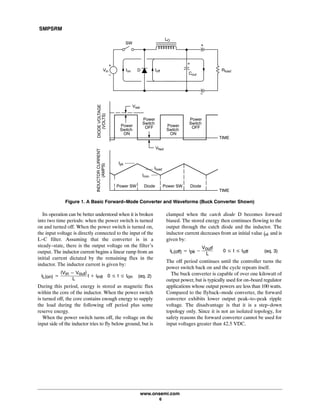
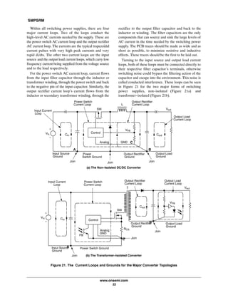
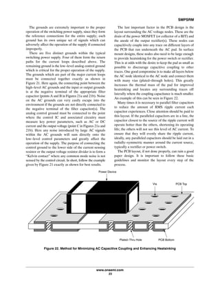
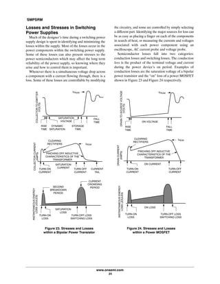
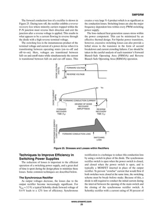


This document provides a summary of information about switching power supplies. It begins with an introduction comparing linear and switching power supplies. The main sections describe switching power supply fundamentals, common topologies, control methods, component selection, techniques to improve efficiency, and examples. Integrated circuits and components for designing switching power supplies are also listed.


![Fundamentals of power electronics [presentation slides] 2nd ed r. erickson ww](https://cdn.slidesharecdn.com/ss_thumbnails/fundamentalsofpowerelectronicspresentationslides2nded-r-ericksonww-100522135011-phpapp02-thumbnail.jpg?width=640&height=640&fit=bounds)