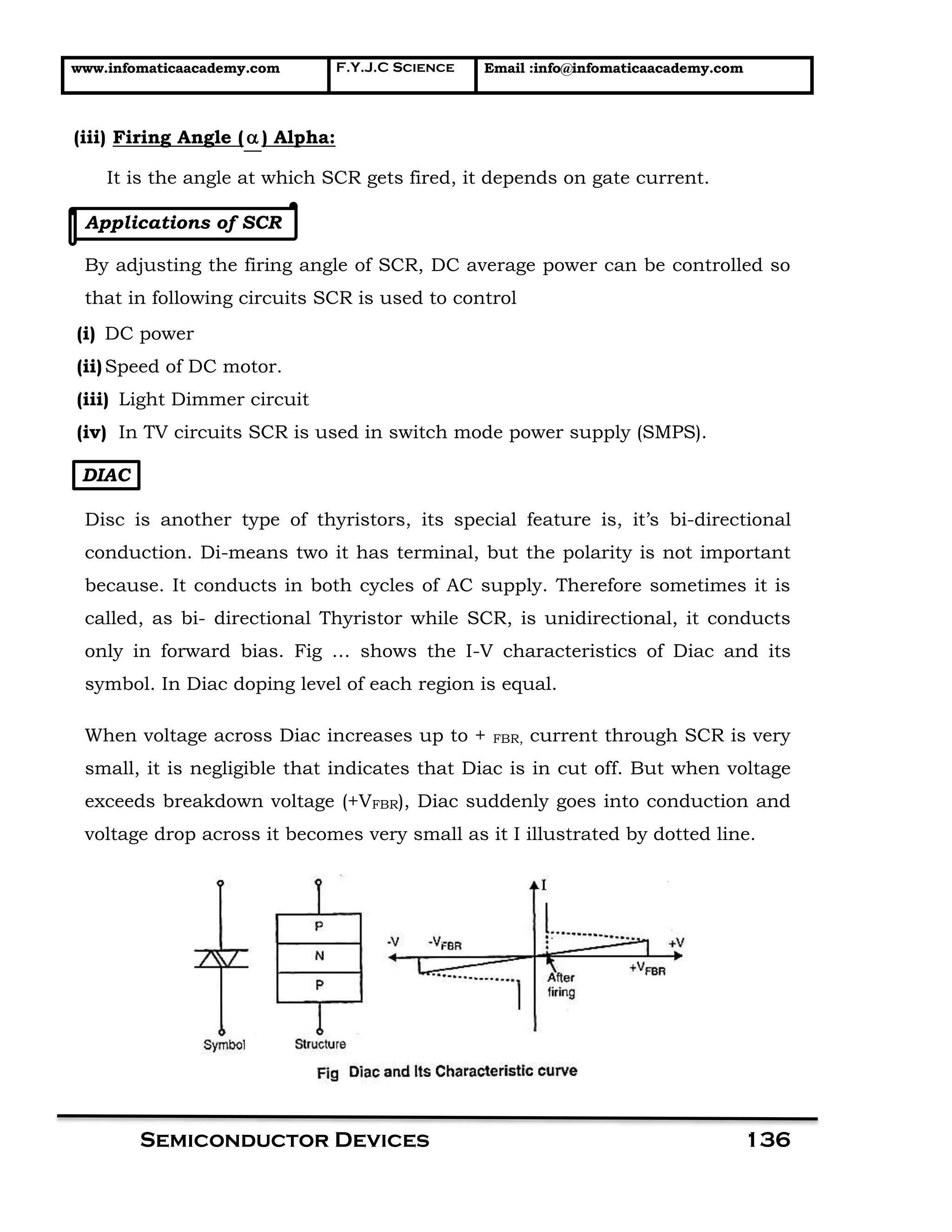
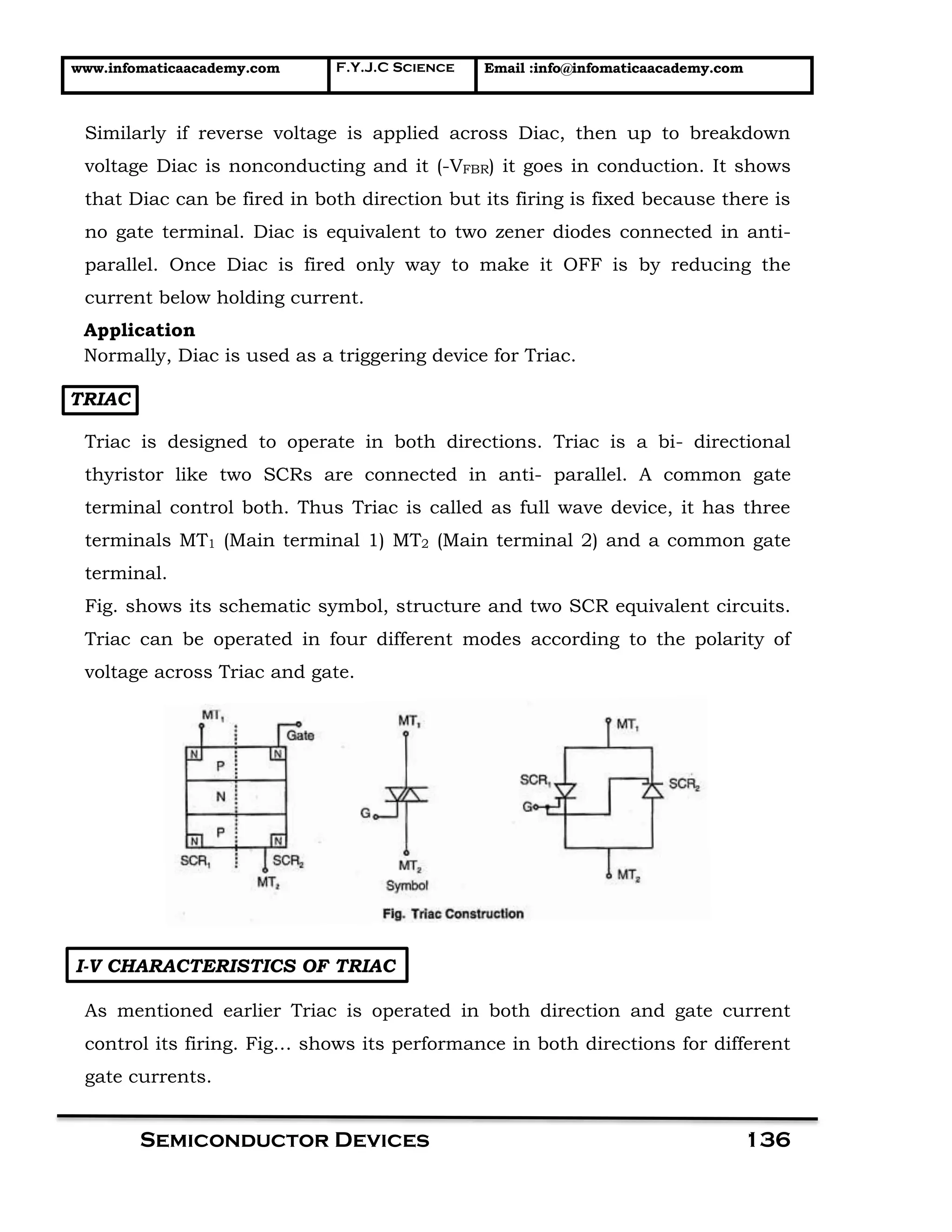
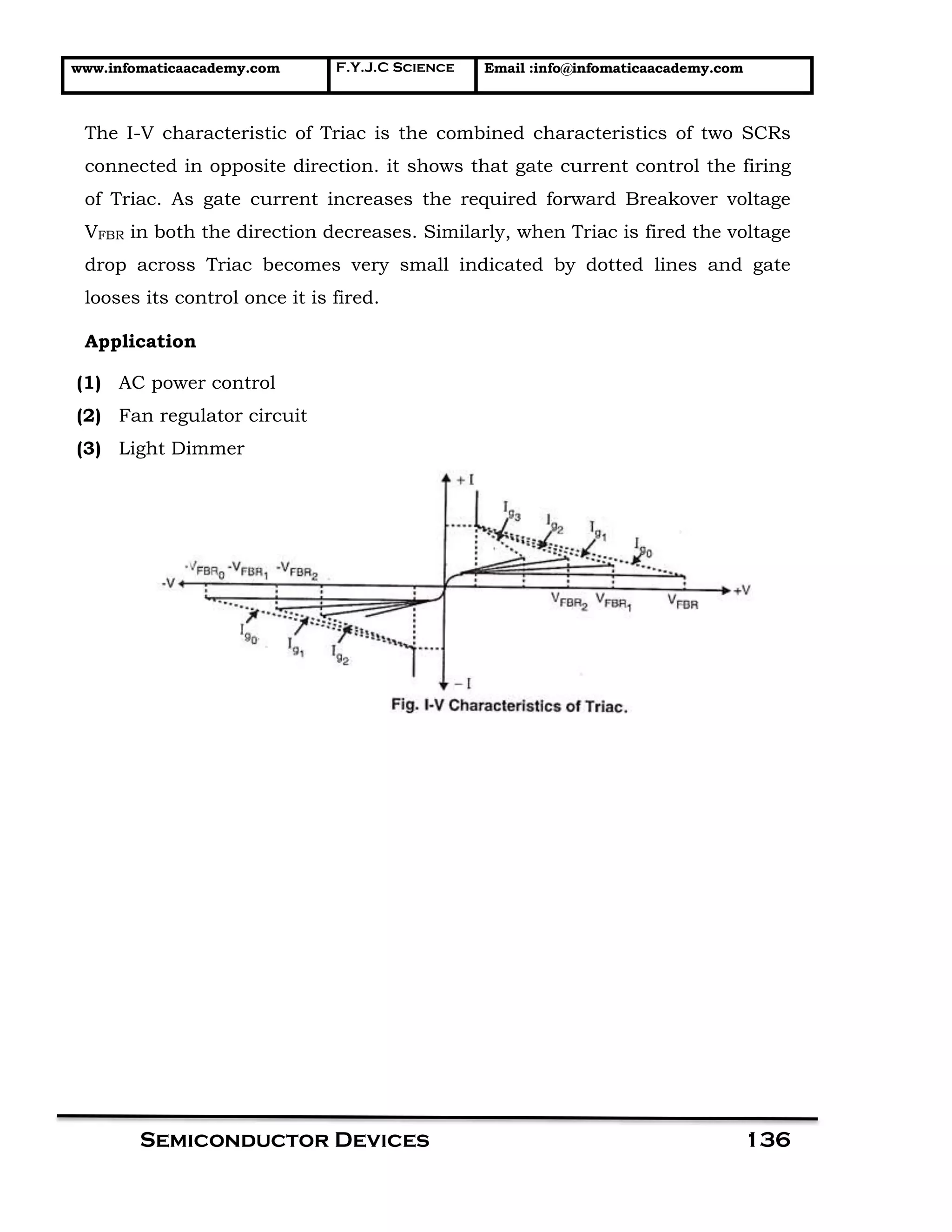
www.infomaticaacademy.com F.Y.J.C Science Email :info@infomaticaacademy.com
Semiconductor Devices 136
SEMICONDUCTOR DIODES
In addition to rectifier diode there are other kinds of semiconductor diodes,
which are manufactured for special applications are:
1) Zener diode 2) Light emitting diode (LED) 3) Photo-diode
4) Varactor diode 5) Schottkey diode 6) Tunnel diode
Let us see their structures, symbols and applications in brief.
1) Zener Diode
Zener Diode is designed to get stable voltage and it is operated in reverse
bias only. By adjusting the doping level, zener diodes of different voltages
from 2 to 200V and with different wattage are manufactured. Fig. shows
it’s operating I – V characteristics, a simple zener regular and its symbol.
The Zener gives useful working in bias only. In forward bias it conducts
just rectifier diode, it is therefore very important to know about its reverse
characteristics.
As Shown in the fig a reverse bias voltage is applied across. Initially, as
voltage across zener increases the current through zener is very small and
at a particular voltage ( )zV zener goes into breakdown. At this voltage
current through zener suddenly increases but voltage across it remains
constant. For further increase in voltage zener keeps voltage across it
constant and it draws more current through itsel. Below ( min)zI current,
Semiconductor Devices
www.infomaticaacademy.com F.Y.J.C Science Email :info@infomaticaacademy.com
Semiconductor Devices 136
zener is not operated and above ( max)zI it may get damaged. Zener should
be operated in between zI min and zI max.
Avalanche and Zener effect
A large Current through zener at breakdown is because of these two
effects. In zener effect; when voltage is breakdown voltage or more, large
number of electron hole pairs are generated because they are pulled from
covalent bonds therefore current suddenly increase this is called as ‘zener
effect’.
In avalanche effect; because of reverse applied voltage minority current
carriers are accelerated in the depletion layer. When they are accelerated,
collisions with other atoms take place. This generates new electrons,
which are again accelerated, so more atoms get ionised and thus a bunch
of electrons or a avalanche of electrons is produced which increases the
reverse current through zener. This is called as ‘avalanche effect’ we get
zener diode characteristics because of both effects. Zener Diodes are
available in different voltages and wattage e.g. 7.4V/1W, 6V/2W,
24V/2Wetc.
Applications
Zener diode is used in DC power supplies as a voltage regulator or in
special circuits to stabilize the voltage.
ZENER REGULATOR
Zener diode is used for voltage regulation; it keeps voltage constant when
there is change in input voltage within certain limit. It also keeps voltage
constant when there is change in load current within certain limit.
Following example shows its regulation action.
www.infomaticaacademy.com F.Y.J.C Science Email :info@infomaticaacademy.com
Semiconductor Devices 136
Example
Suppose required output voltage is 15 V and if there is change in input
voltage from 19 to 22 volts. The value of Rs is calculated; suppose it is 200
 and zener is 15 V/1W.
Case 1
If Vin = 20 V then current through zener is suppose 25 milliamp therefore
voltage drop across series resistance Rs will be
Case 2
Now suppose Vin increases to 22 V as we. Know current through zener will
increase from 25 mA to 35 mA. Now voltage drop across Rs will be
RS z sV = I ×R V Vin V
=35mA 200 7V =22V - 7V =15V
RS  
 
Case 3
Let us consider decrease in supply to 19 V. Now current through zener will
decrease from 35 mA to 20mA
RS z s RSV = I ×R V Vin - V
=20mA 200 = 4V =19 V - 4 V = 15 V
 

2) Light Emitting Diode (LED)
This diode plays an important role in indicators and displays. LED is
prepared with gallium (Ga), arsenic (As) and phosphorus (p). When light –
emitting diode is in forward bias it emits light instead of heat generated by
RS z s
0 in RS
V = I ×R
= 25 mA 200 = 5 V
V V V = 20 V 5 V = 15 V

   
www.infomaticaacademy.com F.Y.J.C Science Email :info@infomaticaacademy.com
Semiconductor Devices 136
a normal diode. When P-N junction is forward biased in case of L.E.D
some of the holes combine with electrons of N-region and some of the
electrons from N combine with holes of P-region. Each recombination
radiates light or photos. LED’s are available in three colours Red, Green &
Yellow. Their working voltage drop is 1 to 2 V and current is 5 to 25 mA.
Applications
They are used in 7 segment displays as panel indicators, in watches,
calculators, digital meters and as a switch –ON indicators on power supply
panels. A series resistance is always required with LED to limit the current
because if excess current flows through it, LED may get damaged. (The
value of resistance is calculated by ohms law R = V/I).
3) Photo Diode
The function of this diode is opposite to LED, when light is incident on it,
it conducts. It is manufactured with cadmium Selenide (CdSe), cadmium
cadmium sulphide (Cds) in addition to germanium and silicon. Fig. shows
its symbol. The current through photodiode depends on the light intensity.
Photo-diode is normally operated in reverse bias. When it is exposed to
light due of energy of light, electron-hole pairs are generated therefore
current flows through it. Photodiode is a transducer converts light energy
into electrical energy.
www.infomaticaacademy.com F.Y.J.C Science Email :info@infomaticaacademy.com
Semiconductor Devices 136
Applications
In computer punch card; light detectors, sound reproduction of film
projector and light operated switches.
COMPARISON
LED Photo Diode
1. It emits light when
conducts.
2. It is operated in
forward bias.
3. Symbol
4. Light intensity depends
on current
through it.
5. Used as indicators or
displays.
6. Material used Gallium,
Arsenic Phosphorus.
1. It conducts when light
is incident on it.
2. It is operated in
reverse bias.
3. Symbol
4. Current through it
depends on
light intensity.
5. Used as light sensor or
transducer.
6. Cadmium selenide,
admium Sulphide.
4) Varactor Diode
Varactor means (variable capacitance) whose junction capacitance varies
with applied reverse bias voltage. In this diode P-N junction acts two
parallel plates and potential barrier as a dielectric. As we have discussed
earlier the width of potential barrier varies with applied reverse bias
therefore the distance between two plates varies.
This variation will change its equivalent capacitance. The symbol of
varactor diode shows its junction capacitance. Mechanically tuned
capacitors can be replaced these varactor diodes. Varactor diode in parallel
with an inductor can form a tuned circuit.
www.infomaticaacademy.com F.Y.J.C Science Email :info@infomaticaacademy.com
Semiconductor Devices 136
Applications
Varactor diodes are used in tuned circuits and in FM modulator circuit.
5) Tunnel Diode
This is a special type of diode manufactured with Silicon, Germanium,
Gallium, Arsenide and Sallium Antimony. Tunnel diode shows negative
resistance characteristics like diode, and therefore it is used as a switch.
Application
It is used in amplifiers and in very high frequency oscillators.
6) Schottkey Diode
The operation of Schottkey diode is similar to ordinary P-N diode but the
voltage drop across Schottkey diode is much less than that of P-N diode
the schottkey diode is manufactured with metal- semiconductor junction.
Advantages of schottkey diode is its fast switching action it takes very
small time to switch from ON to OFF to ON state than ordinary P-N Diode.
Applications
In digital IC’s, detectors and frequency mixers.
THYRISTORS
Thyristor name is originated from old glass tube device thyratron. Since the
working principle is similar to thyratron these semiconductor devices are
called as “solid state thyratrons” or simply thyristors. These are many
thyristors, so a separate family of these devices is formed. Thyristors are
www.infomaticaacademy.com F.Y.J.C Science Email :info@infomaticaacademy.com
Semiconductor Devices 136
being commonly used in power control circuits, which are called as power
devices.
Features of Thyristors
i) These are solid- state semiconductor control devices.
ii) There are more than two P-N junctions.
iii) They are operated in switching applications.
iv) Large power handling capacity, high cost, but size is comparatively
small.
v) They can be operated with high AC – DC voltage and with large current.
SCR – SILICON CONTROLLED RECTIFIER
Silicon controlled rectifier is a four layer P – N – P – N solid state thyratron
which has three electrons anode, cathode and gate. SCR is basically is diode
but it differs from normal diode because
i) In SCR control rectification is possible by gate current but in normal
diode there is no gate terminal; diode conducts at 0.6 V or 0.3 V.
ii) In SCR four semiconductor regions are used, while in case of normal
diode only two.
iii) SCR has three junctions while diode only one.
iv) SCR can handle very large current than normal diode.
Fig. shows it’s symbol, construction and I–V characteristics curves.
www.infomaticaacademy.com F.Y.J.C Science Email :info@infomaticaacademy.com
Semiconductor Devices 136
Operation
SCR is used in rectifier circuits to control DC power to the load. When
forward bias voltage is applied across SCR it’s switching ON state depends
on the gate current and (V )FBR forward break over voltage.
i) If gI = 0 or gate is open and forward bias voltage ( )FV is applied across it
then as shown in fig. initially current through SCR is very small which is
due to minority carriers called as leaked current. The leakage current
flows up to particular voltage, but at a very high voltage FBRV , SCR
suddenly goes into conduction. Refer I – V characteristics, it is shown by a
dotted line current through SCR suddenly increases the SCR is to be fired.
The dotted line also shows that the voltage drop across it very low.
ii) If now gate current is increased gl(I ) SCR gets fired earlier, refer fig. it is
fired at FBR1V , which is less than FBRV .
iii)As gate current increases, for 2Ig SCR is fired gate loses its control on SCR,
even if gate current is made zero SCR does not change its state. Only way
to make SCR OFF is either makes voltage across it zero or apply reverse
bias. Once SCR is made ON, current through SCR must be above
particular current called as “holding current.” Let us see specifications of
SCR.
(i) Forward Breakover Voltage (VFBR)
It is the forward breakdown voltage at which SCR suddenly goes into
conduction or SCR gets fired. VFBR depends on the gate current magnitude.
(ii)Holding current (IH):
It is the minimum required current through SCR to keep SCR into ON
state. If current through SCR goes below holding current then SCR
become OFF.
www.infomaticaacademy.com F.Y.J.C Science Email :info@infomaticaacademy.com
Semiconductor Devices 136
(iii) Firing Angle () Alpha:
It is the angle at which SCR gets fired, it depends on gate current.
Applications of SCR
By adjusting the firing angle of SCR, DC average power can be controlled so
that in following circuits SCR is used to control
(i) DC power
(ii)Speed of DC motor.
(iii) Light Dimmer circuit
(iv) In TV circuits SCR is used in switch mode power supply (SMPS).
DIAC
Disc is another type of thyristors, its special feature is, it’s bi-directional
conduction. Di-means two it has terminal, but the polarity is not important
because. It conducts in both cycles of AC supply. Therefore sometimes it is
called, as bi- directional Thyristor while SCR, is unidirectional, it conducts
only in forward bias. Fig … shows the I-V characteristics of Diac and its
symbol. In Diac doping level of each region is equal.
When voltage across Diac increases up to + FBR, current through SCR is very
small, it is negligible that indicates that Diac is in cut off. But when voltage
exceeds breakdown voltage (+VFBR), Diac suddenly goes into conduction and
voltage drop across it becomes very small as it I illustrated by dotted line.
www.infomaticaacademy.com F.Y.J.C Science Email :info@infomaticaacademy.com
Semiconductor Devices 136
Similarly if reverse voltage is applied across Diac, then up to breakdown
voltage Diac is nonconducting and it (-VFBR) it goes in conduction. It shows
that Diac can be fired in both direction but its firing is fixed because there is
no gate terminal. Diac is equivalent to two zener diodes connected in anti-
parallel. Once Diac is fired only way to make it OFF is by reducing the
current below holding current.
Application
Normally, Diac is used as a triggering device for Triac.
TRIAC
Triac is designed to operate in both directions. Triac is a bi- directional
thyristor like two SCRs are connected in anti- parallel. A common gate
terminal control both. Thus Triac is called as full wave device, it has three
terminals MT1 (Main terminal 1) MT2 (Main terminal 2) and a common gate
terminal.
Fig. shows its schematic symbol, structure and two SCR equivalent circuits.
Triac can be operated in four different modes according to the polarity of
voltage across Triac and gate.
I-V CHARACTERISTICS OF TRIAC
As mentioned earlier Triac is operated in both direction and gate current
control its firing. Fig… shows its performance in both directions for different
gate currents.
www.infomaticaacademy.com F.Y.J.C Science Email :info@infomaticaacademy.com
Semiconductor Devices 136
The I-V characteristic of Triac is the combined characteristics of two SCRs
connected in opposite direction. it shows that gate current control the firing
of Triac. As gate current increases the required forward Breakover voltage
VFBR in both the direction decreases. Similarly, when Triac is fired the voltage
drop across Triac becomes very small indicated by dotted lines and gate
looses its control once it is fired.
Application
(1) AC power control
(2) Fan regulator circuit
(3) Light Dimmer

Electrical and Electronics Engineering

  • 1.
    www.infomaticaacademy.com F.Y.J.C ScienceEmail :info@infomaticaacademy.com Semiconductor Devices 136 SEMICONDUCTOR DIODES In addition to rectifier diode there are other kinds of semiconductor diodes, which are manufactured for special applications are: 1) Zener diode 2) Light emitting diode (LED) 3) Photo-diode 4) Varactor diode 5) Schottkey diode 6) Tunnel diode Let us see their structures, symbols and applications in brief. 1) Zener Diode Zener Diode is designed to get stable voltage and it is operated in reverse bias only. By adjusting the doping level, zener diodes of different voltages from 2 to 200V and with different wattage are manufactured. Fig. shows it’s operating I – V characteristics, a simple zener regular and its symbol. The Zener gives useful working in bias only. In forward bias it conducts just rectifier diode, it is therefore very important to know about its reverse characteristics. As Shown in the fig a reverse bias voltage is applied across. Initially, as voltage across zener increases the current through zener is very small and at a particular voltage ( )zV zener goes into breakdown. At this voltage current through zener suddenly increases but voltage across it remains constant. For further increase in voltage zener keeps voltage across it constant and it draws more current through itsel. Below ( min)zI current, Semiconductor Devices
  • 2.
    www.infomaticaacademy.com F.Y.J.C ScienceEmail :info@infomaticaacademy.com Semiconductor Devices 136 zener is not operated and above ( max)zI it may get damaged. Zener should be operated in between zI min and zI max. Avalanche and Zener effect A large Current through zener at breakdown is because of these two effects. In zener effect; when voltage is breakdown voltage or more, large number of electron hole pairs are generated because they are pulled from covalent bonds therefore current suddenly increase this is called as ‘zener effect’. In avalanche effect; because of reverse applied voltage minority current carriers are accelerated in the depletion layer. When they are accelerated, collisions with other atoms take place. This generates new electrons, which are again accelerated, so more atoms get ionised and thus a bunch of electrons or a avalanche of electrons is produced which increases the reverse current through zener. This is called as ‘avalanche effect’ we get zener diode characteristics because of both effects. Zener Diodes are available in different voltages and wattage e.g. 7.4V/1W, 6V/2W, 24V/2Wetc. Applications Zener diode is used in DC power supplies as a voltage regulator or in special circuits to stabilize the voltage. ZENER REGULATOR Zener diode is used for voltage regulation; it keeps voltage constant when there is change in input voltage within certain limit. It also keeps voltage constant when there is change in load current within certain limit. Following example shows its regulation action.
  • 3.
    www.infomaticaacademy.com F.Y.J.C ScienceEmail :info@infomaticaacademy.com Semiconductor Devices 136 Example Suppose required output voltage is 15 V and if there is change in input voltage from 19 to 22 volts. The value of Rs is calculated; suppose it is 200  and zener is 15 V/1W. Case 1 If Vin = 20 V then current through zener is suppose 25 milliamp therefore voltage drop across series resistance Rs will be Case 2 Now suppose Vin increases to 22 V as we. Know current through zener will increase from 25 mA to 35 mA. Now voltage drop across Rs will be RS z sV = I ×R V Vin V =35mA 200 7V =22V - 7V =15V RS     Case 3 Let us consider decrease in supply to 19 V. Now current through zener will decrease from 35 mA to 20mA RS z s RSV = I ×R V Vin - V =20mA 200 = 4V =19 V - 4 V = 15 V    2) Light Emitting Diode (LED) This diode plays an important role in indicators and displays. LED is prepared with gallium (Ga), arsenic (As) and phosphorus (p). When light – emitting diode is in forward bias it emits light instead of heat generated by RS z s 0 in RS V = I ×R = 25 mA 200 = 5 V V V V = 20 V 5 V = 15 V     
  • 4.
    www.infomaticaacademy.com F.Y.J.C ScienceEmail :info@infomaticaacademy.com Semiconductor Devices 136 a normal diode. When P-N junction is forward biased in case of L.E.D some of the holes combine with electrons of N-region and some of the electrons from N combine with holes of P-region. Each recombination radiates light or photos. LED’s are available in three colours Red, Green & Yellow. Their working voltage drop is 1 to 2 V and current is 5 to 25 mA. Applications They are used in 7 segment displays as panel indicators, in watches, calculators, digital meters and as a switch –ON indicators on power supply panels. A series resistance is always required with LED to limit the current because if excess current flows through it, LED may get damaged. (The value of resistance is calculated by ohms law R = V/I). 3) Photo Diode The function of this diode is opposite to LED, when light is incident on it, it conducts. It is manufactured with cadmium Selenide (CdSe), cadmium cadmium sulphide (Cds) in addition to germanium and silicon. Fig. shows its symbol. The current through photodiode depends on the light intensity. Photo-diode is normally operated in reverse bias. When it is exposed to light due of energy of light, electron-hole pairs are generated therefore current flows through it. Photodiode is a transducer converts light energy into electrical energy.
  • 5.
    www.infomaticaacademy.com F.Y.J.C ScienceEmail :info@infomaticaacademy.com Semiconductor Devices 136 Applications In computer punch card; light detectors, sound reproduction of film projector and light operated switches. COMPARISON LED Photo Diode 1. It emits light when conducts. 2. It is operated in forward bias. 3. Symbol 4. Light intensity depends on current through it. 5. Used as indicators or displays. 6. Material used Gallium, Arsenic Phosphorus. 1. It conducts when light is incident on it. 2. It is operated in reverse bias. 3. Symbol 4. Current through it depends on light intensity. 5. Used as light sensor or transducer. 6. Cadmium selenide, admium Sulphide. 4) Varactor Diode Varactor means (variable capacitance) whose junction capacitance varies with applied reverse bias voltage. In this diode P-N junction acts two parallel plates and potential barrier as a dielectric. As we have discussed earlier the width of potential barrier varies with applied reverse bias therefore the distance between two plates varies. This variation will change its equivalent capacitance. The symbol of varactor diode shows its junction capacitance. Mechanically tuned capacitors can be replaced these varactor diodes. Varactor diode in parallel with an inductor can form a tuned circuit.
  • 6.
    www.infomaticaacademy.com F.Y.J.C ScienceEmail :info@infomaticaacademy.com Semiconductor Devices 136 Applications Varactor diodes are used in tuned circuits and in FM modulator circuit. 5) Tunnel Diode This is a special type of diode manufactured with Silicon, Germanium, Gallium, Arsenide and Sallium Antimony. Tunnel diode shows negative resistance characteristics like diode, and therefore it is used as a switch. Application It is used in amplifiers and in very high frequency oscillators. 6) Schottkey Diode The operation of Schottkey diode is similar to ordinary P-N diode but the voltage drop across Schottkey diode is much less than that of P-N diode the schottkey diode is manufactured with metal- semiconductor junction. Advantages of schottkey diode is its fast switching action it takes very small time to switch from ON to OFF to ON state than ordinary P-N Diode. Applications In digital IC’s, detectors and frequency mixers. THYRISTORS Thyristor name is originated from old glass tube device thyratron. Since the working principle is similar to thyratron these semiconductor devices are called as “solid state thyratrons” or simply thyristors. These are many thyristors, so a separate family of these devices is formed. Thyristors are
  • 7.
    www.infomaticaacademy.com F.Y.J.C ScienceEmail :info@infomaticaacademy.com Semiconductor Devices 136 being commonly used in power control circuits, which are called as power devices. Features of Thyristors i) These are solid- state semiconductor control devices. ii) There are more than two P-N junctions. iii) They are operated in switching applications. iv) Large power handling capacity, high cost, but size is comparatively small. v) They can be operated with high AC – DC voltage and with large current. SCR – SILICON CONTROLLED RECTIFIER Silicon controlled rectifier is a four layer P – N – P – N solid state thyratron which has three electrons anode, cathode and gate. SCR is basically is diode but it differs from normal diode because i) In SCR control rectification is possible by gate current but in normal diode there is no gate terminal; diode conducts at 0.6 V or 0.3 V. ii) In SCR four semiconductor regions are used, while in case of normal diode only two. iii) SCR has three junctions while diode only one. iv) SCR can handle very large current than normal diode. Fig. shows it’s symbol, construction and I–V characteristics curves.
  • 8.
    www.infomaticaacademy.com F.Y.J.C ScienceEmail :info@infomaticaacademy.com Semiconductor Devices 136 Operation SCR is used in rectifier circuits to control DC power to the load. When forward bias voltage is applied across SCR it’s switching ON state depends on the gate current and (V )FBR forward break over voltage. i) If gI = 0 or gate is open and forward bias voltage ( )FV is applied across it then as shown in fig. initially current through SCR is very small which is due to minority carriers called as leaked current. The leakage current flows up to particular voltage, but at a very high voltage FBRV , SCR suddenly goes into conduction. Refer I – V characteristics, it is shown by a dotted line current through SCR suddenly increases the SCR is to be fired. The dotted line also shows that the voltage drop across it very low. ii) If now gate current is increased gl(I ) SCR gets fired earlier, refer fig. it is fired at FBR1V , which is less than FBRV . iii)As gate current increases, for 2Ig SCR is fired gate loses its control on SCR, even if gate current is made zero SCR does not change its state. Only way to make SCR OFF is either makes voltage across it zero or apply reverse bias. Once SCR is made ON, current through SCR must be above particular current called as “holding current.” Let us see specifications of SCR. (i) Forward Breakover Voltage (VFBR) It is the forward breakdown voltage at which SCR suddenly goes into conduction or SCR gets fired. VFBR depends on the gate current magnitude. (ii)Holding current (IH): It is the minimum required current through SCR to keep SCR into ON state. If current through SCR goes below holding current then SCR become OFF.
  • 9.
    www.infomaticaacademy.com F.Y.J.C ScienceEmail :info@infomaticaacademy.com Semiconductor Devices 136 (iii) Firing Angle () Alpha: It is the angle at which SCR gets fired, it depends on gate current. Applications of SCR By adjusting the firing angle of SCR, DC average power can be controlled so that in following circuits SCR is used to control (i) DC power (ii)Speed of DC motor. (iii) Light Dimmer circuit (iv) In TV circuits SCR is used in switch mode power supply (SMPS). DIAC Disc is another type of thyristors, its special feature is, it’s bi-directional conduction. Di-means two it has terminal, but the polarity is not important because. It conducts in both cycles of AC supply. Therefore sometimes it is called, as bi- directional Thyristor while SCR, is unidirectional, it conducts only in forward bias. Fig … shows the I-V characteristics of Diac and its symbol. In Diac doping level of each region is equal. When voltage across Diac increases up to + FBR, current through SCR is very small, it is negligible that indicates that Diac is in cut off. But when voltage exceeds breakdown voltage (+VFBR), Diac suddenly goes into conduction and voltage drop across it becomes very small as it I illustrated by dotted line.
  • 10.
    www.infomaticaacademy.com F.Y.J.C ScienceEmail :info@infomaticaacademy.com Semiconductor Devices 136 Similarly if reverse voltage is applied across Diac, then up to breakdown voltage Diac is nonconducting and it (-VFBR) it goes in conduction. It shows that Diac can be fired in both direction but its firing is fixed because there is no gate terminal. Diac is equivalent to two zener diodes connected in anti- parallel. Once Diac is fired only way to make it OFF is by reducing the current below holding current. Application Normally, Diac is used as a triggering device for Triac. TRIAC Triac is designed to operate in both directions. Triac is a bi- directional thyristor like two SCRs are connected in anti- parallel. A common gate terminal control both. Thus Triac is called as full wave device, it has three terminals MT1 (Main terminal 1) MT2 (Main terminal 2) and a common gate terminal. Fig. shows its schematic symbol, structure and two SCR equivalent circuits. Triac can be operated in four different modes according to the polarity of voltage across Triac and gate. I-V CHARACTERISTICS OF TRIAC As mentioned earlier Triac is operated in both direction and gate current control its firing. Fig… shows its performance in both directions for different gate currents.
  • 11.
    www.infomaticaacademy.com F.Y.J.C ScienceEmail :info@infomaticaacademy.com Semiconductor Devices 136 The I-V characteristic of Triac is the combined characteristics of two SCRs connected in opposite direction. it shows that gate current control the firing of Triac. As gate current increases the required forward Breakover voltage VFBR in both the direction decreases. Similarly, when Triac is fired the voltage drop across Triac becomes very small indicated by dotted lines and gate looses its control once it is fired. Application (1) AC power control (2) Fan regulator circuit (3) Light Dimmer