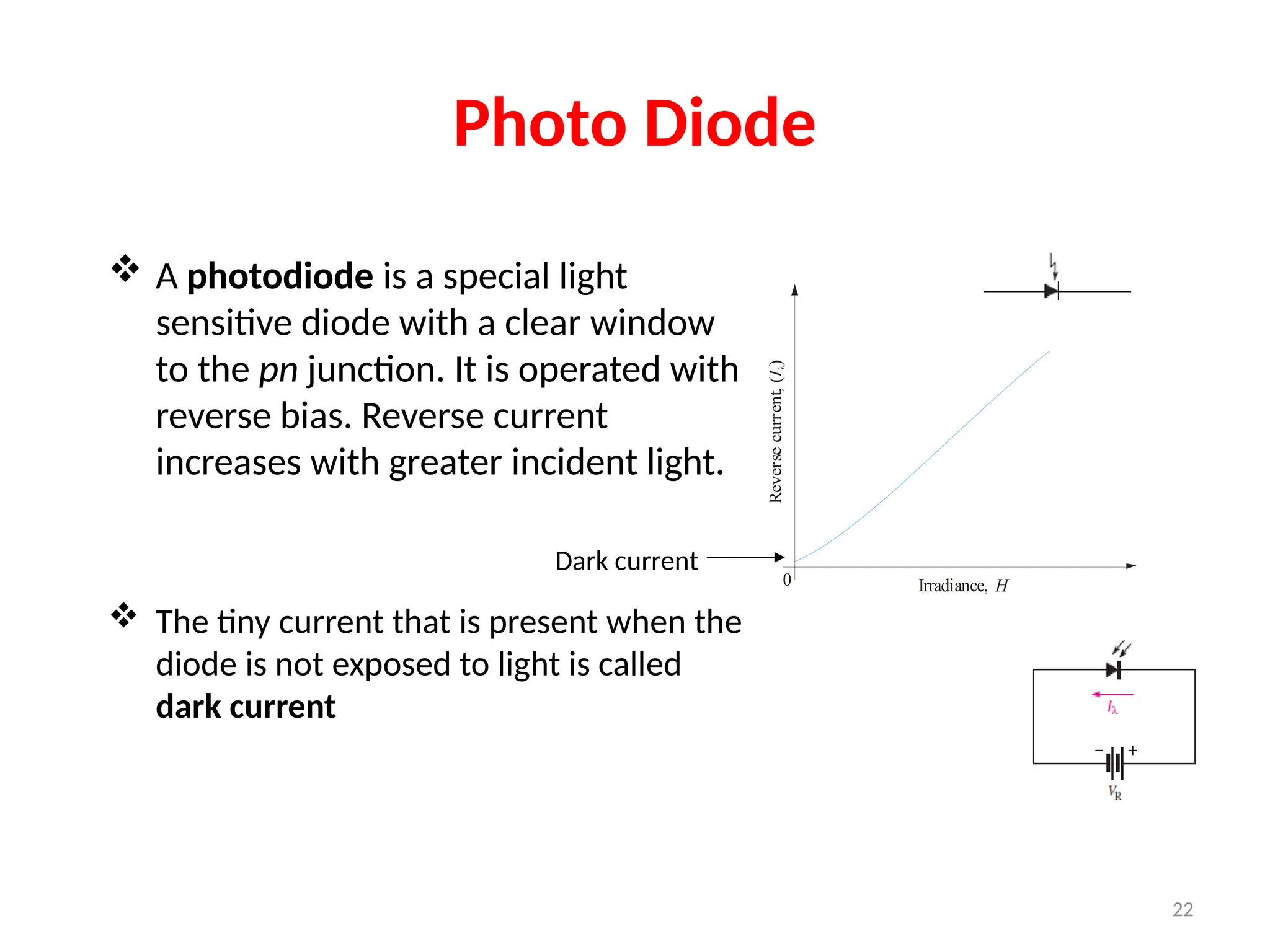
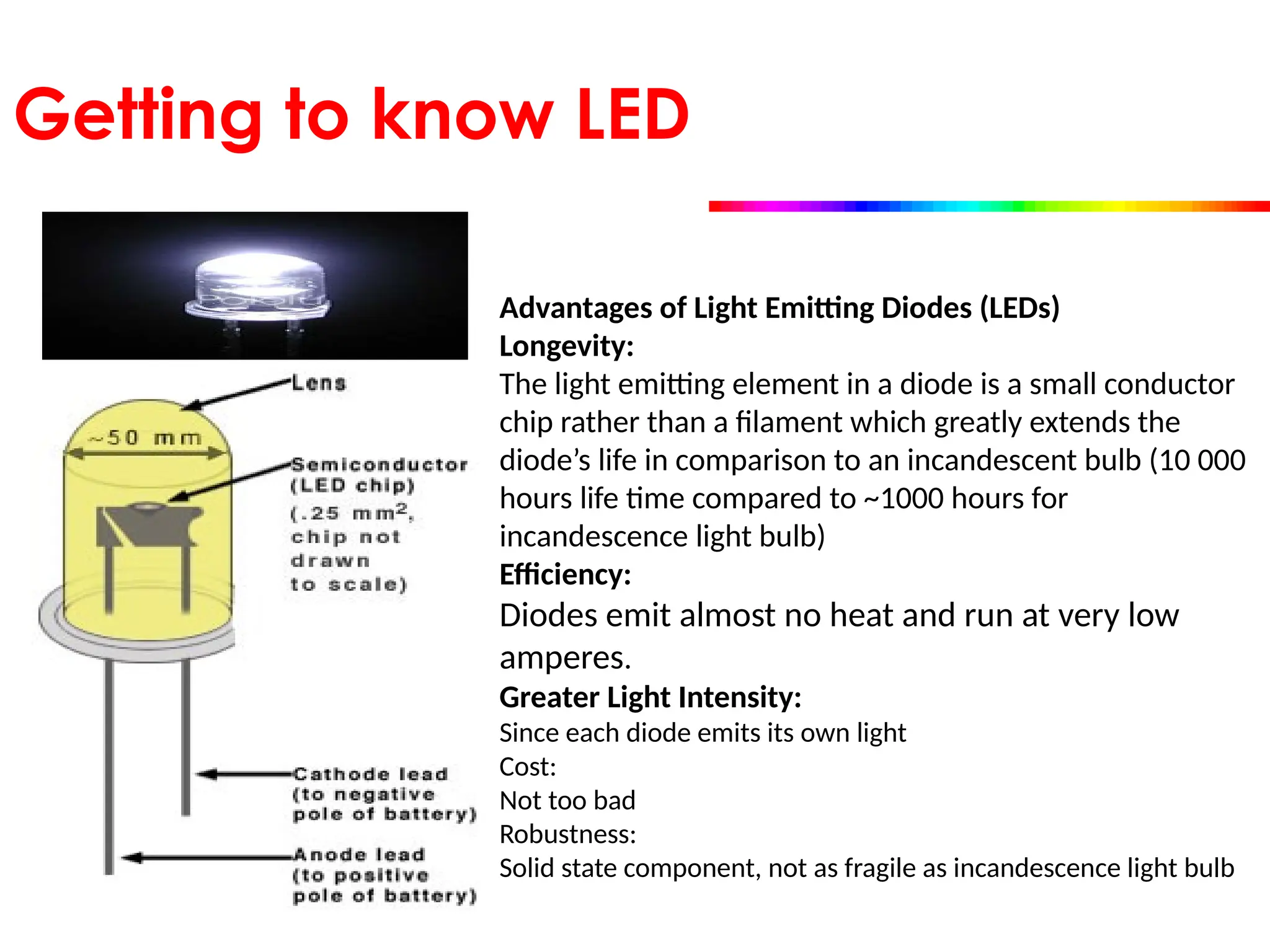
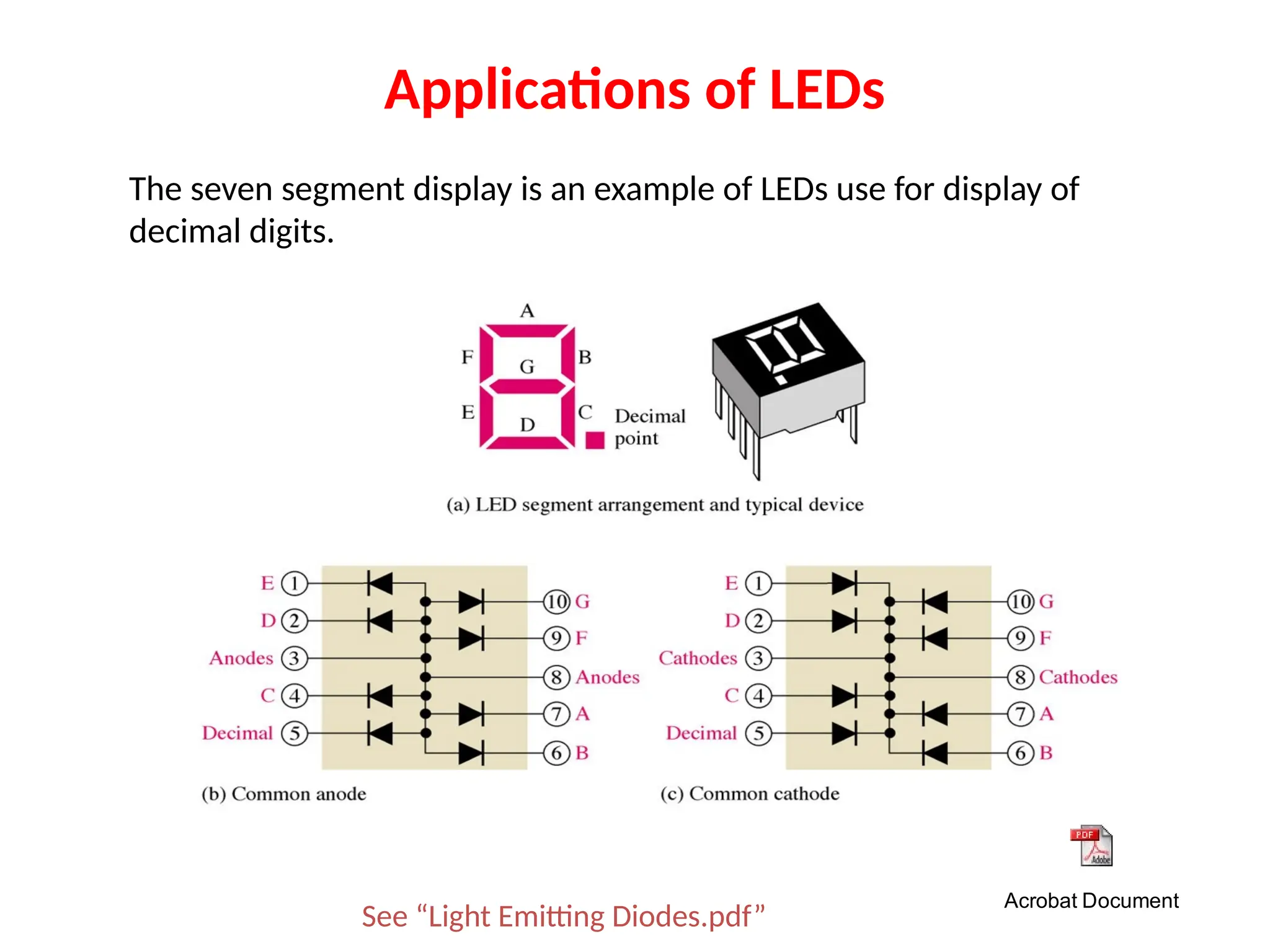
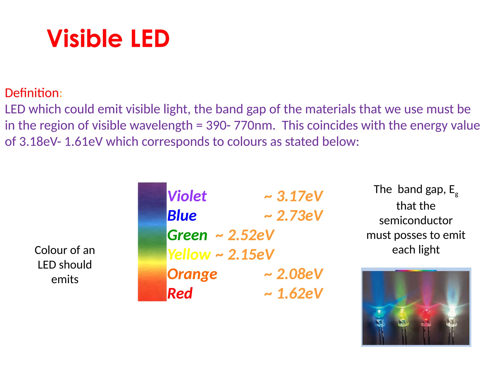
Download to read offline

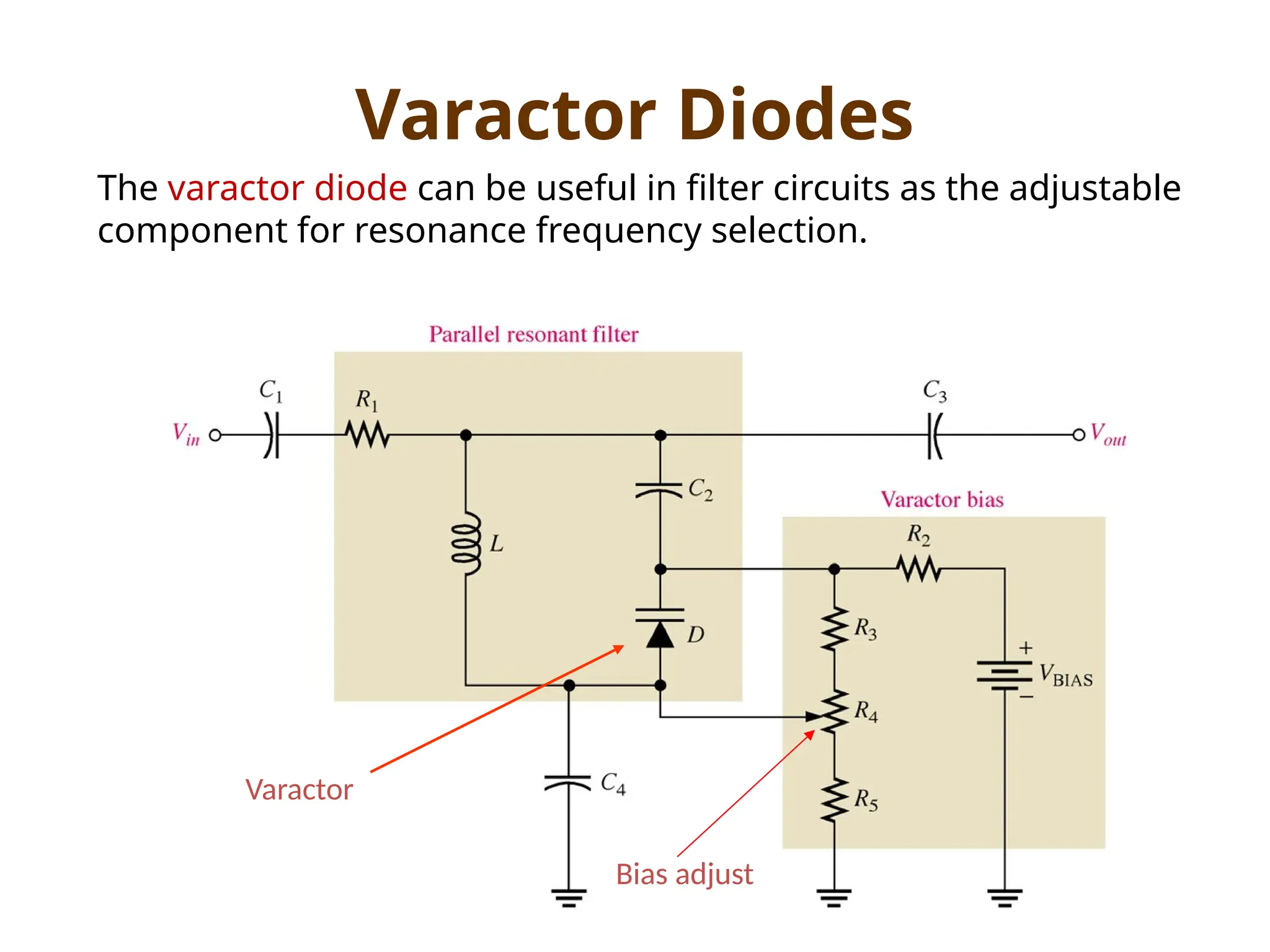
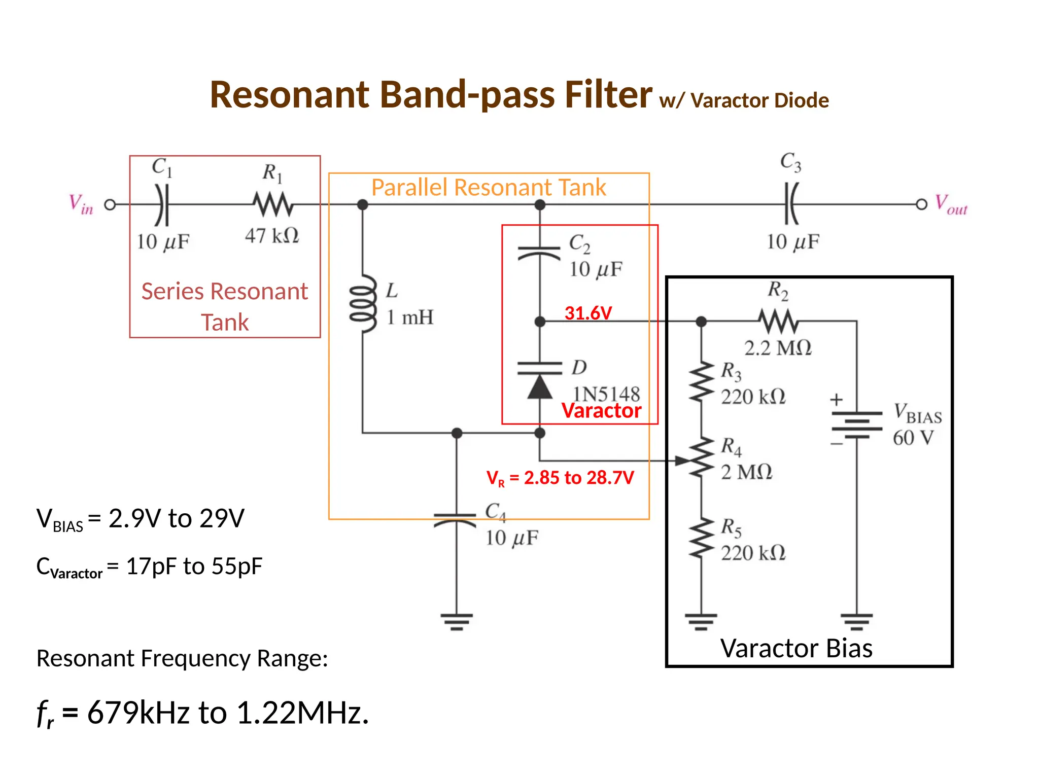
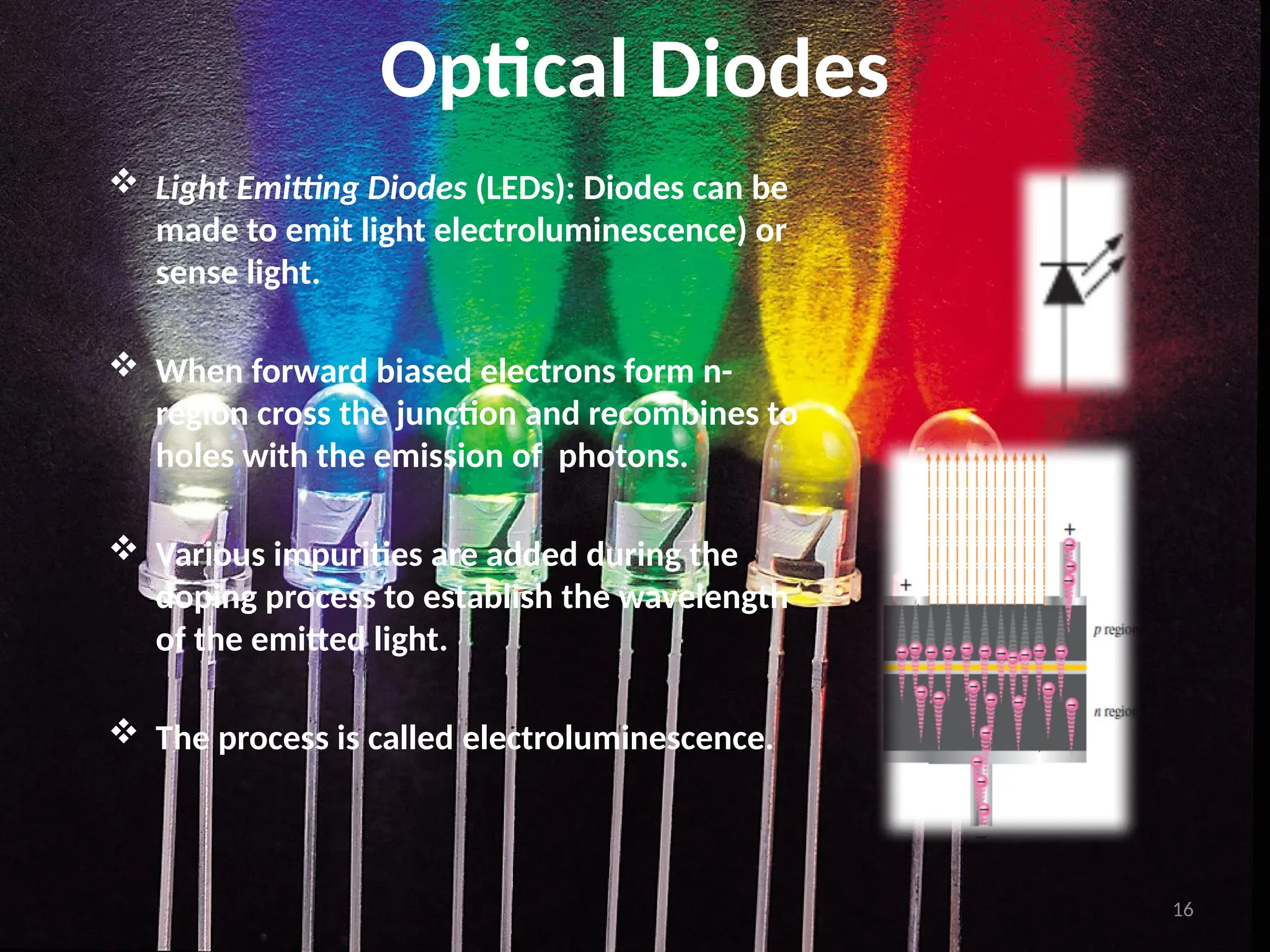
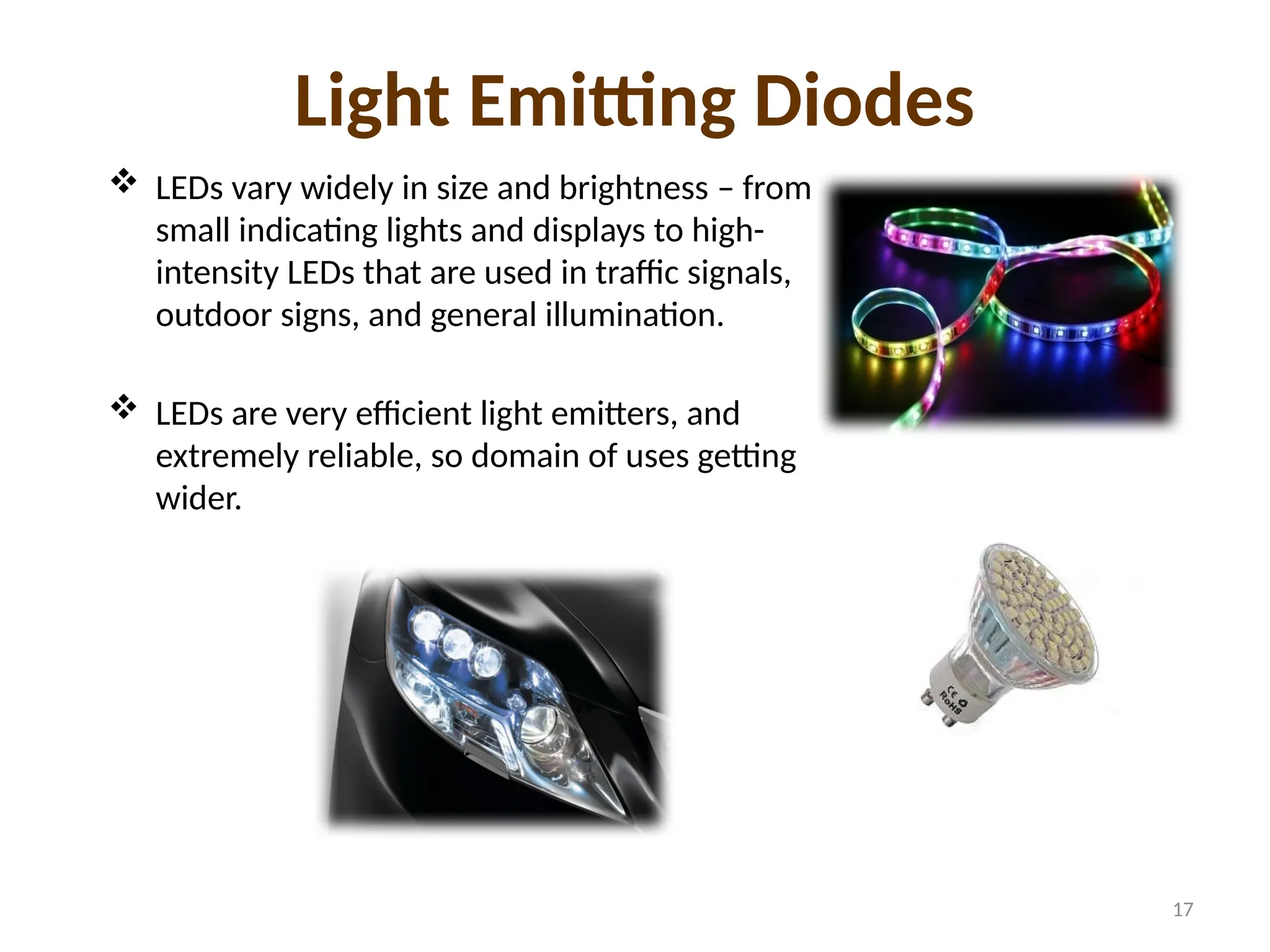


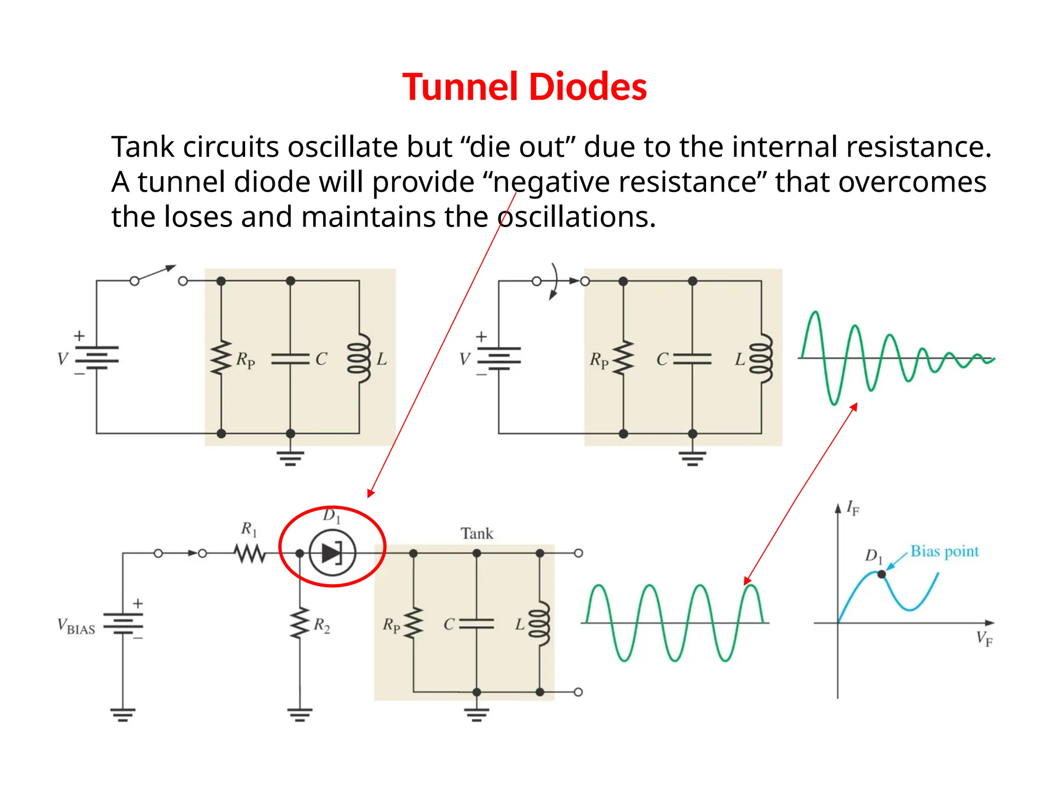


In this concise, example‑driven presentation, Dr. G.S. Virdi (Former Chief Scientist, CSIR‑Central Electronics Engineering Research Institute) explores the world of diodes—from the textbook “ideal” model to the nuances of real‑life performance, and on to a showcase of special‑purpose diodes. You’ll discover: Ideal vs. Practical Diodes: What happens when you assume zero resistance and zero voltage drop—and why real diodes always deviate Practical Considerations: Forward‑bias resistance, power dissipation limits, reverse‑bias breakdown Special‑Purpose Diode Gallery: Zener, LEDs, photodiodes, varactors, tunnel, Schottky & Shockley diodes—what sets each apart and where to use them Perfect for electronics students, hobbyists, and design engineers looking to solidify their understanding of semiconductor fundamentals. #Diodes #SemiconductorDevices #ElectronicsFundamentals #CircuitDesign


