Zener Diode
AZener Diode is a special kind of diode which permits
current to flow in the forward direction as normal, but will
also allow it to flow in the reverse direction when the
voltage is above a certain value – the breakdown voltage
known as the Zener voltage.
Zener diode consists of two terminals: CATHODE and
ANODE.
In zener diode, electric current flows from both anode to
cathode and cathode to anode.
The symbol of zener diode is similar to the normal p-n
junction diode, but with bend edges on the vertical bar.
4.
Circuit Diagram
TheZener diode is employed in reverse biasing. The
reverse biasing means the n-type material of the diode is
connected to the positive terminal of the supply and the P-
type material is connected to the negative terminal of the
supply.
The depletion region of the diode is very thin because it is
made of the heavily doped semiconductor material.
5.
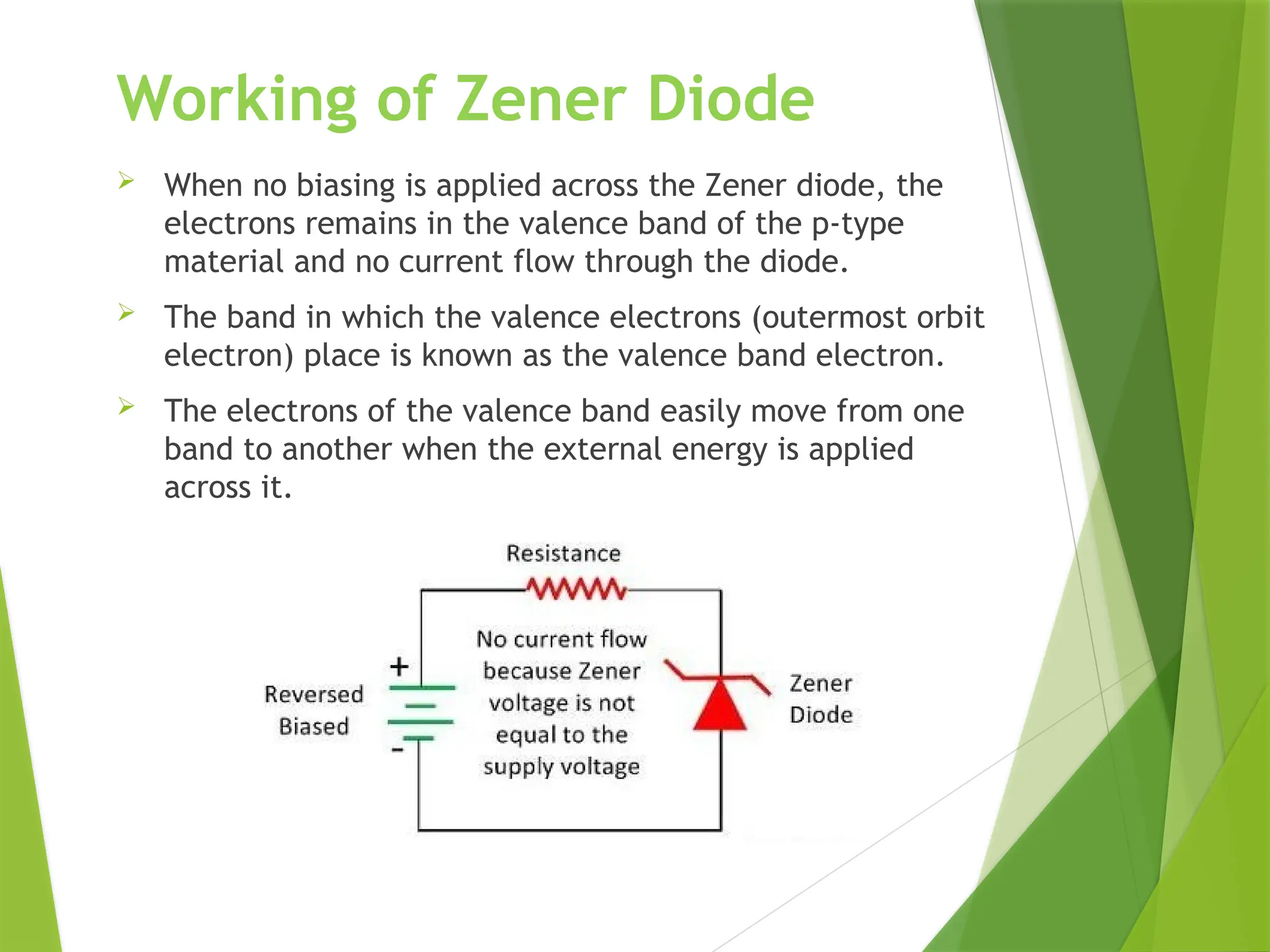
Working of ZenerDiode
When no biasing is applied across the Zener diode, the
electrons remains in the valence band of the p-type
material and no current flow through the diode.
The band in which the valence electrons (outermost orbit
electron) place is known as the valence band electron.
The electrons of the valence band easily move from one
band to another when the external energy is applied
across it.
6.
When thereverse bias applies across the diode and the supply
voltage is equal to the Zener voltage then it starts conducting in
the reverse bias direction. T
he Zener voltage is the voltage at which the depletion region
completely vanish.
The reverse bias applies across the diode increases the intensity of
electric field across the depletion region. Thus, it allows the
electrons to move from the valence band of P-type material to the
conduction band of N-type material.
This transferring of valence band electrons to the conduction band
reduces the barrier between the p and n-type material. When the
depletion region become completely vanish the diode starts
conducting in the reverse biased.
7.
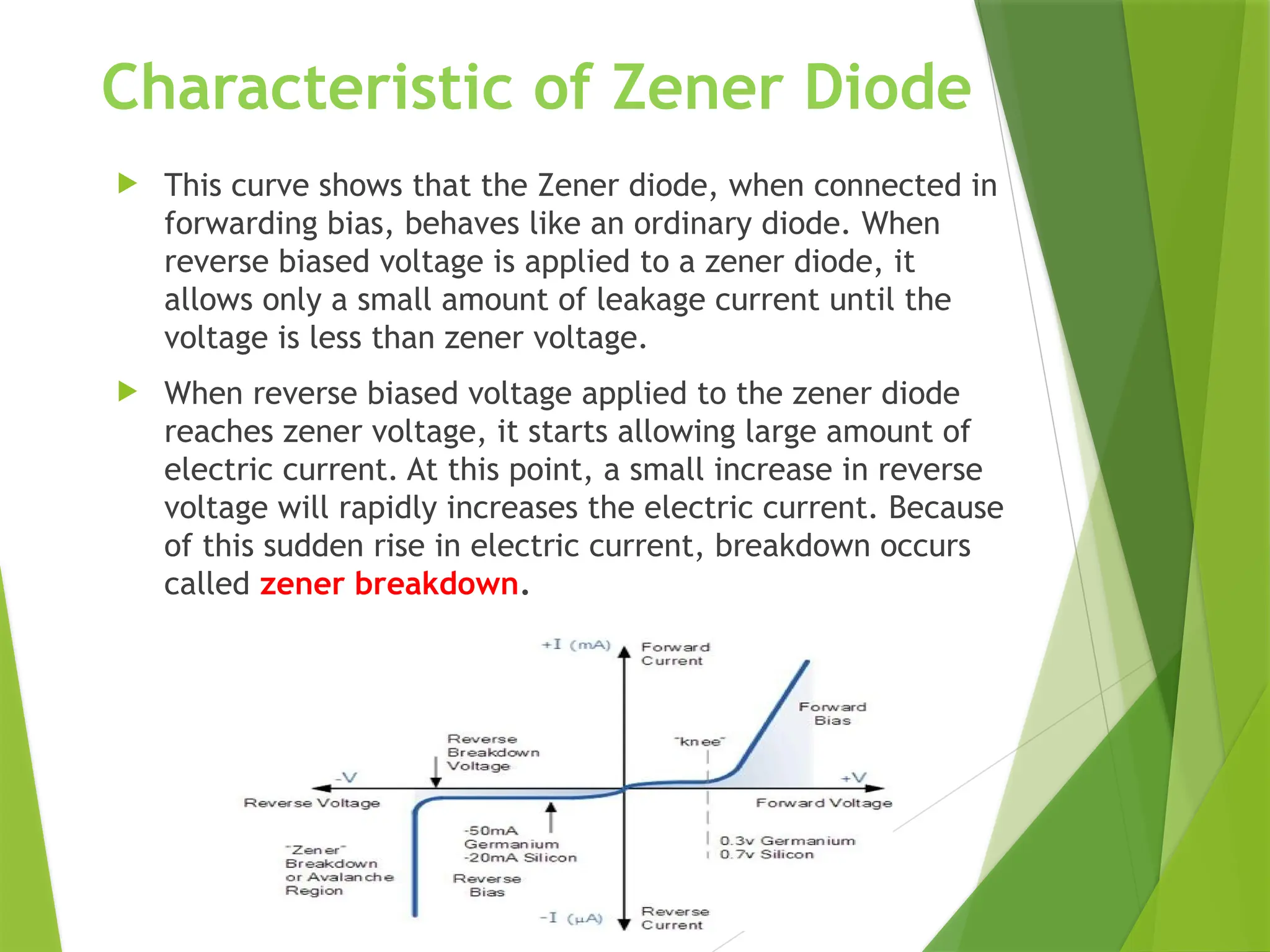
Characteristic of ZenerDiode
This curve shows that the Zener diode, when connected in
forwarding bias, behaves like an ordinary diode. When
reverse biased voltage is applied to a zener diode, it
allows only a small amount of leakage current until the
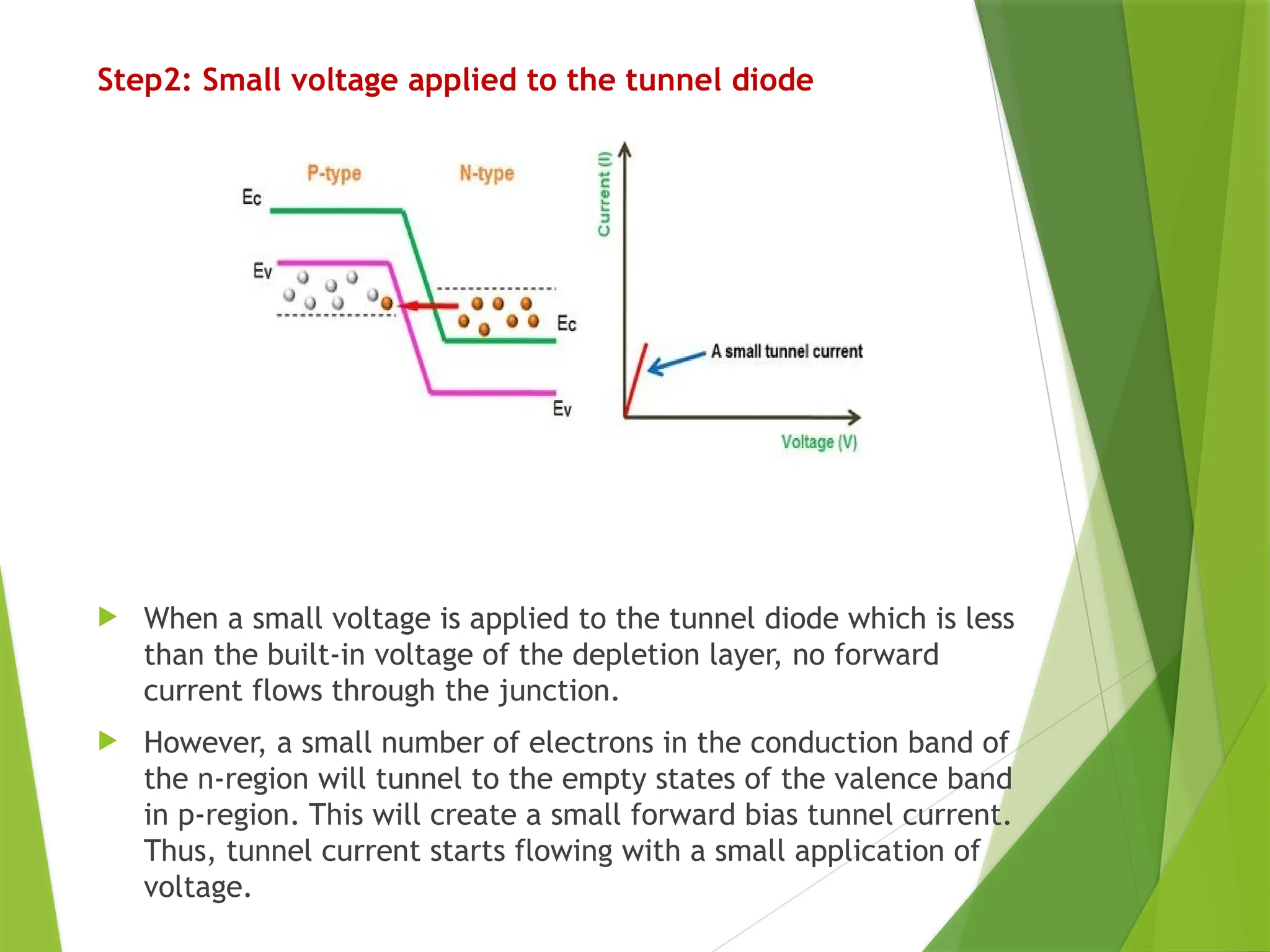
voltage is less than zener voltage.
When reverse biased voltage applied to the zener diode
reaches zener voltage, it starts allowing large amount of
electric current. At this point, a small increase in reverse
voltage will rapidly increases the electric current. Because
of this sudden rise in electric current, breakdown occurs
called zener breakdown.
8.
However, zenerdiode exhibits a controlled breakdown
that does damage the device.
The zener breakdown voltage of the zener diode is
depends on the amount of doping applied. If the diode is
heavily doped, zener breakdown occurs at low reverse
voltages.
On the other hand, if the diode is lightly doped, the
zener break down occurs at high reverse voltages.
9.
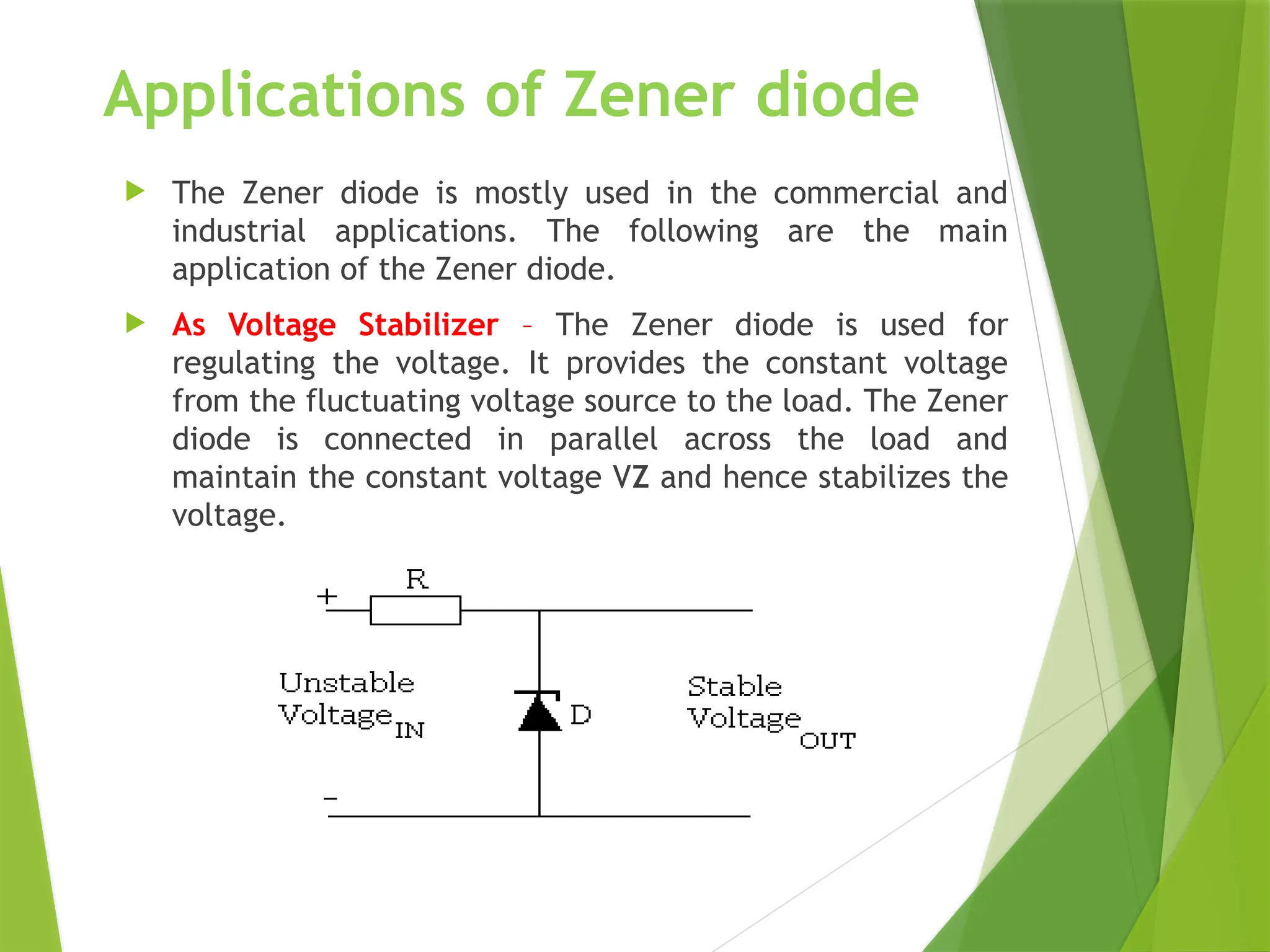
Applications of Zenerdiode
The Zener diode is mostly used in the commercial and
industrial applications. The following are the main
application of the Zener diode.
As Voltage Stabilizer – The Zener diode is used for
regulating the voltage. It provides the constant voltage
from the fluctuating voltage source to the load. The Zener
diode is connected in parallel across the load and
maintain the constant voltage VZ and hence stabilizes the
voltage.
10.
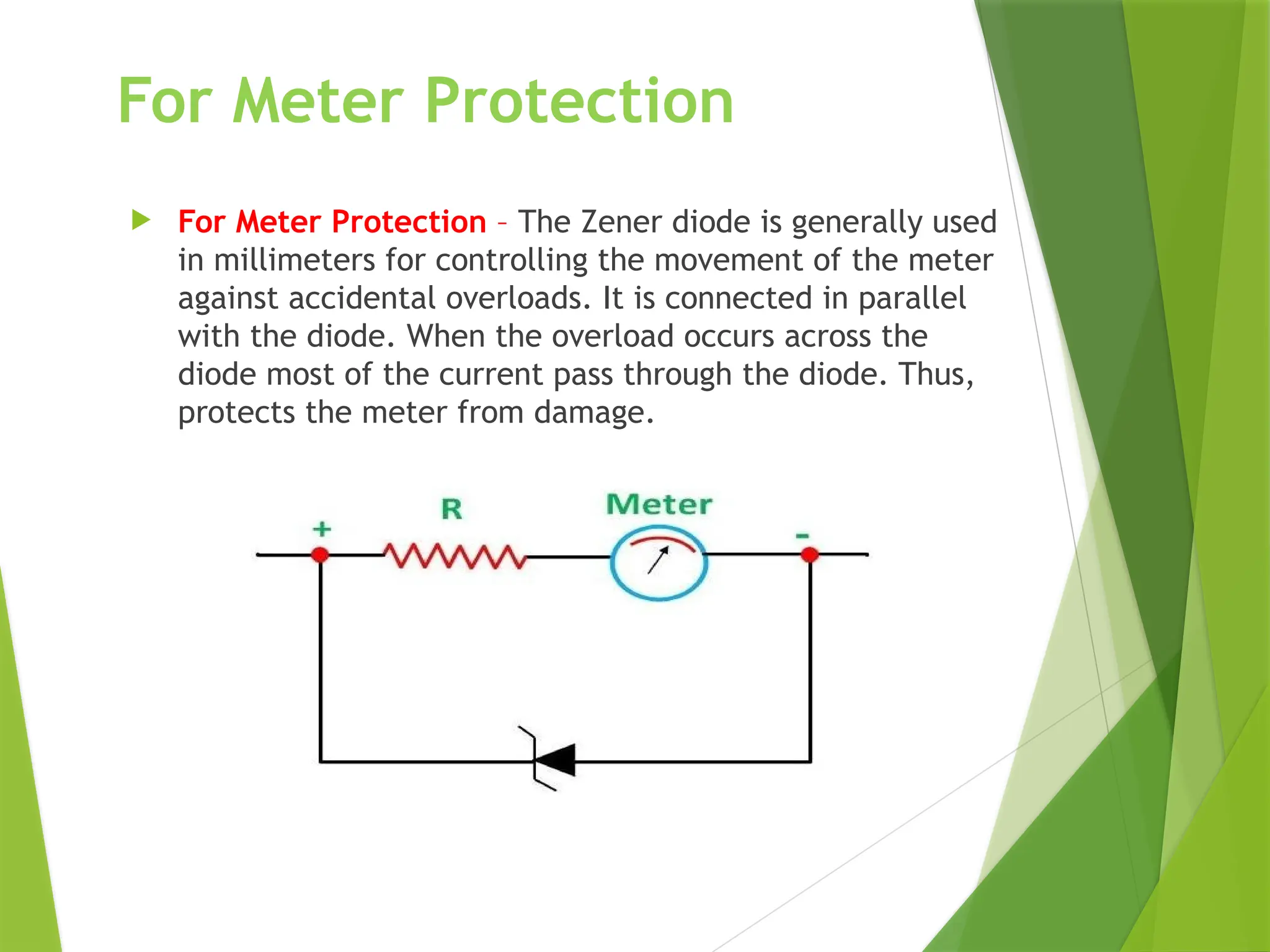
For Meter Protection
For Meter Protection – The Zener diode is generally used
in millimeters for controlling the movement of the meter
against accidental overloads. It is connected in parallel
with the diode. When the overload occurs across the
diode most of the current pass through the diode. Thus,
protects the meter from damage.
11.
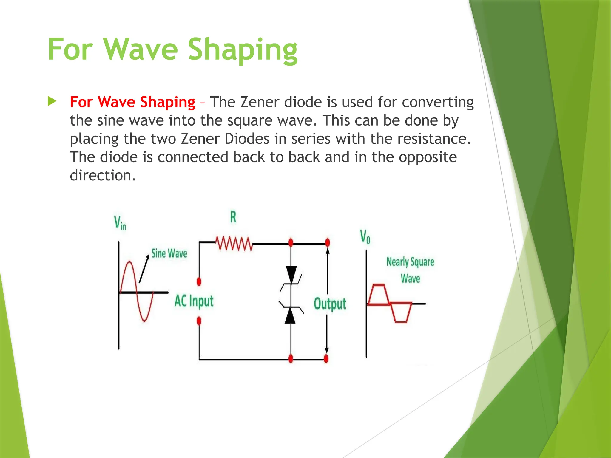
For Wave Shaping
For Wave Shaping – The Zener diode is used for converting
the sine wave into the square wave. This can be done by
placing the two Zener Diodes in series with the resistance.
The diode is connected back to back and in the opposite
direction.
12.
Difference between PNDiode &
Zener Diode
Factors
PN Junction
Diode
Zener Diode
Definition
It is a semiconductor
diode which conducts
only in one direction,
i.e., in forward
direction.
The diode which allows the
current to flow in both the
direction i.e., forward and
reverse, such type of diode
is known as the Zener
diode.
Symbol
Reverse Current
Effect
Damage the junction.
Do not damage the
junction.
Doping Level Low High
Breakdown
Occurs in higher
voltage.
Occur in lower voltage.
Ohms Law Obey Do not obey.
Applications For rectification
Voltage stabilizer, motor
protection and wave
shaping.
13.
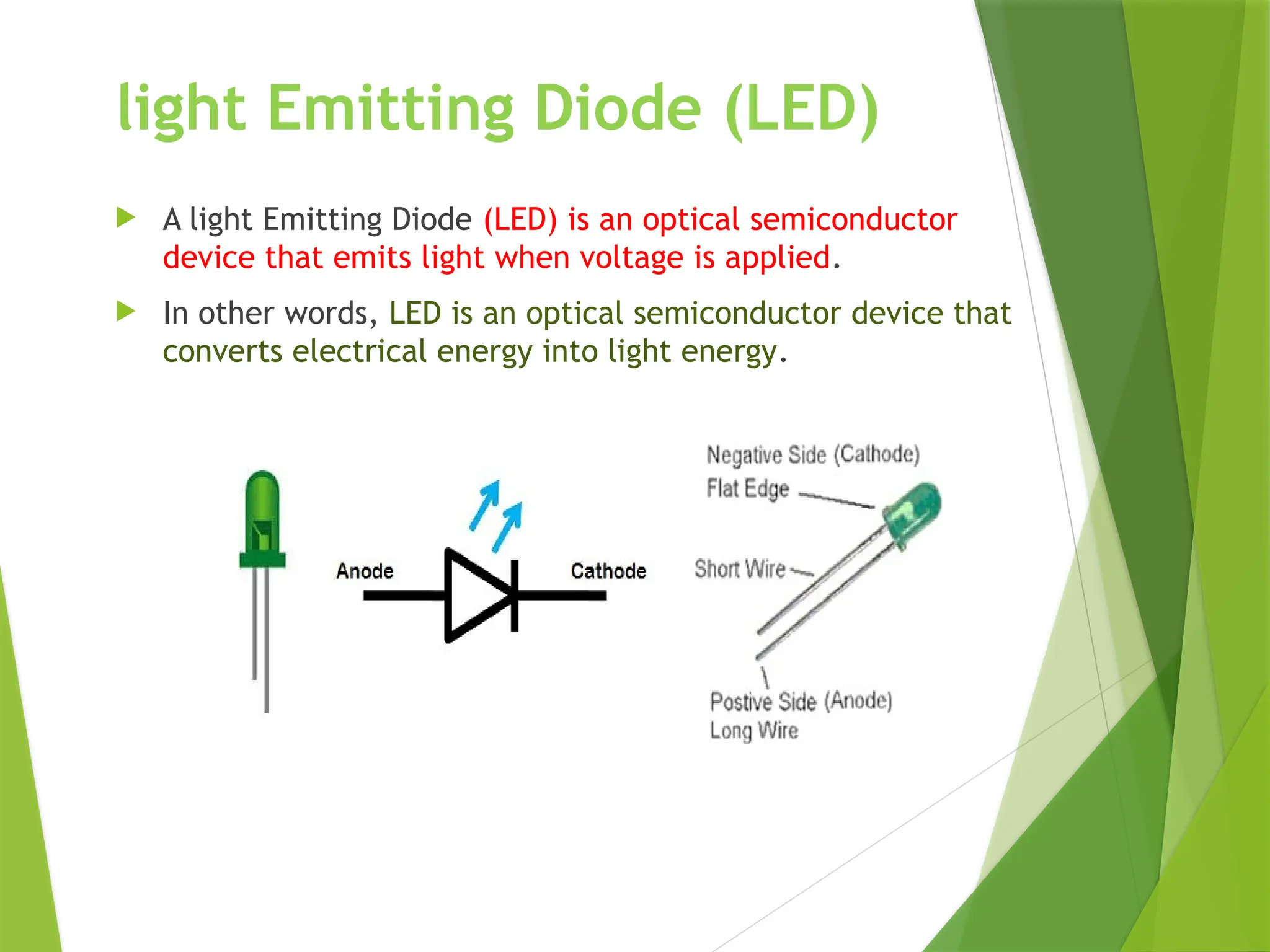
light Emitting Diode(LED)
A light Emitting Diode (LED) is an optical semiconductor
device that emits light when voltage is applied.
In other words, LED is an optical semiconductor device that
converts electrical energy into light energy.
14.
LED Construction
Thethree semiconductor layers deposited on the
substrate are n-type semiconductor, p-type
semiconductor and active region.
Active region is present in between the n-type and p-
type semiconductor layers
15.
When LEDis forward biased, free electrons from n-type
semiconductor and holes from p-type semiconductor are
pushed towards the active region.
When free electrons from n-side and holes from p-side
recombine with the opposite charge carriers (free
electrons with holes or holes with free electrons) in
active region, an invisible or visible light is emitted.
In LED, most of the charge carriers recombine at active
region. Therefore, most of the light is emitted by the active
region. The active region is also called as depletion
region.
16.
Working of LED
Light Emitting Diode (LED) works only in forward bias condition.
When Light Emitting Diode (LED) is forward biased, the free
electrons from n-side and the holes from p-side are pushed
towards the junction.
When free electrons reach the junction or depletion region, some
of the free electrons recombine with the holes in the positive
ions. We know that positive ions have less number of electrons
than protons. Therefore, they are ready to accept electrons.
Thus, free electrons recombine with holes in the depletion
region.
In the similar way, holes from p-side recombine with electrons in
the depletion region.
17.
The freeelectrons from n-type semiconductor cross the p-n
junction and recombines with holes in p-type
semiconductor. In the similar way, holes from p-type
semiconductor cross the p-n junction and recombines with
free electrons in the n-type semiconductor.
Thus, recombination takes place in depletion region as well
as in p-type and n-type semiconductor.
The free electrons in the conduction band releases energy
in the form of light before they recombine with holes in
the valence band.
18.
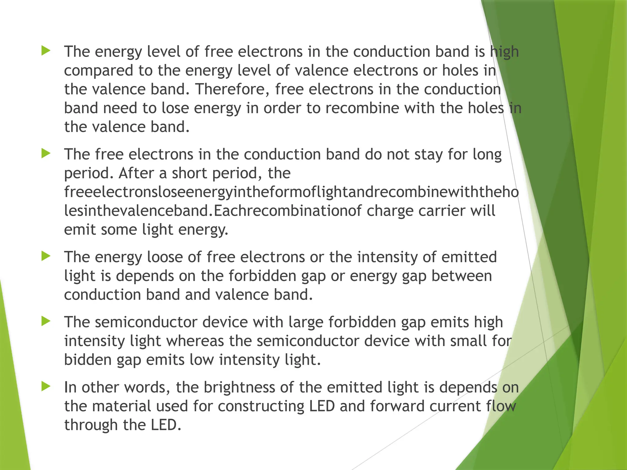
The energylevel of free electrons in the conduction band is high
compared to the energy level of valence electrons or holes in
the valence band. Therefore, free electrons in the conduction
band need to lose energy in order to recombine with the holes in
the valence band.
The free electrons in the conduction band do not stay for long
period. After a short period, the
freeelectronsloseenergyintheformoflightandrecombinewiththeho
lesinthevalenceband.Eachrecombinationof charge carrier will
emit some light energy.
The energy loose of free electrons or the intensity of emitted
light is depends on the forbidden gap or energy gap between
conduction band and valence band.
The semiconductor device with large forbidden gap emits high
intensity light whereas the semiconductor device with small for
bidden gap emits low intensity light.
In other words, the brightness of the emitted light is depends on
the material used for constructing LED and forward current flow
through the LED.
19.
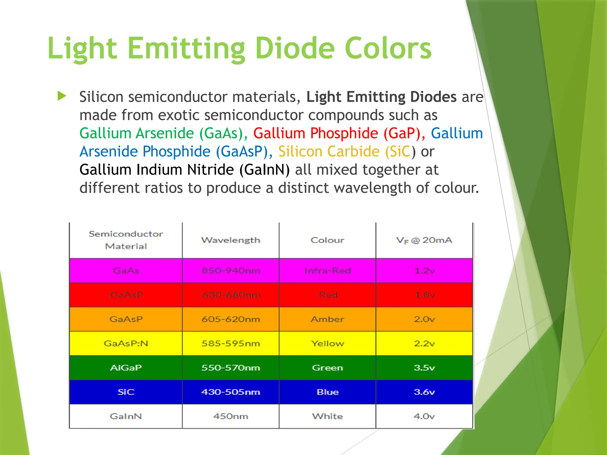
Light Emitting DiodeColors
Silicon semiconductor materials, Light Emitting Diodes are
made from exotic semiconductor compounds such as
Gallium Arsenide (GaAs), Gallium Phosphide (GaP), Gallium
Arsenide Phosphide (GaAsP), Silicon Carbide (SiC) or
Gallium Indium Nitride (GaInN) all mixed together at
different ratios to produce a distinct wavelength of colour.
20.
Light Emitting DiodesI-V
Characteristics
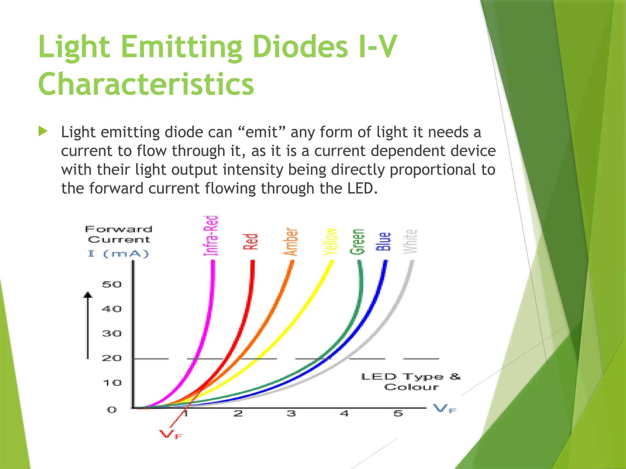
Light emitting diode can “emit” any form of light it needs a
current to flow through it, as it is a current dependent device
with their light output intensity being directly proportional to
the forward current flowing through the LED.
21.
Advantages of LED
The brightness of light emitted by LED is depends on the
current flowing through the LED. Hence, the brightness of LED
can be easily controlled by varying the current. This makes
possible to operate LED displays under different ambient
lighting conditions.
Light emitting diodes consume low energy.
LEDs are very cheap and readily available.
LEDs are light in weight.
Smaller size.
LEDs have longer lifetime.
LEDs operates very fast. They can be turned on and off in very
less time.
LEDs do not contain toxic material like mercury which is used in
fluorescent lamps.
LEDs can emit different colors of light.
22.
Disadvantages of LED
LEDs need more power to operate than normal p-n
junction diodes.
Luminous efficiency of LEDs is low.
23.
Applications of LED
Calculators
Picture phones
Traffic signals
Digital computers
Multi-meters
Digital watches
Camera flashes
Aviation lighting
24.
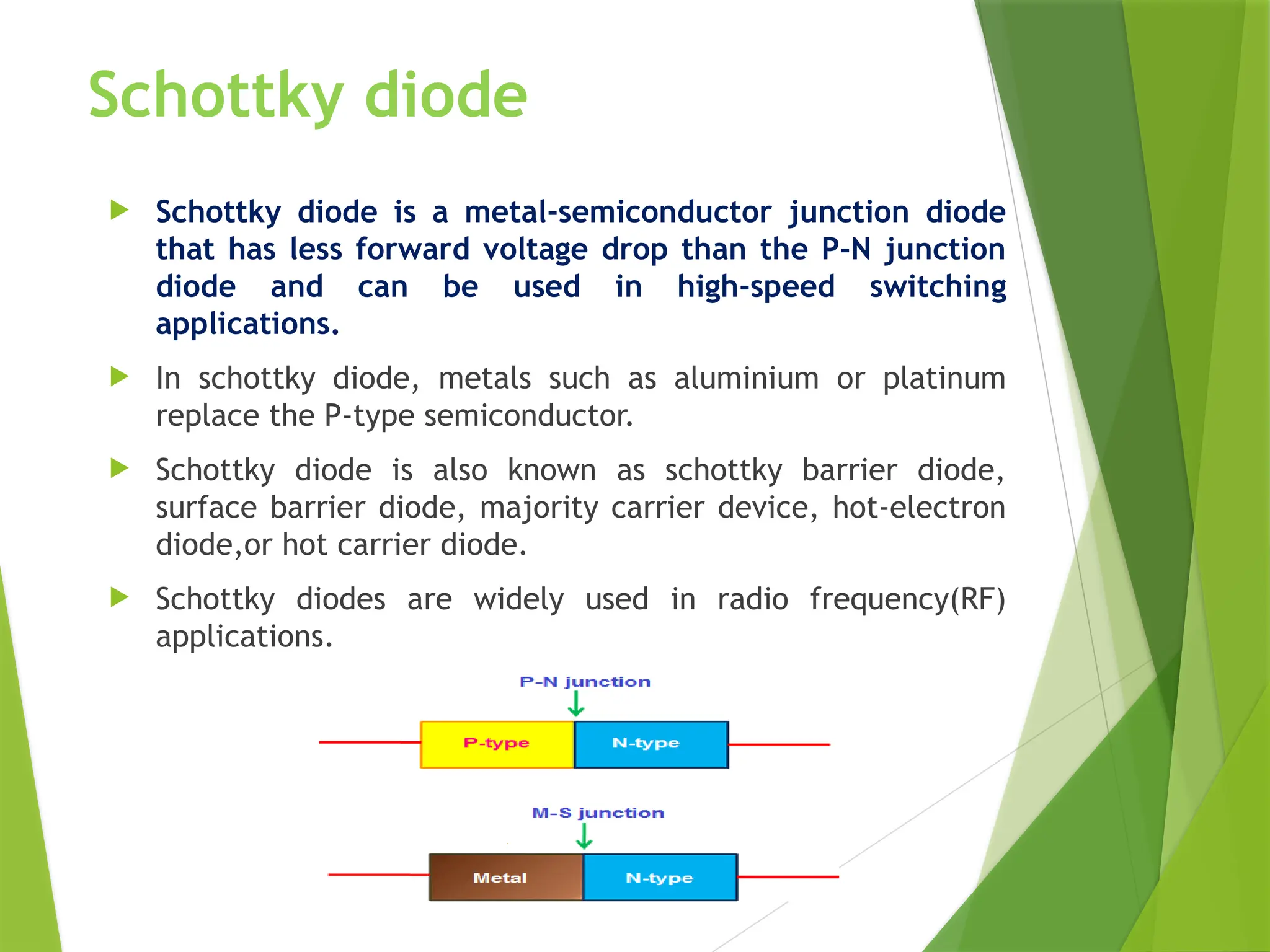
Schottky diode
Schottkydiode is a metal-semiconductor junction diode
that has less forward voltage drop than the P-N junction
diode and can be used in high-speed switching
applications.
In schottky diode, metals such as aluminium or platinum
replace the P-type semiconductor.
Schottky diode is also known as schottky barrier diode,
surface barrier diode, majority carrier device, hot-electron
diode,or hot carrier diode.
Schottky diodes are widely used in radio frequency(RF)
applications.
25.
When aluminiumor platinum metal is joined with N-type
semiconductor, a junction is formed between the metal
and N-type semiconductor. This junction is known as a
metal-semiconductor junction or M-S junction.
A metal-semiconductor junction formed between a metal
and n-type semiconductor creates a barrier or depletion
layer known as a schottky barrier.
26.
Schottky diodecan switch on and off much faster than the p-n
junction diode. Also, the schottky diode produces less
unwanted noise than p-n junction diode. These two
characteristics of the schottky diode make it very useful in
high-speed switching power circuits.
A silicon diode has a voltage drop of 0.6 to 0.7 volts, while a
schottky diode has a voltage drop of 0.2 to 0.3 volts. Voltage
loss or voltage drop is the amount of voltage wasted to turn on
a diode.
In silicon diode,0.6to 0.7 volts is wasted to turn on the diode,
whereas in schottky diode, 0.2 to 0.3 volts is wasted to turn on
the diode. Therefore, the schottky diode consumes less
voltage to turn on.
27.
Appearance and Symbolof
schottky diode
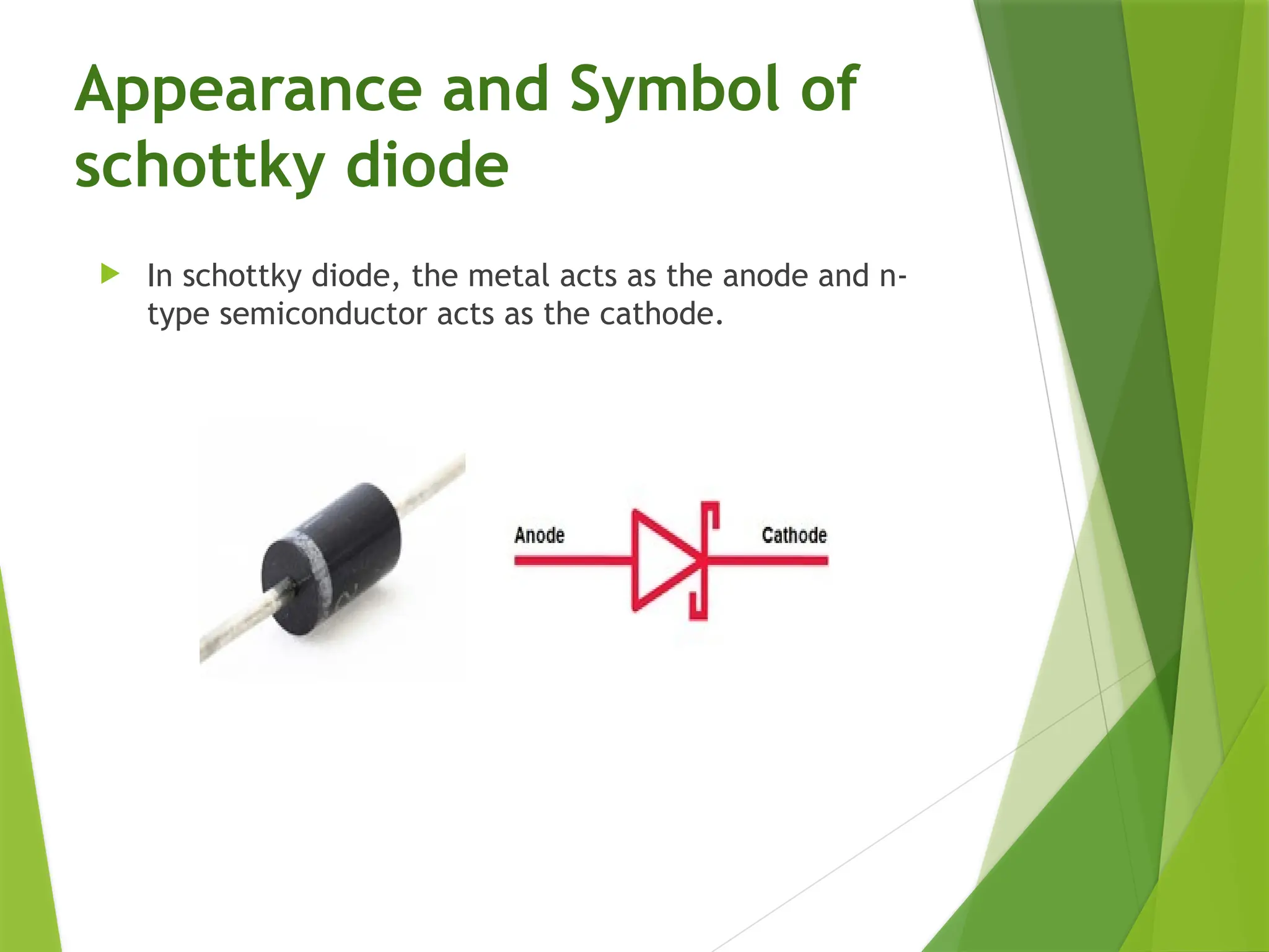
In schottky diode, the metal acts as the anode and n-
type semiconductor acts as the cathode.
28.
Forward Biased SchottkyDiode
If the positive terminal of the battery is connected to the
metal and the negative terminal of the battery is connected to
the n-type semiconductor, the schottky diode is said to be
forward biased.
When a forward bias voltage is applied to the schottky diode, a
large number of free electrons are generated in the n-type
semiconductor and metal. However, the free electrons in n-
type semiconductor and metal cannot cross the junction unless
the applied voltage is greater than 0.2volts.
If the applied voltage is greater than 0.2 volts, the free
electrons gain enough energy and overcomes the built-in-
voltage of the depletion region. As a result, electric current
starts flowing through the schottky diode.
If the applied voltage is continuously increased, the depletion
region becomes very thin and finally disappears.
29.
Reverse bias schottkydiode
If the negative terminal of the battery is connected to the metal
and the positive terminal of the battery is connected to the n-type
semiconductor, the schottky diode is said to be reverse biased.
When a reverse bias voltage is applied to the schottky diode, the
depletion width increases. As a result, the electric current stops
flowing. However,a small leakage current flows due to the
thermally excited electrons in the metal.
If the reverse bias voltage is continuously increased, the electric
current gradually increases due to the weak barrier. If the reverse
bias voltage is largely increased, a sudden rise in electric current
takes place. This sudden rise in electric current causes depletion
region to break down which may permanently damage the device.
30.
V-I characteristics ofschottky
diode
The V-I (Voltage-Current) characteristics of schottky diode is
shown in the below figure. The vertical line in the below figure
represents the current flow in the schottky diode and the
horizontal line represents the voltage applied across the schottky
diode.
The V-I characteristics of schottky diode is almost similar to the P-
N junction diode. However, the forward voltage drop of schottky
diode is very low as compared to the P-N junction diode.
31.
The forwardvoltage drop of schottky diode is 0.2 to 0.3
volts whereas the forward voltage drop of silicon P-N
junction diode is 0.6 to 0.7 volts.
If the forward bias voltage is greater than 0.2 or 0.3 volts,
electric current starts flowing through the schottky diode.
In schottky diode, there verse saturation current occurs at
a very low voltage as compared to the silicon diode.
32.
Applications Of SchottkyDiodes
Schottky diodes are used as general-purpose rectifiers.
Schottky diodes are used in radio frequency(RF)
applications.
Schottky diodes are widely used in power supplies.
Schottky diodes are used to detect signals.
Schottky diodes are used in logic circuits.
33.
Varactor Diode
Varactordiode is a P-N junction diode whose capacitance is varied
by varying the reverse voltage.
The term varactor is originated from a variable capacitor.
Varactor diode operates only in reverse bias.
The varactor diode acts like a variable capacitor under reverse bias.
Varactor diode is also sometimes referred to as varicap diode,
tuning diode, variable reactance diode or variable capacitance
diode.
The circuit symbol of the varactor diode is almost similar to the
normal p-n junction diode. Two parallel lines at the cathode side
represents two conductive plates and the space between these two
parallel lines represents dielectric.
34.
A capacitoris an electronic component that stores electrical
energy or electric charge in the form of an electric field.
The basic capacitor is made up of two parallel conductive
plates separated by a dielectric. The two conductive plate’s
acts like electrodes and the dielectric acts like an insulator.
35.
The conductiveplates are good conductors of electricity so
they easily allow electric current through them.
On the other hand, a dielectric is poor conductor of
electricity so it does not allow electric current through it
but it allows electric field or electric force.
When voltage is applied to the capacitor in such a way that
the negative terminal of the battery is connected to the
right side electrode or plate and the positive terminal of
the battery is connected to the left side electrode, the
capacitor starts storing electric charge.
36.
Construction
The varactordiode is made up of the p-type and n-type
semiconductor.
In the n-type semiconductor, free electrons are the majority
carriers and holes are the minority carriers. So the free
electrons carry most of the electric current in n-type
semiconductor.
In the p-type semiconductor, holes are the majority carriers
and free electrons are the minority carriers. So the holes carry
most of the electric current in p-type semiconductor.
37.
When ap-type semiconductor is in contact with the n-type
semiconductor, a p-n junction is formed between them.
This p-n junction separates the p-type and n-type
semiconductor.
At the p-n junction, a depletion region is created. A
depletion region is a region where mobile charge
carriers(free electrons and holes) are absent.
The depletion region is made up of positive and negative
ions (charged atoms). These positive and negative ions
does not move from one place to another place.
The depletion region blocks free electrons from n-side and
holes from p-side. Thus, depletion region blocks electric
current across the p-n junction.
38.
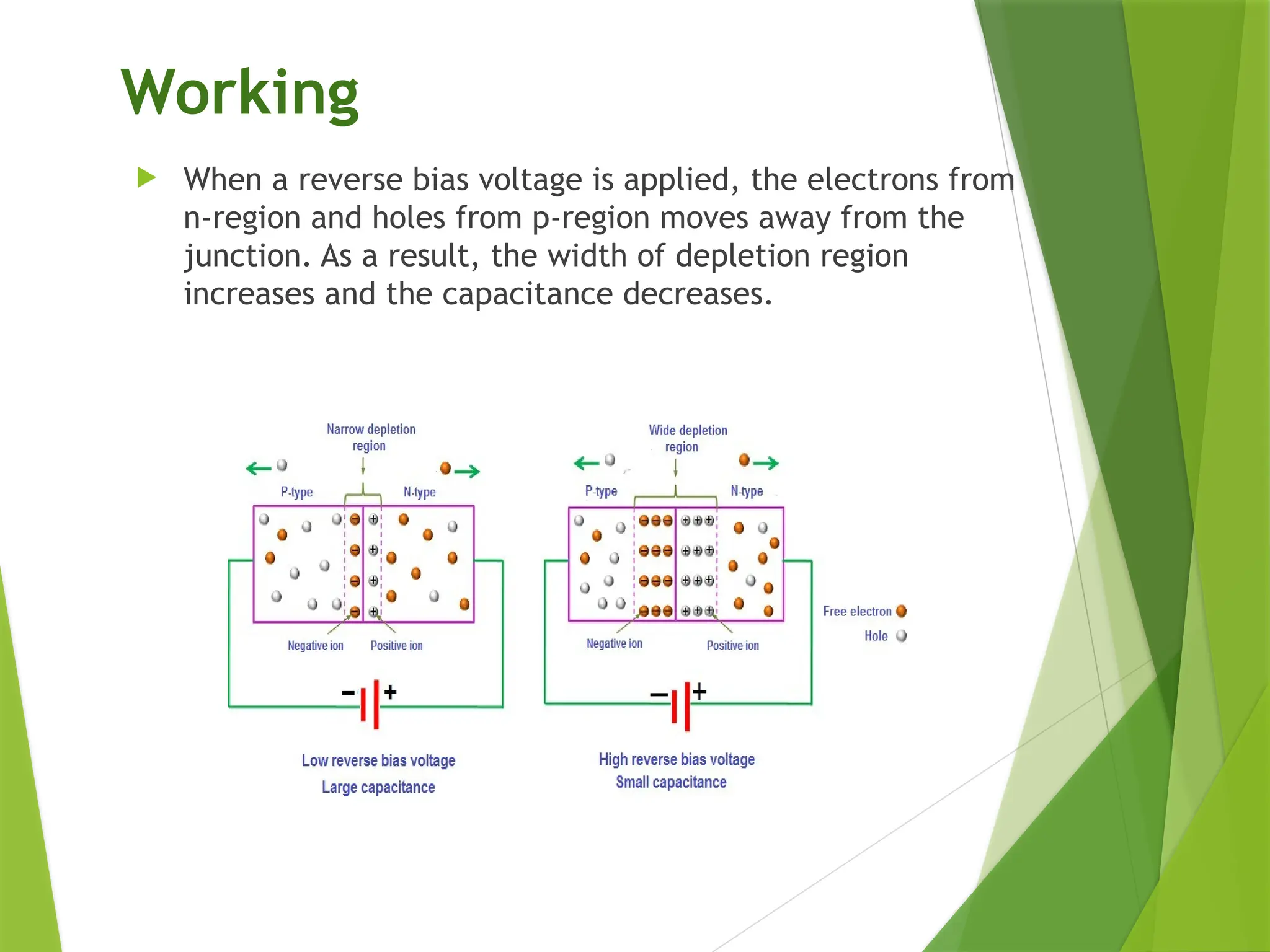
Working
When areverse bias voltage is applied, the electrons from
n-region and holes from p-region moves away from the
junction. As a result, the width of depletion region
increases and the capacitance decreases.
39.
However, ifthe applied reverse bias voltage is very low the
capacitance will be very large.
The capacitance is inversely proportional to the width of
the depletion region and directly proportional to the
surface area of the p-region and n-region. So the
capacitance decreases as the as the width of depletion
region increases.
If the reverse bias voltage is increased, the width of
depletion region further increases and the capacitance
further decreases.
On the other hand, if the reverse bias voltage is reduced,
the width of depletion region decreases and the
capacitance increases.
40.
Thus, anincrease in reverse bias voltage increases the width of
the depletion region and decreases the capacitance of a varactor
diode.
The decrease in capacitance means the decrease in storage
charge. So the reverse bias voltage should be kept at a minimum
to achieve larges to rage charge. Thus, capacitance or transition
capacitance can be varied by varying the voltage.
In a fixed capacitor, the capacitance will not be varied whereas,
in variable capacitor, the capacitance is varied.
In a varactor diode, the capacitance is varied when the voltage
is varied. So the varactor diode is a variable capacitor. The
capacitance of a varactor diode is measured in pico farads(pF).
41.
Applications of varactordiode
Varactor diode is used in frequency multipliers.
Varactor diode is used in parametric amplifiers.
Varactor diode is used in voltage-controlled oscillators.
What do you mean by oscillator?
An oscillator is a circuit or device that generates a periodic, oscillating
signal, typically alternating current (AC), without needing any external
input signal. In simpler terms, it's a component that converts direct
current (DC) power into a repeating AC signal of a specific frequency.
What do you mean by amplifier?
An amplifier is an electronic device that boosts the strength of a signal,
usually by increasing its voltage, current, or power.
What do you mean by multiplier?
In simple terms, a multiplier is something that increases or amplifies the
effect of something else. It can be a number used in multiplication, a
device that enhances an effect, or a concept in economics describing
how an initial change in spending can lead to a larger overall change in
economic activity.
42.
Tunnel diode
ATunnel diode is a heavily doped p-n junction diode in
which the electric current decreases as the voltage
increases.
In tunnel diode, electric current is caused by
“Tunneling”. The tunnel diode is used as a very fast
switching device in computers.
It is also used in high-frequency oscillators and amplifiers.
43.
Appearance and Symbolof
tunnel diode
The circuit symbol of tunnel diode is shown in the below
figure.
In tunnel diode, the p-type semiconductor act as an
anode and then-type semiconductor act as a cathode.
44.
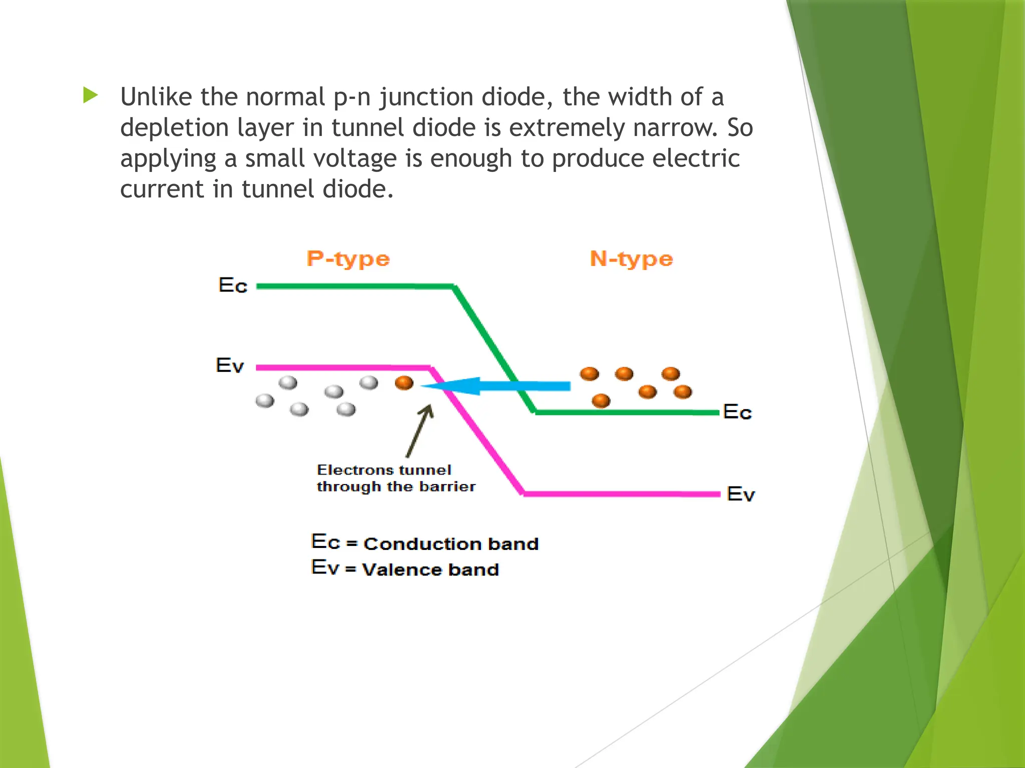
The operationof tunnel diode depends on the quantum
mechanics principle known as “Tunneling”.
In electronics, tunneling means a direct flow of
electrons across the small depletion region from n-side
conduction band into the p-side valence band.
Quantum mechanics says that the electrons will directly
penetrate through the depletion layer or barrier if the
depletion width is very small.
45.
The germaniummaterial is commonly used to make the
tunnel diodes. They are also made from other types of
materials such as gallium arsenide, gallium anti monide,
and silicon.
46.
In tunneldiode, the p-type and n-type semiconductor is
heavily doped which means a large number of impurities
are introduced into the p-type and n-type semiconductor.
This heavy doping process produces an extremely narrow
depletion region. The concentration of impurities in tunnel
diode is 1000 times greater than the normal p-n junction
diode.
In normal p-n junction diode, the depletion width is large
as compared to the tunnel diode. This wide depletion layer
or depletion region in normal diode opposes the flow of
current. Hence, depletion layer acts as a barrier.
To overcome this barrier, we need to apply sufficient
voltage. When sufficient voltage is applied, electric
current starts flowing through the normal p-n junction
diode.
47.
Unlike thenormal p-n junction diode, the width of a
depletion layer in tunnel diode is extremely narrow. So
applying a small voltage is enough to produce electric
current in tunnel diode.
48.
The depletionlayer of tunnel diode is very small. It is in
nano meters. So the electrons can directly tunnel across
the small depletion region from n-side conduction band in
to the p-side valence band.
In ordinary diodes, current is produced when the applied
voltage is greater than the built-in voltage of the
depletion region. But in tunnel diodes, a small voltage
which is less than the built-in voltage of depletion region
is enough to produce electric current.
In tunnel diodes, the electrons need not overcome the
opposing force from the depletion layer to produce
electric current. The electrons can directly tunnel from
the conduction band of n-region into the valence band of
p-region. Thus, electric current is produced in tunnel
diode.
49.
Step1: Unbiased tunneldiode
When no voltage is applied to the tunnel diode, it is said
to be an unbiased tunnel diode. In tunnel diode, the
conduction band of the n-type material overlaps with
the valence band of the p-type material because of the
heavy doping.
50.
Because ofthis overlapping, the conduction band
electrons at n-side and valence band holes at p-side are
nearly at the same energy level. So when the
temperature increases, some electrons tunnel from the
conduction band of n-region to the valence band of p-
region. In a similar way, holes tunnel from the valence
band of p-region to the conduction band of n-region.
However, the net current flow will be zero because an
equal number of charge carriers (free electrons and holes)
flow in opposite directions.
51.
Step2: Small voltageapplied to the tunnel diode
When a small voltage is applied to the tunnel diode which is less
than the built-in voltage of the depletion layer, no forward
current flows through the junction.
However, a small number of electrons in the conduction band of
the n-region will tunnel to the empty states of the valence band
in p-region. This will create a small forward bias tunnel current.
Thus, tunnel current starts flowing with a small application of
voltage.
52.
Step3: Applied voltageis
slightly increased
When the voltage applied to the tunnel diode is
slightly increased, a large number of free electrons
at n-side and holes at p-side are generated. Because
of the increase in voltage, the overlapping of the
conductionbandandvalencebandisincreased.Insimple
words,theenergylevelofann-
sideconductionbandbecomes exactly equal to the
energy level of a p-side valence band. As a result,
maximum tunnel current lows.
53.
Step4: Applied voltageis
further increased
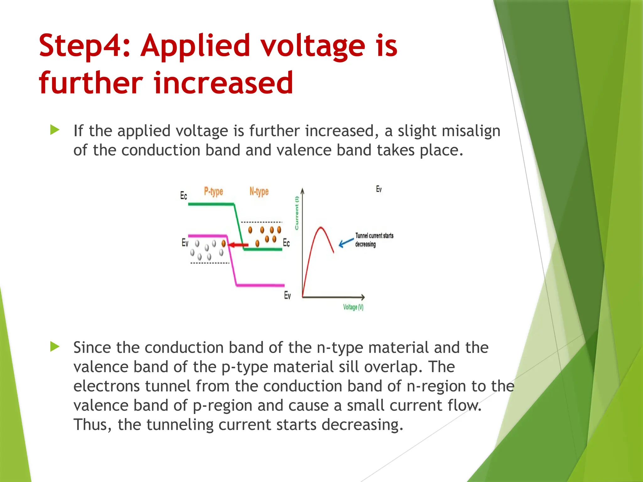
If the applied voltage is further increased, a slight misalign
of the conduction band and valence band takes place.
Since the conduction band of the n-type material and the
valence band of the p-type material sill overlap. The
electrons tunnel from the conduction band of n-region to the
valence band of p-region and cause a small current flow.
Thus, the tunneling current starts decreasing.
54.
Step 5: Appliedvoltage is largely
increased
If the applied voltage is largely increased, the tunneling
current drops to zero. At this point, the conduction band and
valence band no longer overlap and the tunnel diode operates
in the same manner as a normal p-n junction diode.
55.
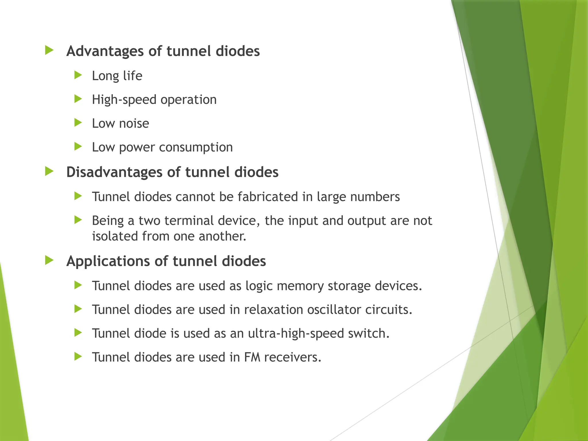
Advantages oftunnel diodes
Long life
High-speed operation
Low noise
Low power consumption
Disadvantages of tunnel diodes
Tunnel diodes cannot be fabricated in large numbers
Being a two terminal device, the input and output are not
isolated from one another.
Applications of tunnel diodes
Tunnel diodes are used as logic memory storage devices.
Tunnel diodes are used in relaxation oscillator circuits.
Tunnel diode is used as an ultra-high-speed switch.
Tunnel diodes are used in FM receivers.
56.
Photo diode
Aphoto diode is a p-n junction or pin semiconductor device
that consumes light energy to generate electric current.
Photo diodes are specially designed to operate in reverse
bias condition.
Photo diode is very sensitive to light so when light or
photons falls on the photo diode it easily convert slight into
electric current.
Solar cell is also known as large area photodiode because it
converts solar energy or light energy into electric energy.
However, solar cell works only at bright light.
57.
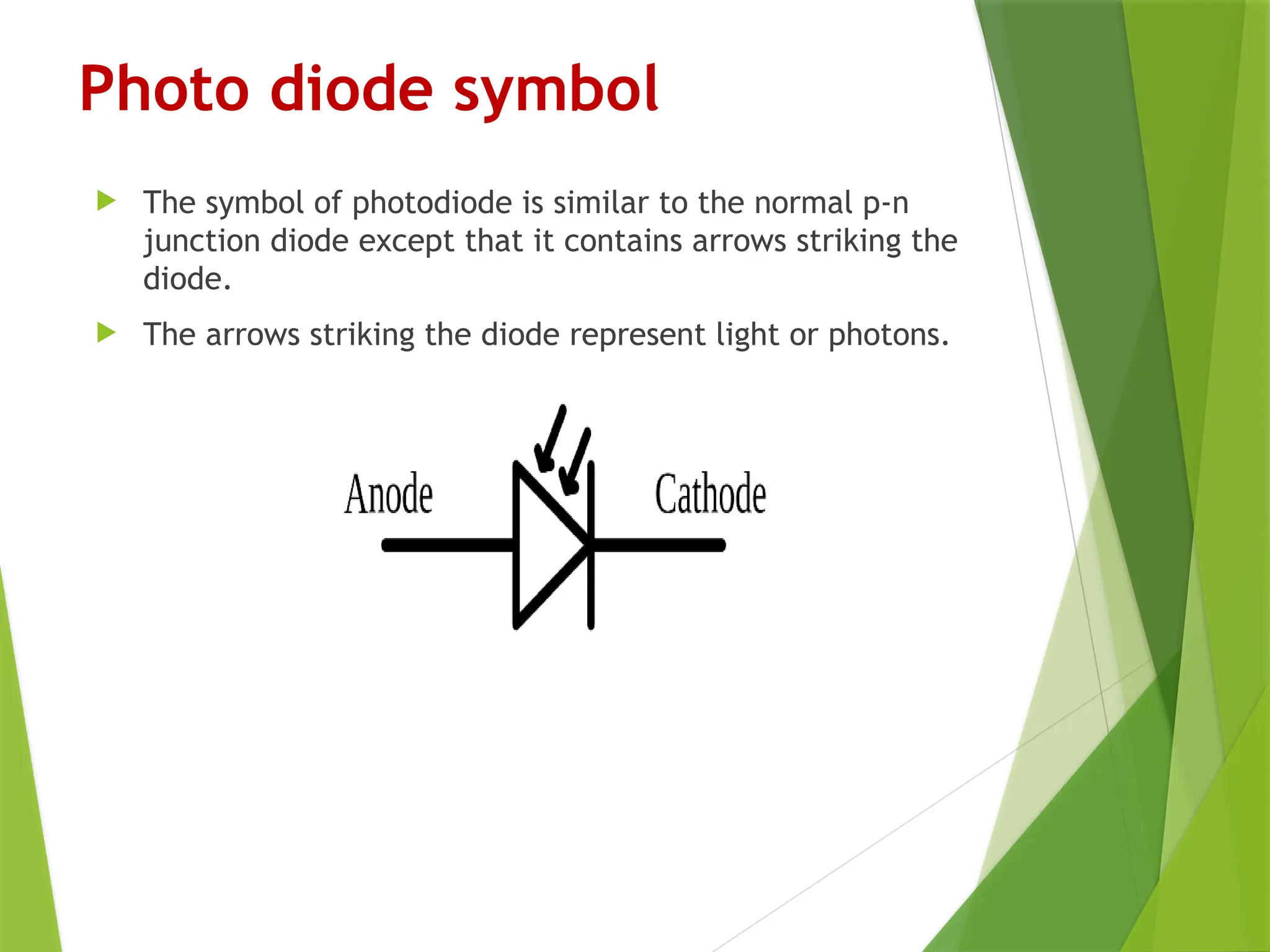
Photo diode symbol
The symbol of photodiode is similar to the normal p-n
junction diode except that it contains arrows striking the
diode.
The arrows striking the diode represent light or photons.
58.
Principle of Photodiode
It works on the principle of Photo electric effect.
The operating principle of the photodiode is such that
when the junction of this two terminal semiconductor
device is illuminated then electric current starts flowing
through it. Only minority current flows through the device
when the certain reverse potential is applied to it.
59.
Construction of Photodiode
The PN junction of the device placed inside a glass
material. This is done to order to allow the light energy
to pass through it. As only the junction is exposed to
radiation, thus, the other portion of the glass material is
painted black or is metallized.
60.
Operational Modes ofPhoto
diode
Photovoltaic mode: It is also known as zero bias mode
because no any external reverse potential is provided to
the device. However, the flow of minority carrier will take
place when the device is exposed to light.
Photoconductive mode: When a certain reverse potential
is applied to the device then it behaves as a photo
conductive device. Here, an increase in depletion width is
seen with the corresponding change in reverse voltage.
61.
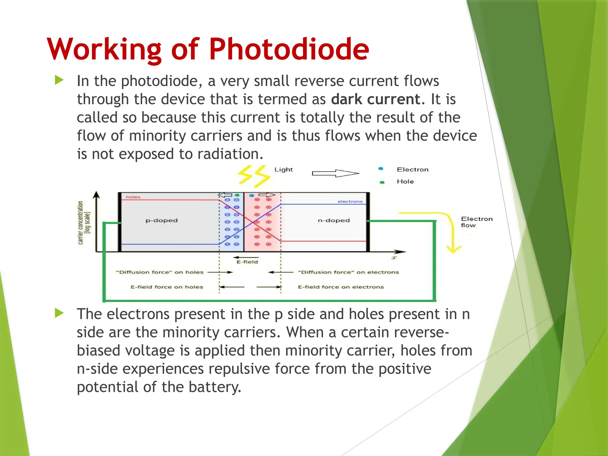
Working of Photodiode
In the photodiode, a very small reverse current flows
through the device that is termed as dark current. It is
called so because this current is totally the result of the
flow of minority carriers and is thus flows when the device
is not exposed to radiation.
The electrons present in the p side and holes present in n
side are the minority carriers. When a certain reverse-
biased voltage is applied then minority carrier, holes from
n-side experiences repulsive force from the positive
potential of the battery.
62.
Similarly, theelectrons present in the p side experiences
repulsion from the negative potential of the battery. Due
to this movement electron and hole recombine at the
junction resultantly generating depletion region at the
junction. Due to this movement, a very small reverse
current flows through the device known as dark current.
63.
The combinationof electron and hole at the junction generates
neutral atom at the depletion. Due to which any further flow of
current is restricted. Now, the junction of the device is
illuminated with light.
As the light falls on the surface of the junction, then the
temperature of the junction gets increased. This causes the
electron and hole to get separated from each other.
At the two gets separated then electrons from n side gets
attracted towards the positive potential of the battery.
Similarly, holes present in the p side get attracted to the negative
potential of the battery. This movement then generates a high
reverse current through the device. With the rise in the light
intensity, more charge carriers are generated and flow through
the device. Thereby, producing a large electric current through
the device.
This current is then used to drive other circuits of the system. So,
we can say the intensity of light energy is directly proportional to
the current through the device. Only positive biased potential can
put the device in no current condition in case of the photo diode.
64.
Characteristics of Photodiode
The vertical line represents there verse current flowing through the
device and the horizontal line represents the reverse biased potential.
The above curve represents the dark current that generates due to
minority carriers in the absence of light. As we can see in the above figure
that all the curve shows almost equal spacing in between them. This is so
because current proportionally increases with the luminous flux.
65.
Advantages
Itshows a quick response when exposed to light.
Photodiode offers high operational speed.
It provides a linear response.
It is a low-cost device.
Disadvantages
It is a temperature dependent device. And shows poor
temperature stability.
When low illumination is provided, then amplification
is necessary.
66.
Applications
Photo diodes majorlyfind its use in counters and switching
circuits.
Photo diodes are extensively used in an optical
communication system.
Logic circuits and encoders also make use of photo diode.
It is widely used in burglar alarm systems. In such alarm
systems, until exposure to radiation is not interrupted, the
current flows. As the light energy fails to fall on the device,
it sounds the alarm.