Downloaded 341 times


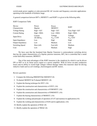
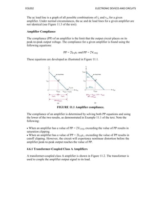
![EC6202 ELECTRONIC DEVICES AND CIRCUITS
8
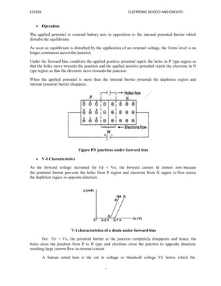
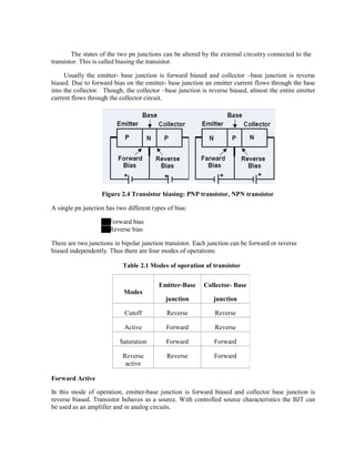
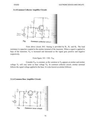
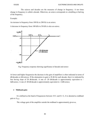
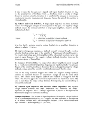
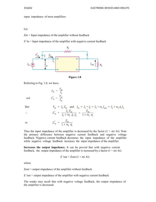
dc f
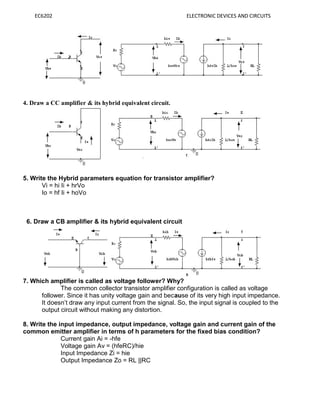
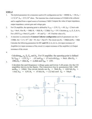
= I2
rms RF + I2
rms RL = {I2
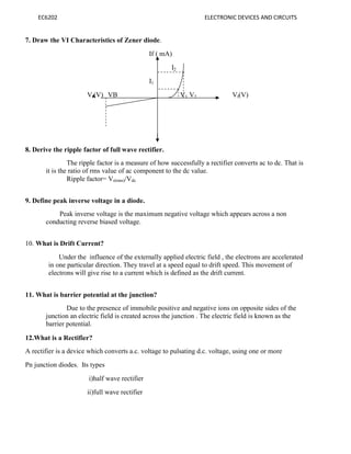
MAX/4}[RF + RL]
Rectification Efficiency, Ƞ = Pdc / Pac = {4/ 2
}[RL/ (RF + RL)] = 0.406/{1+ RF/RL }
If RF is neglected, the efficiency of half wave rectifier is 40.6%.
Ripple factor: It is defined as the amount of AC content in the output DC. It nothing but
amount of AC noise in the output DC. Less the ripple factor, performance of the rectifier is
more. The ripple factor of half wave rectifier is about 1.21 (full wave rectifier has about
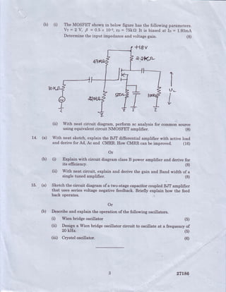
0.48). It can be calculated as follows:
The effective value of the load current I is given as sum of the rms values of
harmonic currents I1, I2, I3, I4 and DC current Idc.
I2
=I2
dc+I2
1+I2
2+I2
4 = I2
dc +I2
ac
Ripple factor, is given as γ = I ac / Idc = (I2
– I2
dc) / Idc = {( I rms / I 2
)-1} = K 2
– 1)
Where Kf is the form factor of the input voltage. Form factor is given as
Kf = Irms /Iavg = (Imax/2)/ (Imax/pi) = pi/2 = 1.57
So, ripple factor, γ = (1.572
– 1) = 1.21
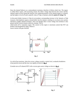
Peak Inverse Voltage: It is defined as the maximum voltage that a diode can with stand in
reverse bias. During the reverse bias as the diode do not conduct total voltage drops across the
diode. Thus peak inverse voltage is equal to the input voltage Vs.
Transformer Utilization Factor (TUF): The TUF is defined as the ratio of DC power is
delivered to the load and the AC rating of the transformer secondary. Half wave rectifier has
around 0.287 and full wave rectifier has around 0.693.
Half wave rectifier is mainly used in the low power circuits. It has very low performance when it is
compared with the other rectifiers.
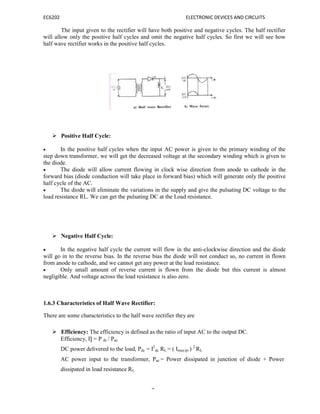
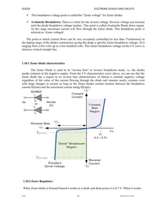
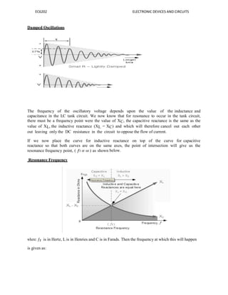
1.7 FULL WAVE RECTIFIER
Full wave rectifier rectifies the full cycle in the waveform i.e. it rectifies both the positive and
negative cycles in the waveform. We have already seen the characteristics and working of Half
Wave Rectifier. This Full wave rectifier has an advantage over the half wave i.e. it has average
output higher than that of half wave rectifier. The number of AC components in the output is less
than that of the input.
The full wave rectifier can be further divided mainly into following types.](https://image.slidesharecdn.com/ec6202edcnotes-170628094019/85/EC6202-ELECTRONIC-DEVICES-AND-CIRCUITS-NOTES-16-320.jpg)
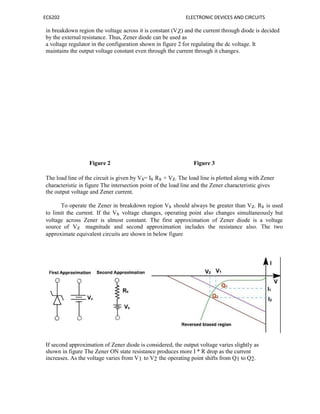
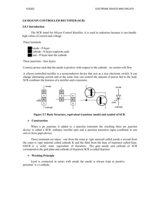
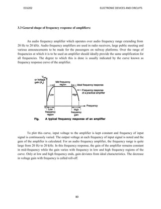
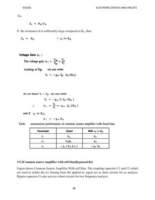
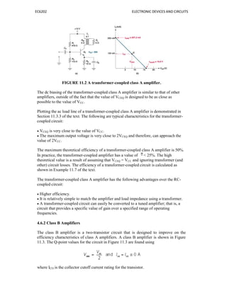
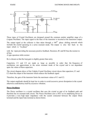
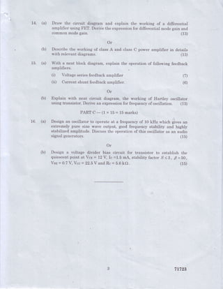
![EC6202 ELECTRONIC DEVICES AND CIRCUITS
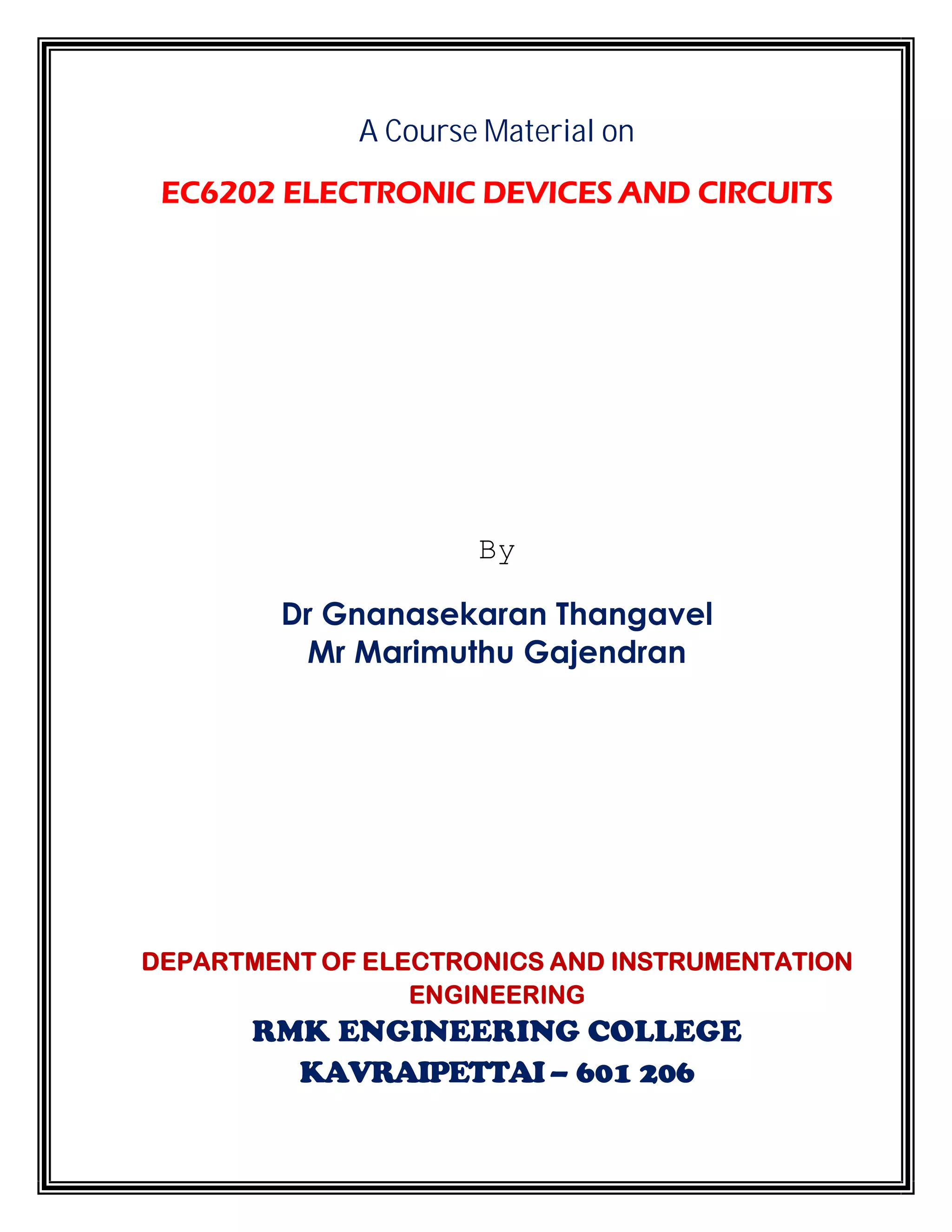
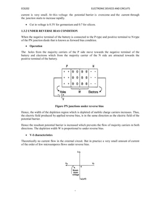
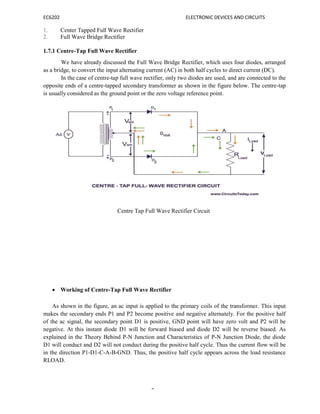
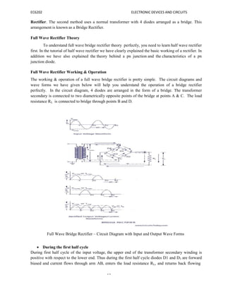
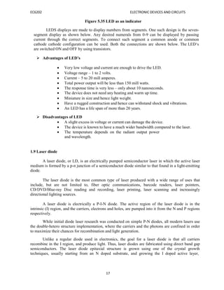
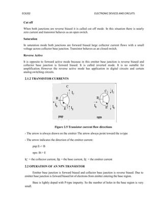
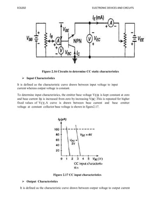
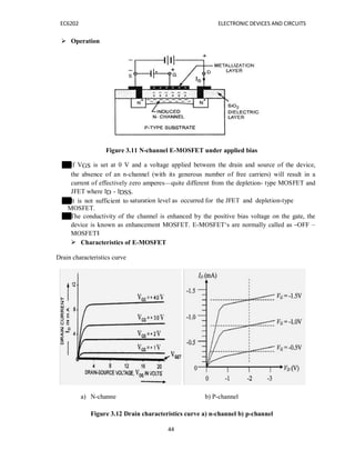
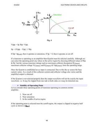
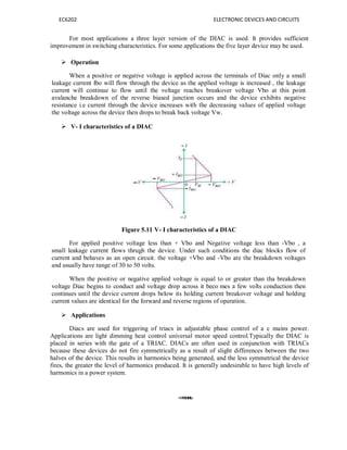
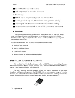
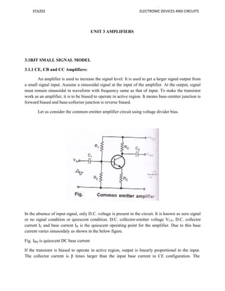
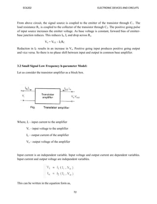
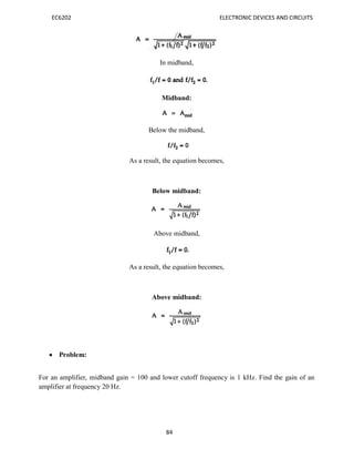
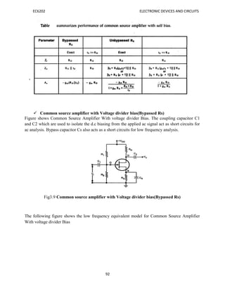
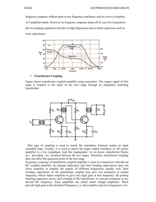
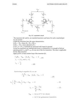
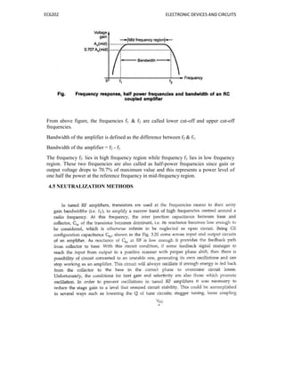
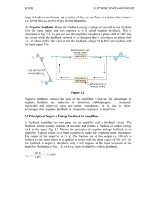
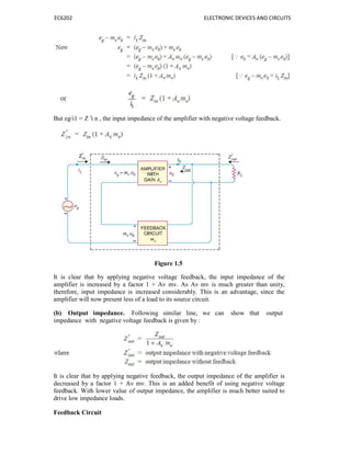
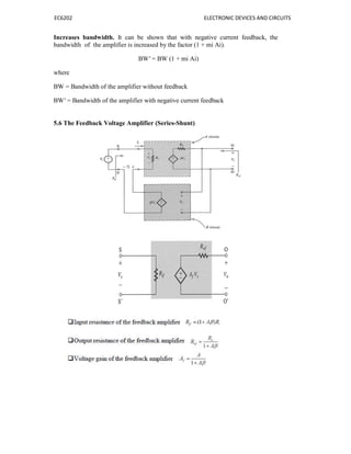
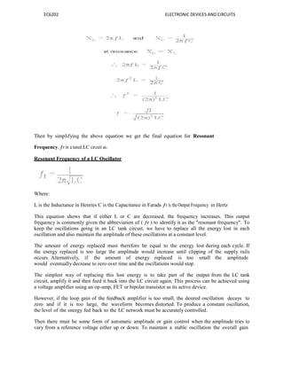
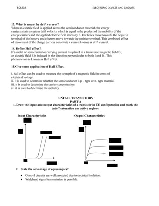
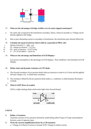
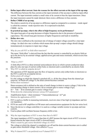
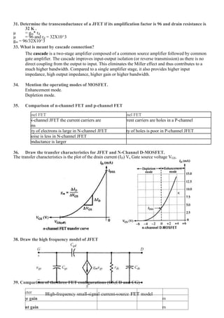
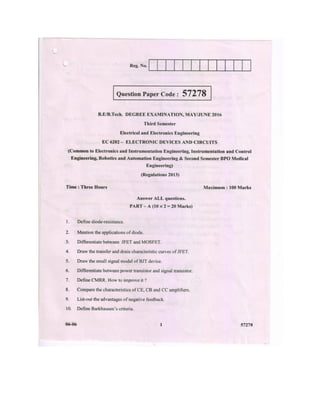
The symbolic representation of the two types of the BJT is shown in figure 2.2
Area:[C>E>B]
Figure 2.2 circuit symbol: NPN transistor ,PNP transistor
The area of collector layer is largest. So it can dissipate heat quickly.
Area of base layer is smallest and it is very thin layer.
Area of emitter layer is medium.
Doping level:[E>C>B]
Collector layer is moderately doped. So it has medium number of charges.
Base layer is lightly doped. So it has a very few number of charges.
Emitter layer is heavily doped. So it has largest number of charges.
Junctions:
There are two junctions in this transistor – junction J-1 and junction J-2.
The junction between
or C-B junction.
collector layer and base layer is called as collector-base junction
The junction between base layer and emitter layer is called as base-emitter junction
or B-E junction. The two junctions have almost same potential barrier voltage of 0.6V to
0.7V, just like in a diode.
Equivalent diode representation:
The transistor formed by back to back connection of two diodes
Figure 2.3 The equivalent diode representation for the NPN and PNP transistors](https://image.slidesharecdn.com/ec6202edcnotes-170628094019/85/EC6202-ELECTRONIC-DEVICES-AND-CIRCUITS-NOTES-32-320.jpg)
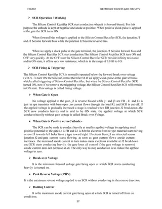
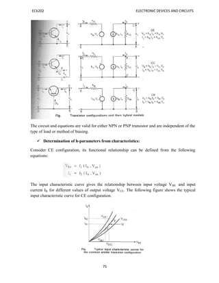
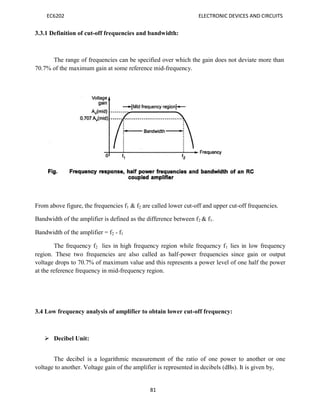
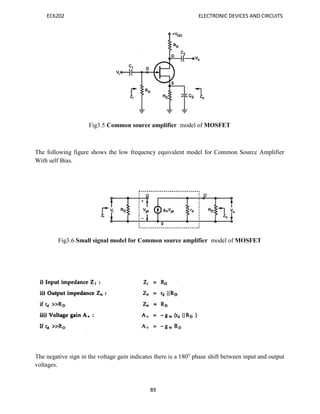
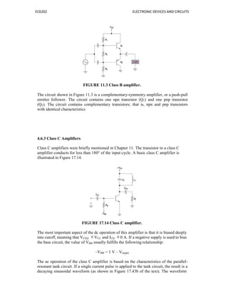
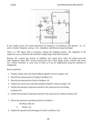
![EC6202 ELECTRONIC DEVICES AND CIRCUITS
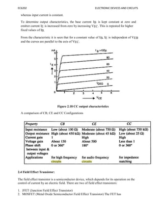
39
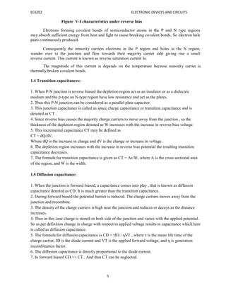
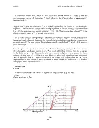
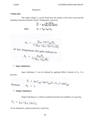
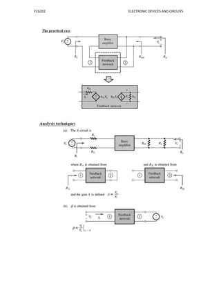
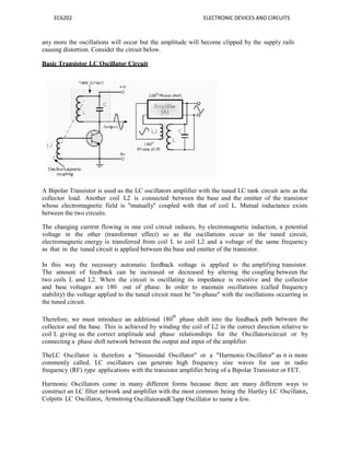
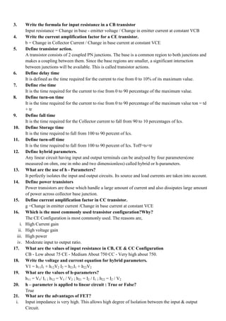
1
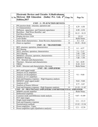
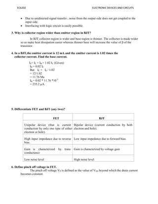
By reading the value of ID and VGS for a particular value of VDS, the transconductance curve
can be
plotted. The transconductance curve is a part of parabola. It has an equation of
Data sheet provides only IDSS and VGS(off) value. Using these values the transconductance curve
can be plotted.
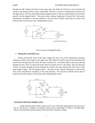
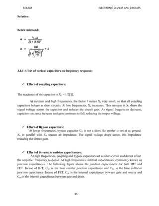
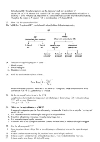
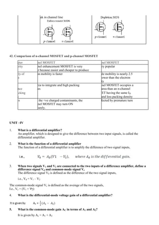
2.5 MOSFET (Metal Oxide Semiconductor Field Effect Transistor)
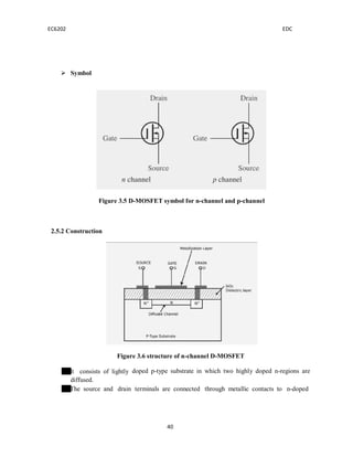
Like JFET, it has a source, Drain and Gate.
It is also called IGFET (Insulated Gate FET) because gate terminal is insulated from
channel. Therefore it has extremely high input resistance.
Types of MOSFET
It has two types
Depletion mode MOSFET
N-channel
P-channel
Enhancement mode MOSFET
N-channel
P-channel
The enhancement-type MOSFET is usually referred to as an E-MOSFET, and the depletion
type, a D-MOSFET. The drain current in a MOSFET is controlled by the gate-source voltage VGS.
2.5.1 Depletion mode-MOSFET [D-MOSFET]
In depletion mode of operation the bias voltage on the gate reduce the number of charge
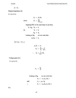
carriers in the channel and therefore reduce the drain current ID.It operates in both
depletion
mode and enhancement mode.](https://image.slidesharecdn.com/ec6202edcnotes-170628094019/85/EC6202-ELECTRONIC-DEVICES-AND-CIRCUITS-NOTES-47-320.jpg)
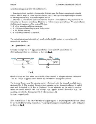
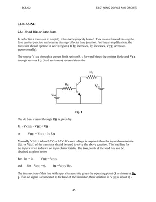
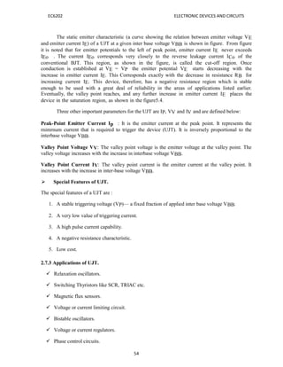
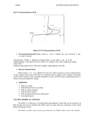
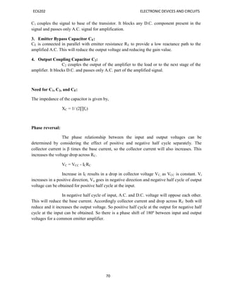
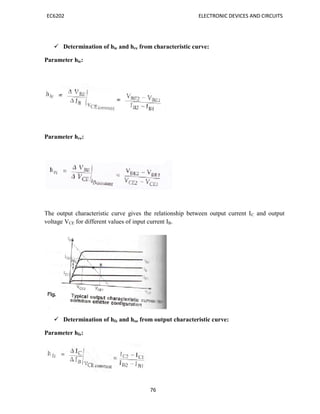
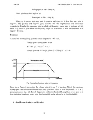
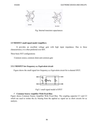
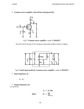
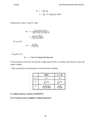
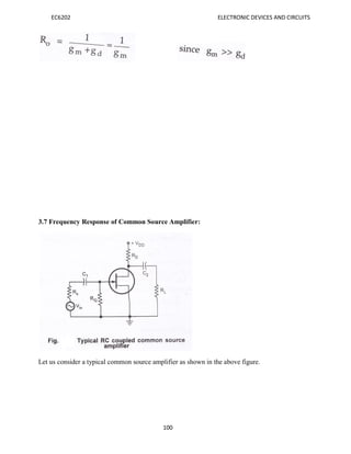
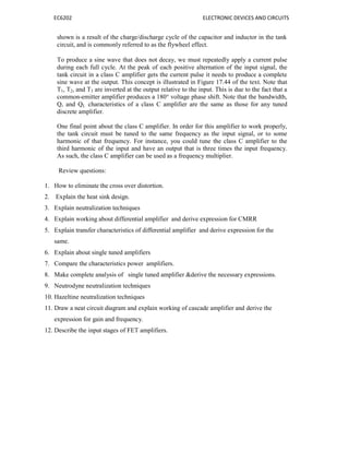
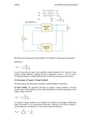
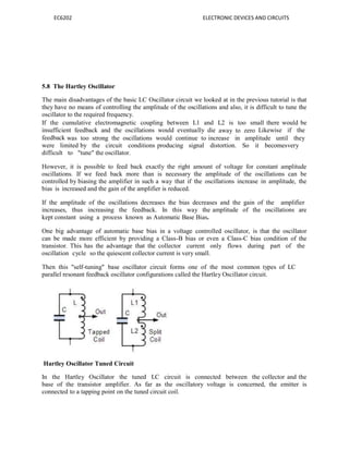
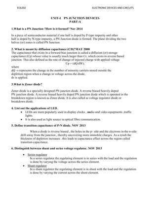
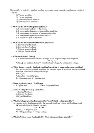
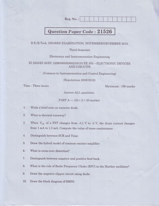
![42
EC6202 ELECTRONIC DEVICES AND CIRCUITS
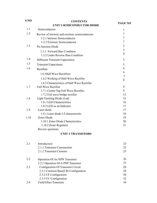
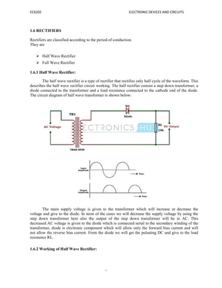
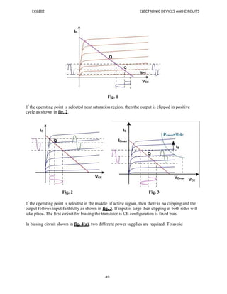
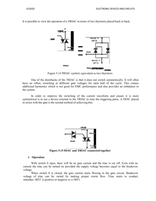
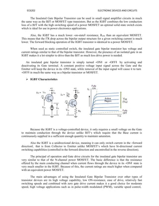
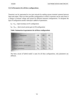
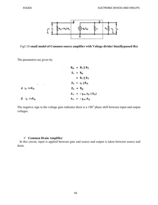
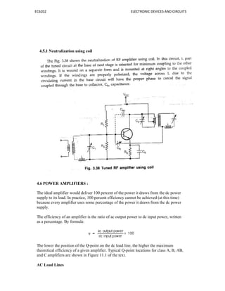
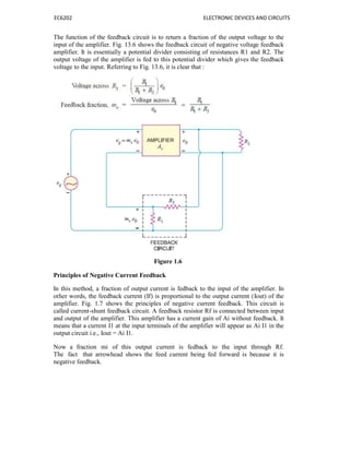
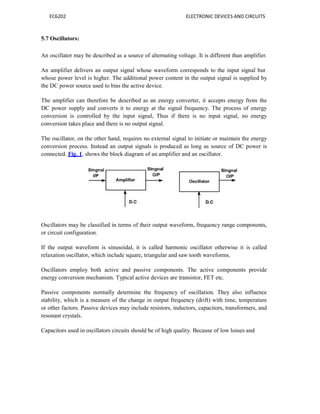
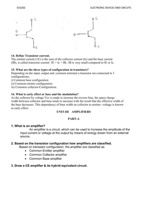
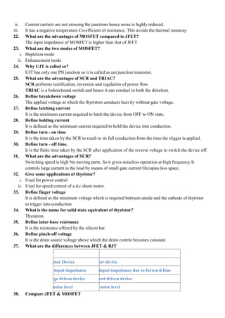
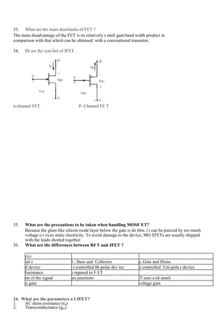
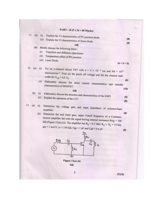
The negative voltage depletion MOSFET.
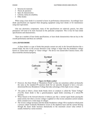
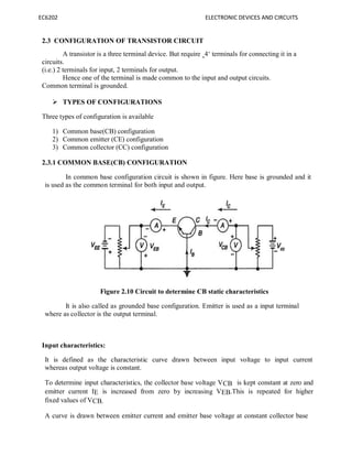
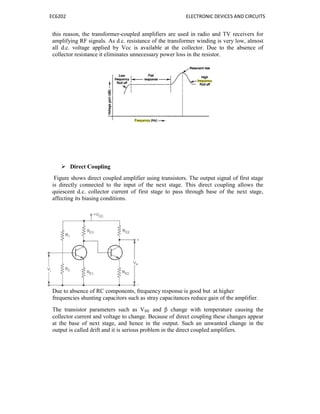
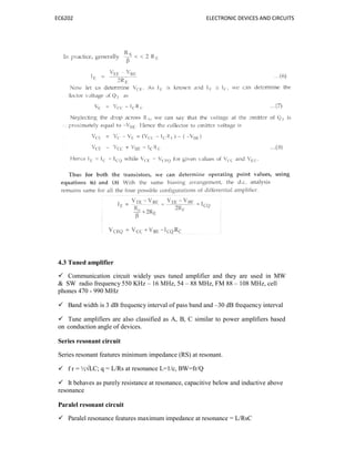
Characteristics curve
Two types
Drain characteristics [ ]
Transfer characteristics [ ]
D-MOSFET‘s are biased to operate in two modes :depletion or enhancement mode.
Figure 3.8 Drain and transfer characteristics
2.5.4 ENHANCEMENT- MODE MOSFET [E-MOSFET]
o In this mode bias on the gate increases the number of charge carriers in the
channel and increases the drain current (ID).
o It operates only in the enhancement mode and has no depletion mode of
operation. It has no physical channel.](https://image.slidesharecdn.com/ec6202edcnotes-170628094019/85/EC6202-ELECTRONIC-DEVICES-AND-CIRCUITS-NOTES-50-320.jpg)


![EC6202 ELECTRONIC DEVICES AND CIRCUITS
9. What are the limitations of h parameters?
The h parameters has the following limitations,
The accurate calculation of h parameters is difficult.
A transistor behaves as a two port network for small signals only, hence h
parameters can be used to analyze only the small signal amplifiers.
10. Why hybrid parameters are called so? Define them?
The dimensions of the hybrid parameters are not alike, that is they are hybrid in
nature so they are called hybrid parameters.
h11 = [ V1/I1] at V2=0; h11 = Inpu,t impedance with output port short circuited.
h12 = [ V1/V2] at I1=0; h12 = Reverse voltage gain with input port open circuited.
h21 = [ I2/I1] at V2=0; h11 = Forward current gain with output port short circuited.
h22 = [I2/V2] at I1=0; h11 = output impedance with input port open circuited.
11. What is transresistance amplifier?
In voltage shunt feedback amplifier the sampled signal is a voltage and the feedback
signal (Which is fed in shunt) is a current.
Rm = Vo / Ii (or) Vo = Rm. Ii
Where, Rm = Amplifier gain.
Vo = Output voltage.
Ii = Input current.
12. What does bootstrapping mean? Why bootstrapping is done in a buffer amplifier?
(Nov, 10)
In the emitter follower amplifier AV tends to unity. If a resistor is connected between input and output
of the emitter follower, the change in the voltage at one end of the resistor changes the voltage at the
other end of the resistor by same value. It is as if resistor is pulling itself up by its bootstraps. Such
effect is known as boot strapping.
13. Draw the Darlington emitter follower circuit. (May,14,13)](https://image.slidesharecdn.com/ec6202edcnotes-170628094019/85/EC6202-ELECTRONIC-DEVICES-AND-CIRCUITS-NOTES-173-320.jpg)
![EC6202 ELECTRONIC DEVICES AND CIRCUITS
14. How can a DC equivalent circuit of an amplifier be obtained?
The analysis of transistor circuits for small signal behaviour can be made by following simple
guidelines. These guidelines are,
Draw the actual circuit diagram
Replace coupling capacitors and emitter bypass capacitor by short circuit
Replace D.C. source by a short circuit
Mark the points B, E, C on the circuit diagram and locate these points as the start of the
equivalent circuit
Replace the transistor by its h-parameter model
15. State Miller’s Theorem. (May,15)
It states that the effect of resistance Z on the input circuit is a ratio of input voltage to the
current which flows from the input to the output.
Z1 =
It states that the effect of resistance Z on the output circuit is the ratio of output
voltage to the current which flows from the output to input.
Z2 =
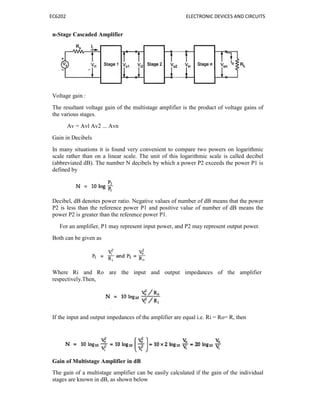
UNIT-IV MULTISTAGE AMPLIFIERS AND DIFFERENTIAL AMPLIFIER
PART-A
1. Mention The Two Applications of tuned amplifiers.[ NOV/DEC 2007, NOV/DEC 2008]
i) They are used in IF amplifiers in Radio and TV receivers.
ii) They are used in wireless communication systems.
2. State two advantages and two disadvantages of tuned amplifiers. [MAY/JUNE 2012]
Advantages:
i) They amplify defined frequencies](https://image.slidesharecdn.com/ec6202edcnotes-170628094019/85/EC6202-ELECTRONIC-DEVICES-AND-CIRCUITS-NOTES-174-320.jpg)
![EC6202 ELECTRONIC DEVICES AND CIRCUITS
15. Define i) Differential gain ii) Common mode gain
The gain with which differential amplifier amplifies the difference between two input signals
is called differential gain of the differential amplifier denoted as A D. The gain with which it amplifies
the common mode signal to produce the output is called common mode gain of the differential
amplifier denoted as A C.
UNIT-V FEEDBACK AMPLIFIERS AND OSCILLATORS
PART-A
1. What is the necessary condition for a Wien bridge oscillator circuit to have sustained
oscillations? [MAY/JUNE 2013]
Then for oscillations to occur in a Wien Bridge Oscillator circuit the following conditions must
apply.
With no input signal the Wien Bridge Oscillator produces output oscillations.
The Wien Bridge Oscillator can produce a large range of frequencies.
The Voltage gain of the amplifier must be at least 3.
The network can be used with a Non-inverting amplifier.
The input resistance of the amplifier must be high compared to R so that the RC network isnot
overloaded and alter the required conditions.
The output resistance of the amplifier must be low so that the effect of external loading is
minimised.
2. Define piezoelectric effect.[MAY/JUNE 2006]
The piezo electric Crystals exhibit a property that if a mechanical stress is applied across one face the
electric potential is developed across opposite face and viceversa. This phenomenon is called piezo
electric effect.
3. Differentiate oscillator from amplifier.[NOV/DEC 2013]
Oscillators Amplifiers
1. They are self-generating circuits. They
generate waveforms like sine, square and
triangular waveforms of their own. Without
having input signal.
1. They are not self-generating
circuits. They need a signal at the
input and they just increase the level
of the input waveform.
2. It have infinite gain 2. It have finite gain
3. Oscillator uses positive feedback. 3. Amplifier uses negative feedback.](https://image.slidesharecdn.com/ec6202edcnotes-170628094019/85/EC6202-ELECTRONIC-DEVICES-AND-CIRCUITS-NOTES-177-320.jpg)
![EC6202 ELECTRONIC DEVICES AND CIRCUITS
4. State Barkhausen criterion for sustained oscillation. What will happen to the oscillation if
the magnitude of the loop gain is greater than unity?[NOV/DEC 2013]
The conditions for oscillator to produce oscillation are given by Barkhausan criterion. They are :
i) The total phase shift produced by the circuit should be 360o or 0o
ii) The Magnitude of loop gain must be greater than or equal to 1 (ie)|Aβ|≥1
In practice loop gain is kept slightily greater than unity to ensure that oscillator work even if there is a
slight change in the circuit parameters.
5. State any two methods of achieving sweep linearity of a time-base
waveform.(NOV/DEC2012)
Exponential charging
Constant current charging
Miller circuit
Bootstrap circuit.
6. Draw the equivalent circuit of a pulse transformer. Name the various elements in
it.(NOV/DEC 2011,NOV/DEC 2009)
R1=Primary winding and source resistance
R2=Total resistance reflected to primary side
=Leakage inductance
L=Magnetizing inductance
C=Total effective shunt capacitance
7. What is the function of time base circuit?(APRIL/MAY 2010)
A linear time base generator produces an output waveform, which produces a
portion which exhibits a linear variation of voltage or current with respect to time.
8. Define feedback. What are the types of it?
The process of combining a fraction or part of output energy back to the input is known
as feedback. The different types of feedback are:
a. Positive feedback, b. Negative feedback
9. What is meant by a) positive feedback b) negative feedback?
Positive feedback
If feedback signal applied is in phase with the input signal and thus increases the input,
it is called as positive feedback. It is also known as regenerative feedback.
Negative feedback
If the feedback signal applied to the input is out of phase with the input signal and thus
signal decrease, it is called negative feedback. It is also known as degenerative feedback.
10. What are the advantages of negative feedback?
It improves the stability of the circuit.
It improves the frequency response of the amplifier.
It improves the percentage of harmonic distortion.](https://image.slidesharecdn.com/ec6202edcnotes-170628094019/85/EC6202-ELECTRONIC-DEVICES-AND-CIRCUITS-NOTES-178-320.jpg)


![. s t
:
lb. (a). (i) Draw the aircuit of a biased positive clipper and explain with
(ii) Draw a hrrghpass:RC eircuit and how it acts as a differentiatg1 ,
',
(8)-:
Or'. :
'.(b)('.Desc1ibe'1heworkingprincip1eof.atransistorized,shuntvoltag9
regulatorwiththehe1pofacircuit]c[iagram. . e
i
(D Explain .the op_e-rationof a Schmitt .trigger circuit and derive
t
3 60526](https://image.slidesharecdn.com/ec6202edcnotes-170628094019/85/EC6202-ELECTRONIC-DEVICES-AND-CIRCUITS-NOTES-227-320.jpg)

The document outlines a course material for EC6202 on electronic devices and circuits, detailing various electronic components such as diodes, transistors, and amplifiers. It covers their structures, operations, characteristics, and applications, structured into five units focusing on pn junction devices, transistors, amplifiers, multistage amplifiers, and feedback amplifiers. The objectives include familiarizing students with electronic devices' structures and enabling them to design applications using these devices.