This document discusses the characteristics and operation of bipolar junction transistors (BJTs). It covers:
- The two types of BJTs - PNP and NPN, which differ in the doping of their layers.
- The three terminals of a BJT - emitter, base, and collector. The base is thinner than the other layers. Emitter injects carriers into the base, and collector collects carriers from the base.
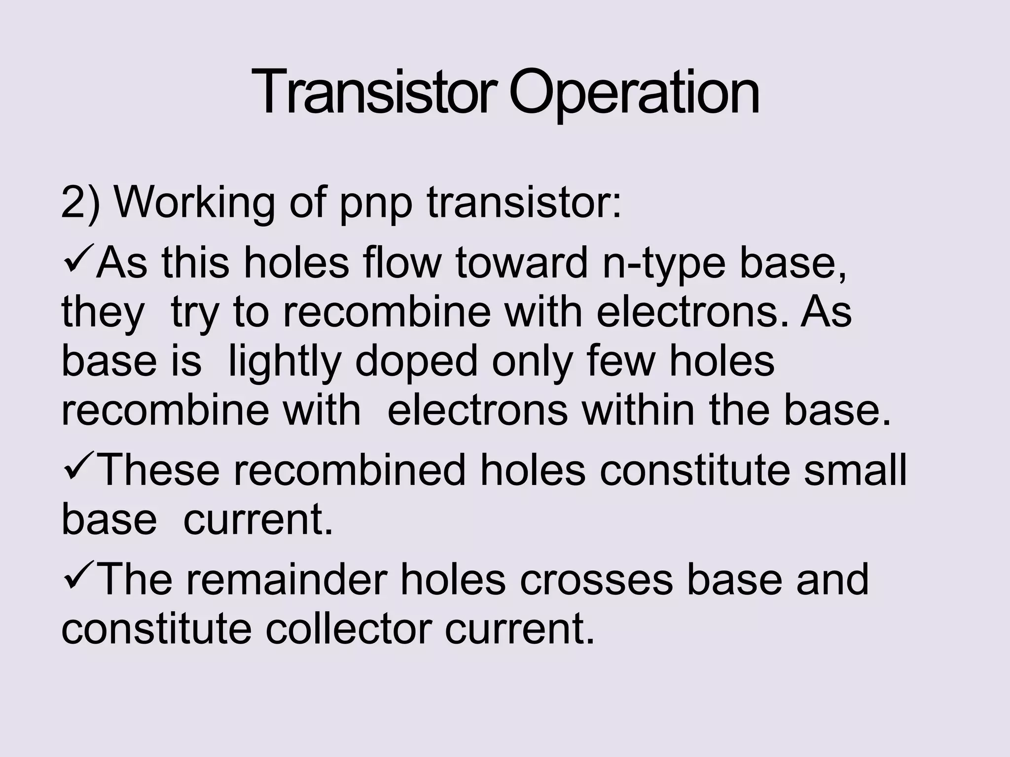
- The operation of NPN and PNP transistors under forward bias of the emitter-base junction and reverse bias of the collector-base junction. Carriers flow from emitter to collector, with a small portion recombining in the base.
-