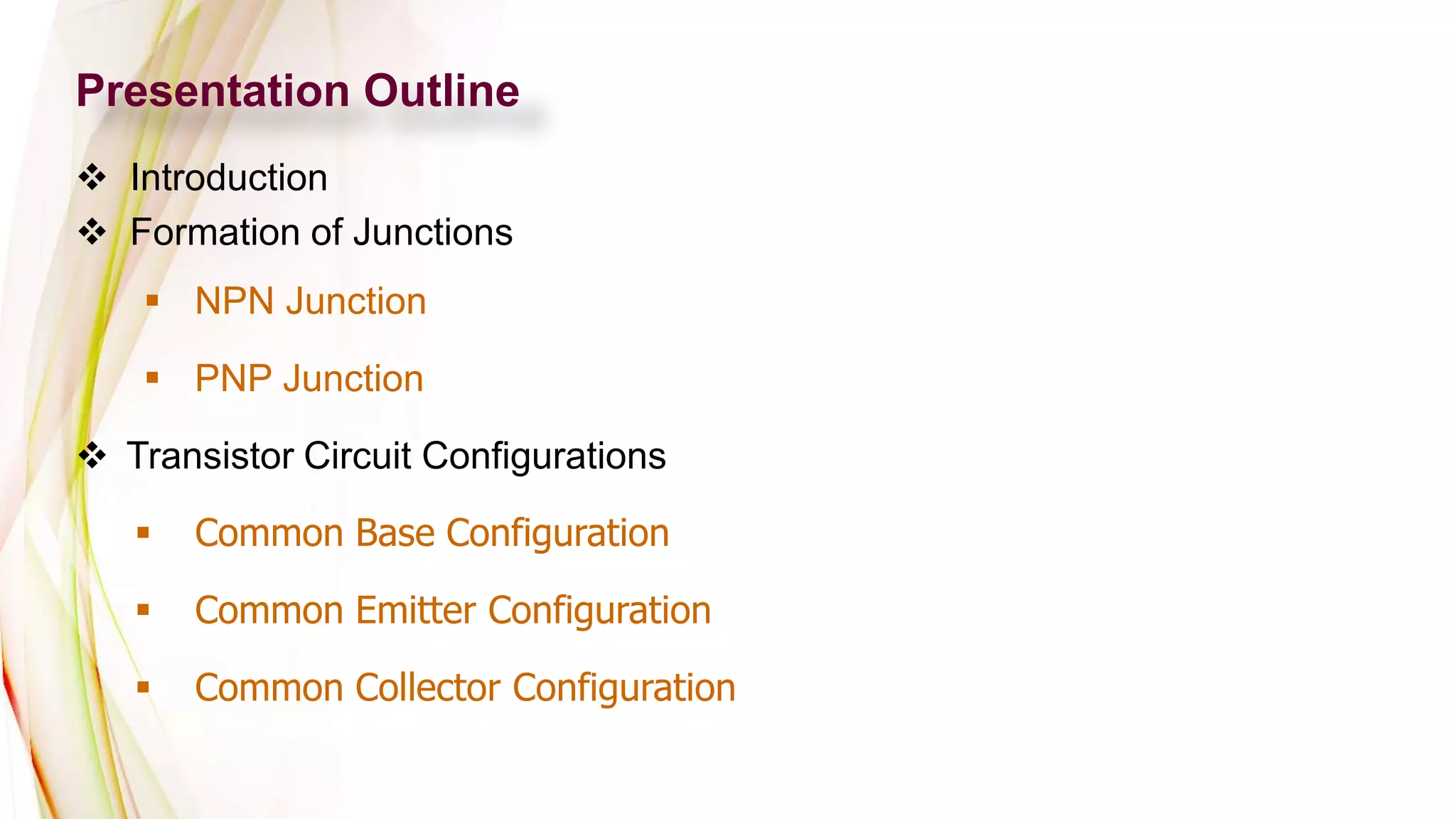
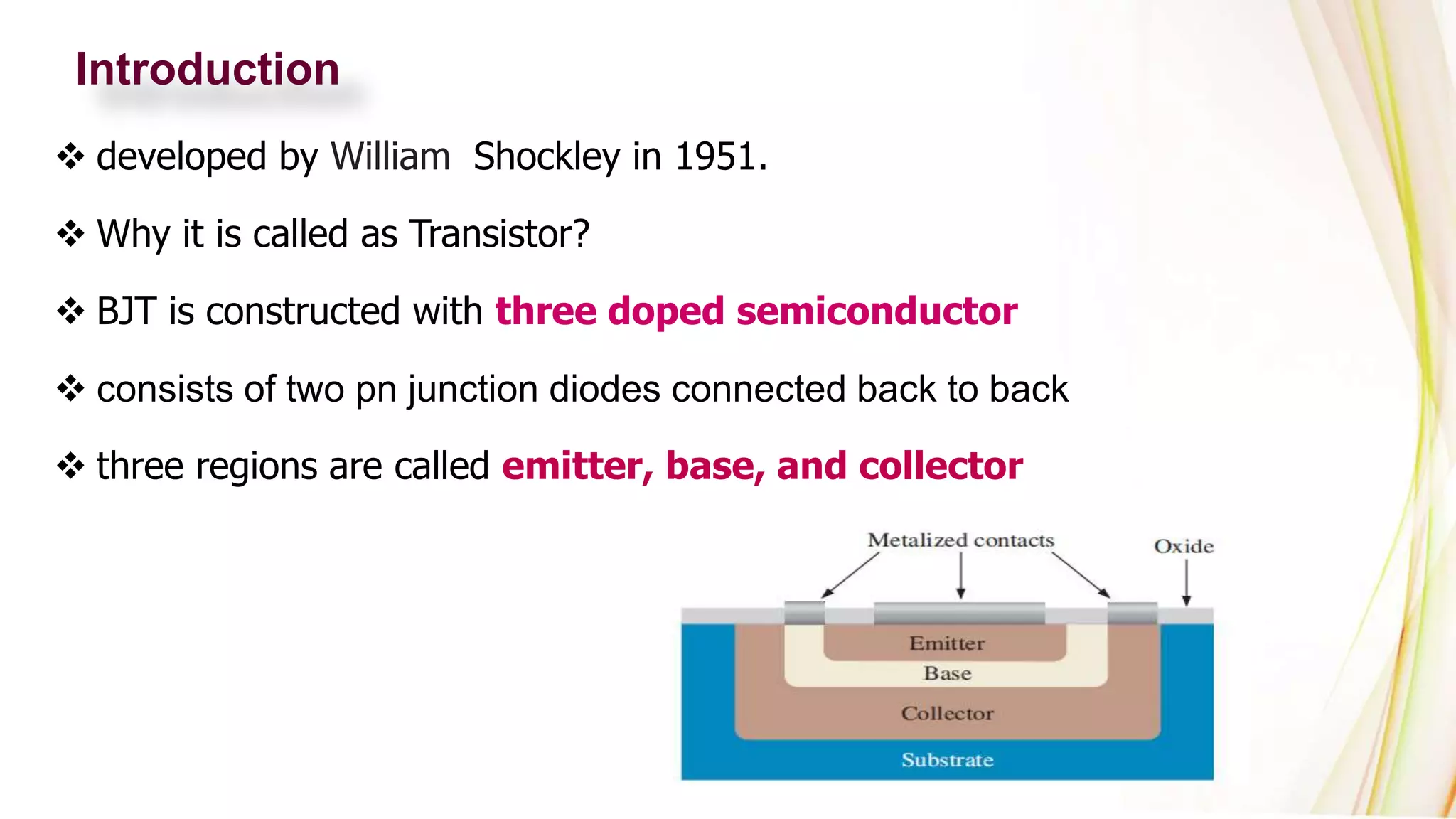
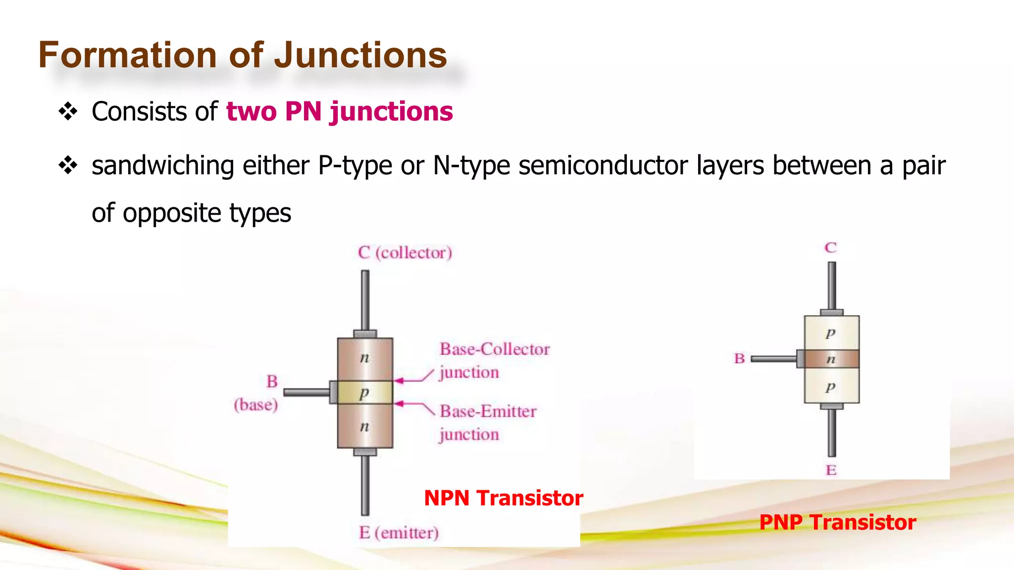
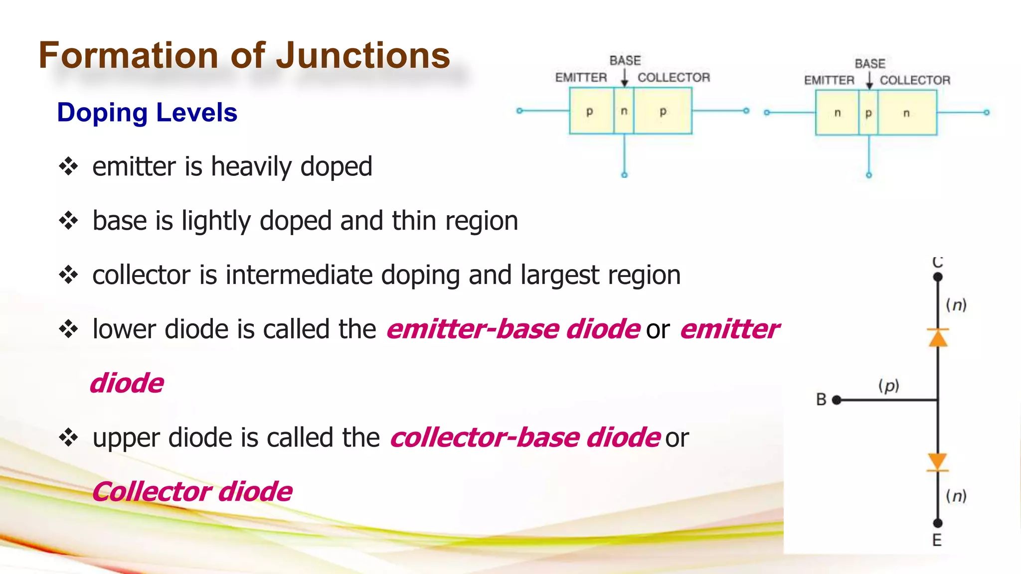
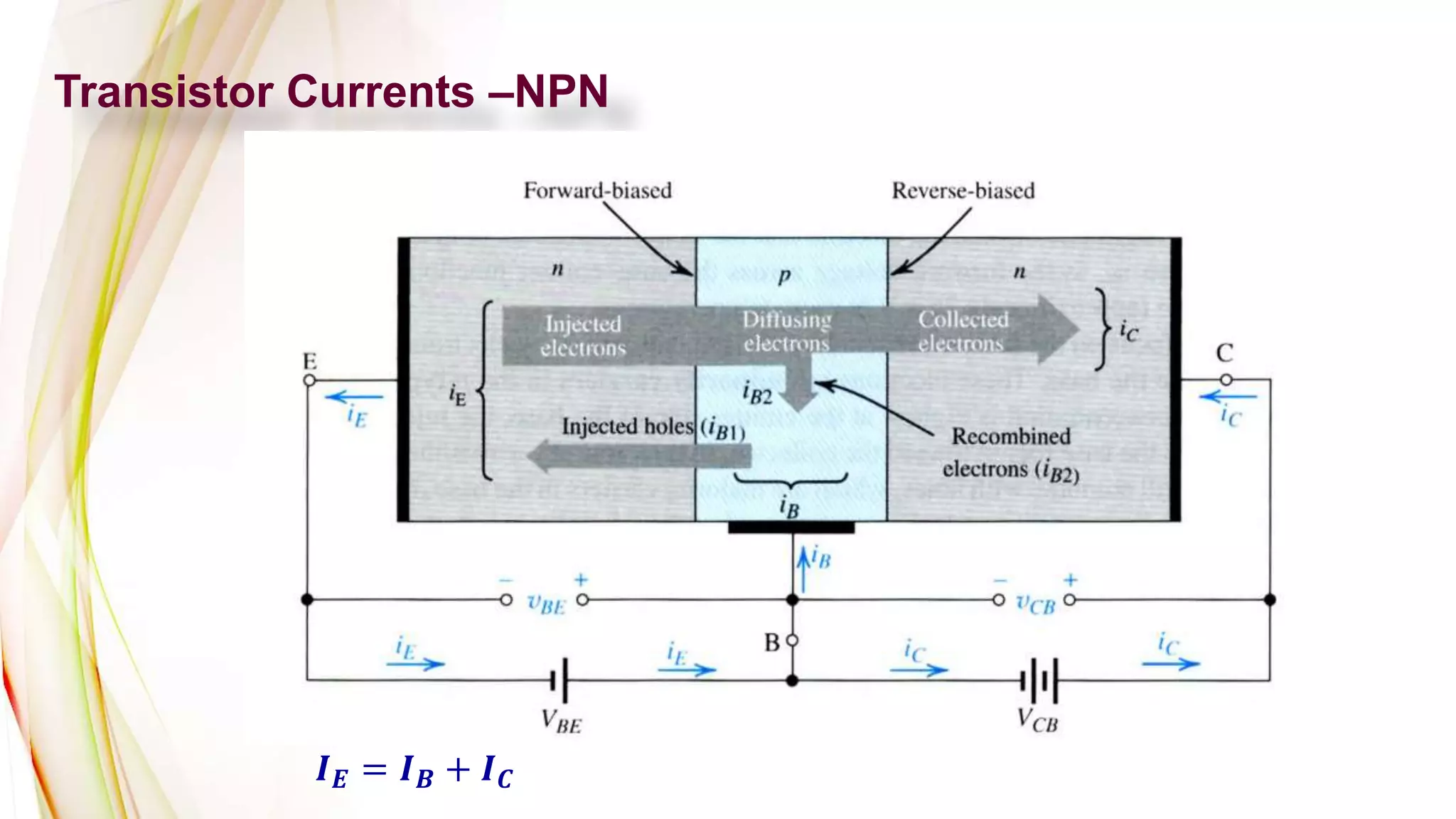
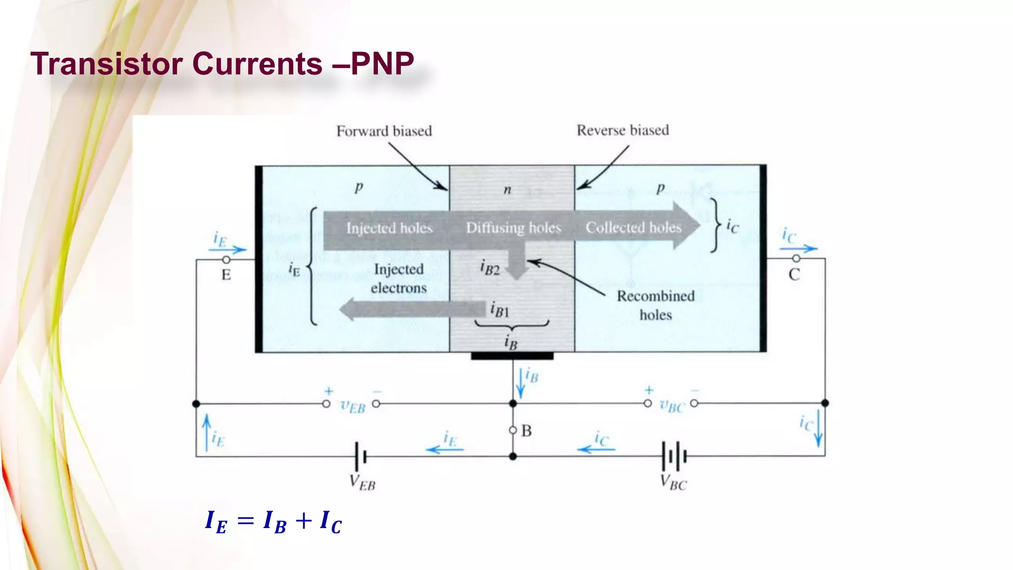
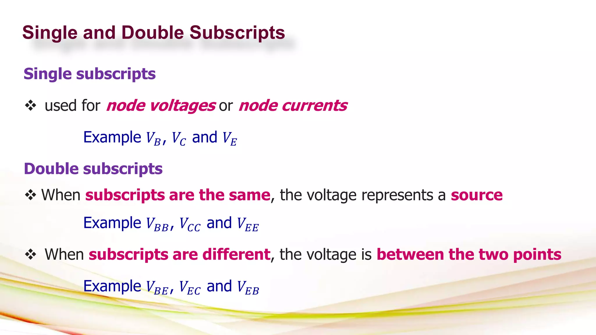
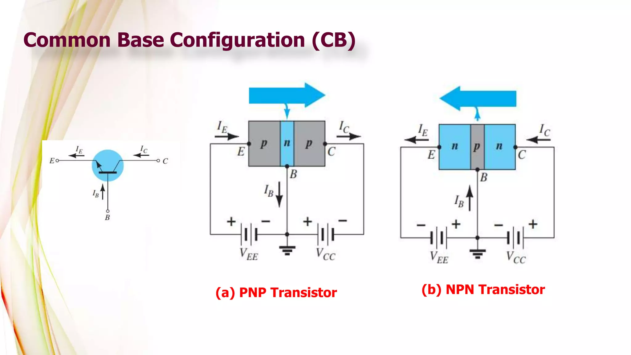
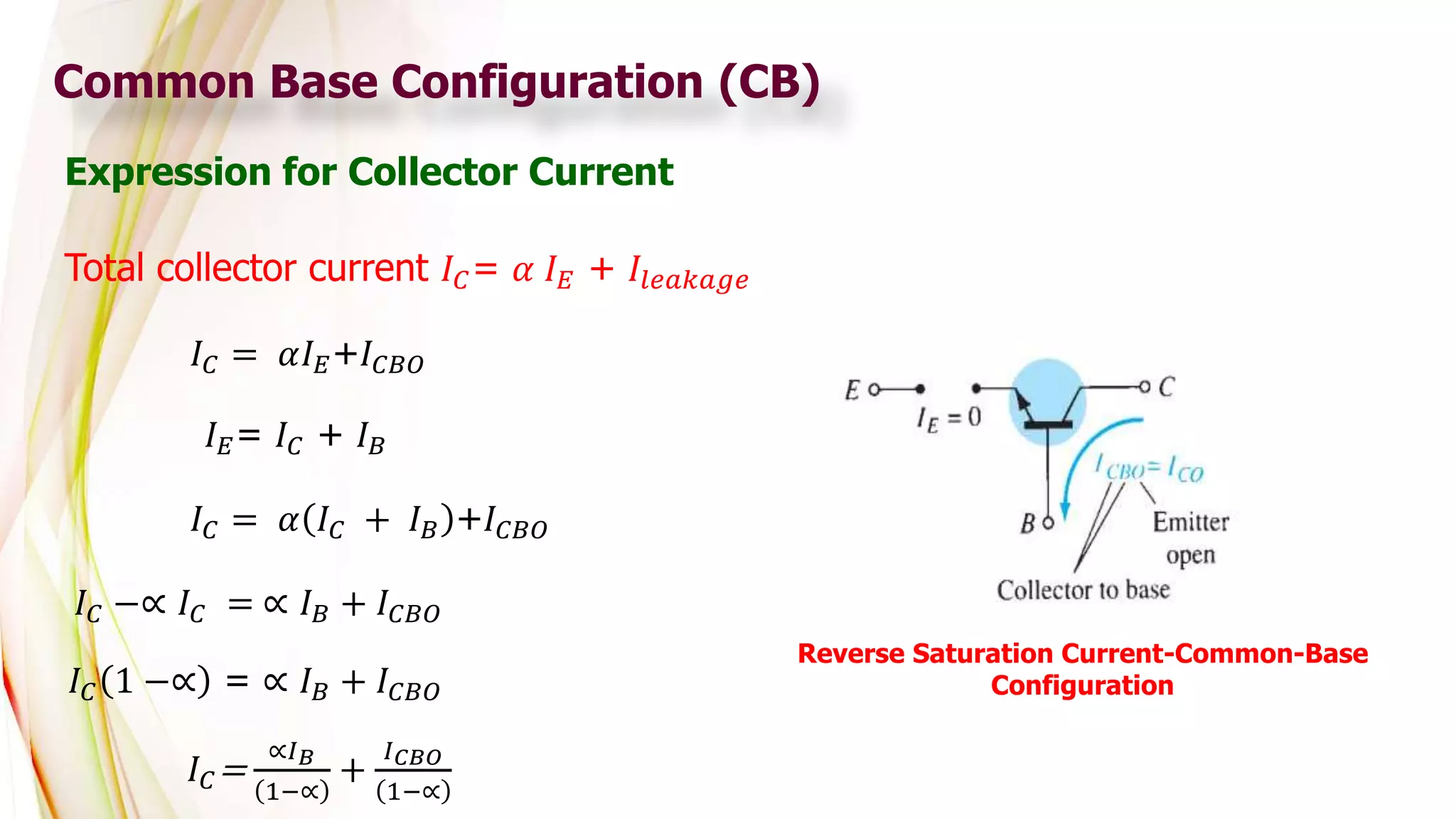
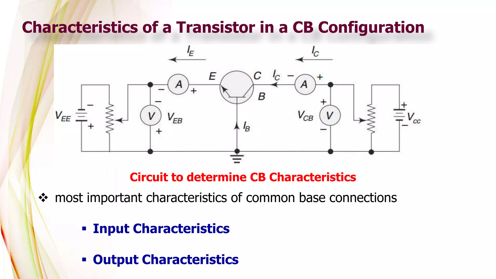
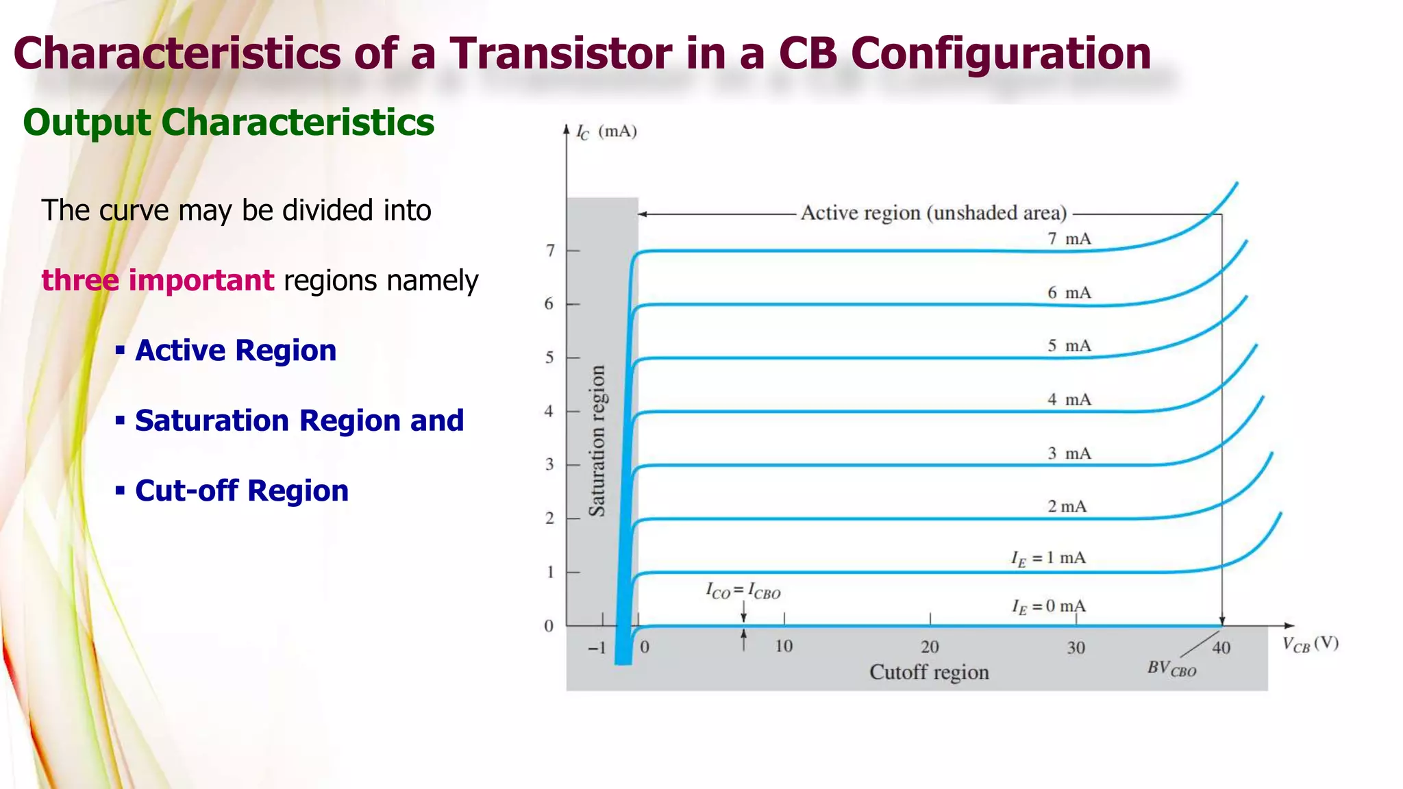
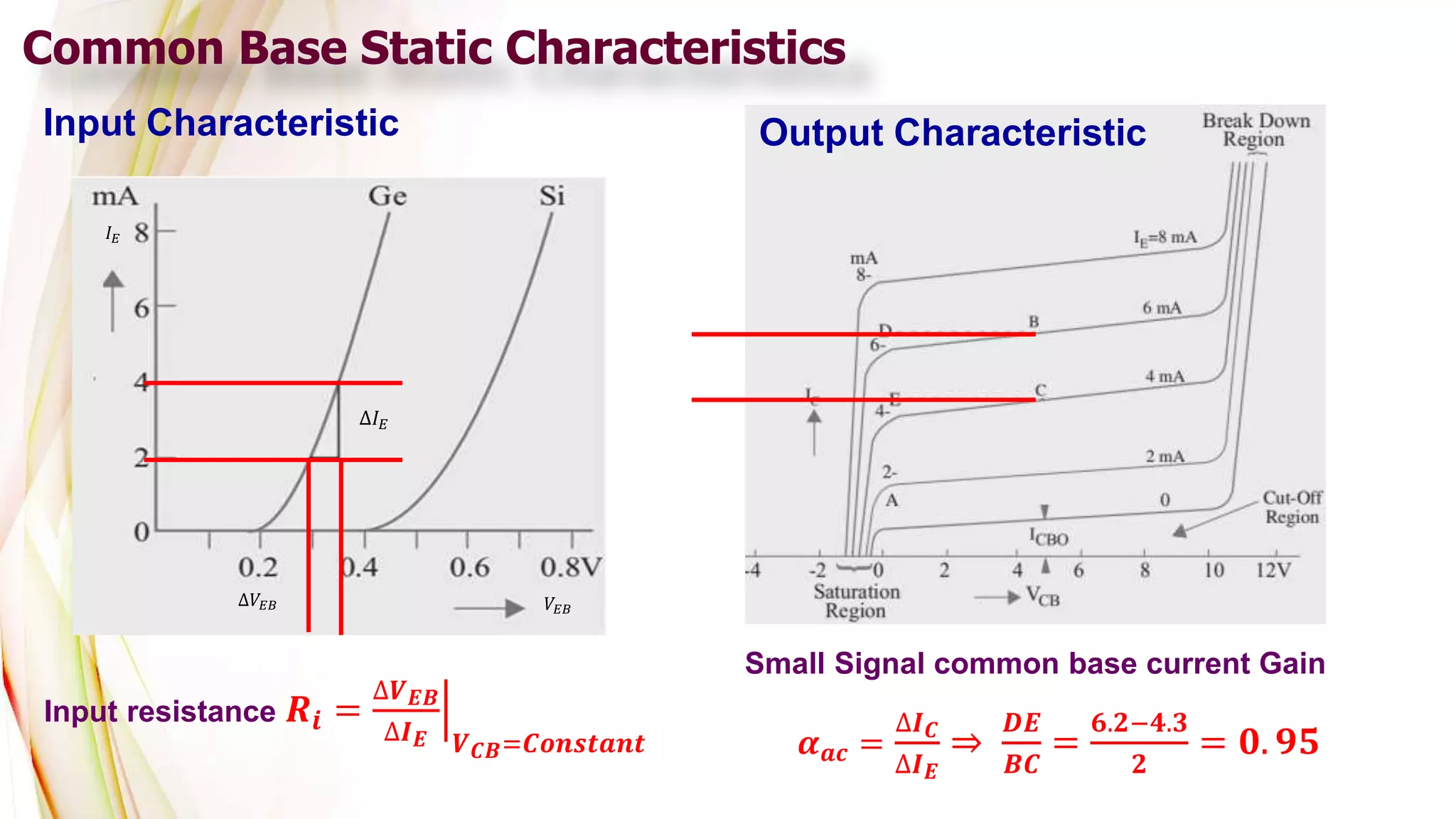
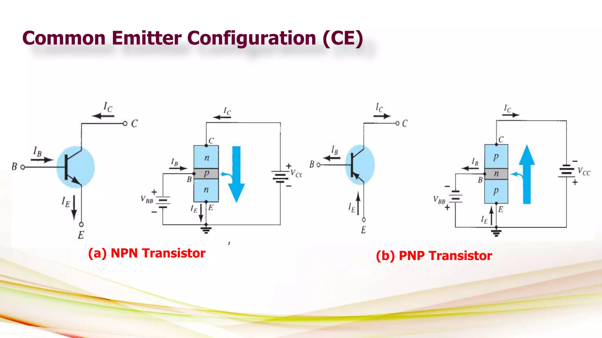
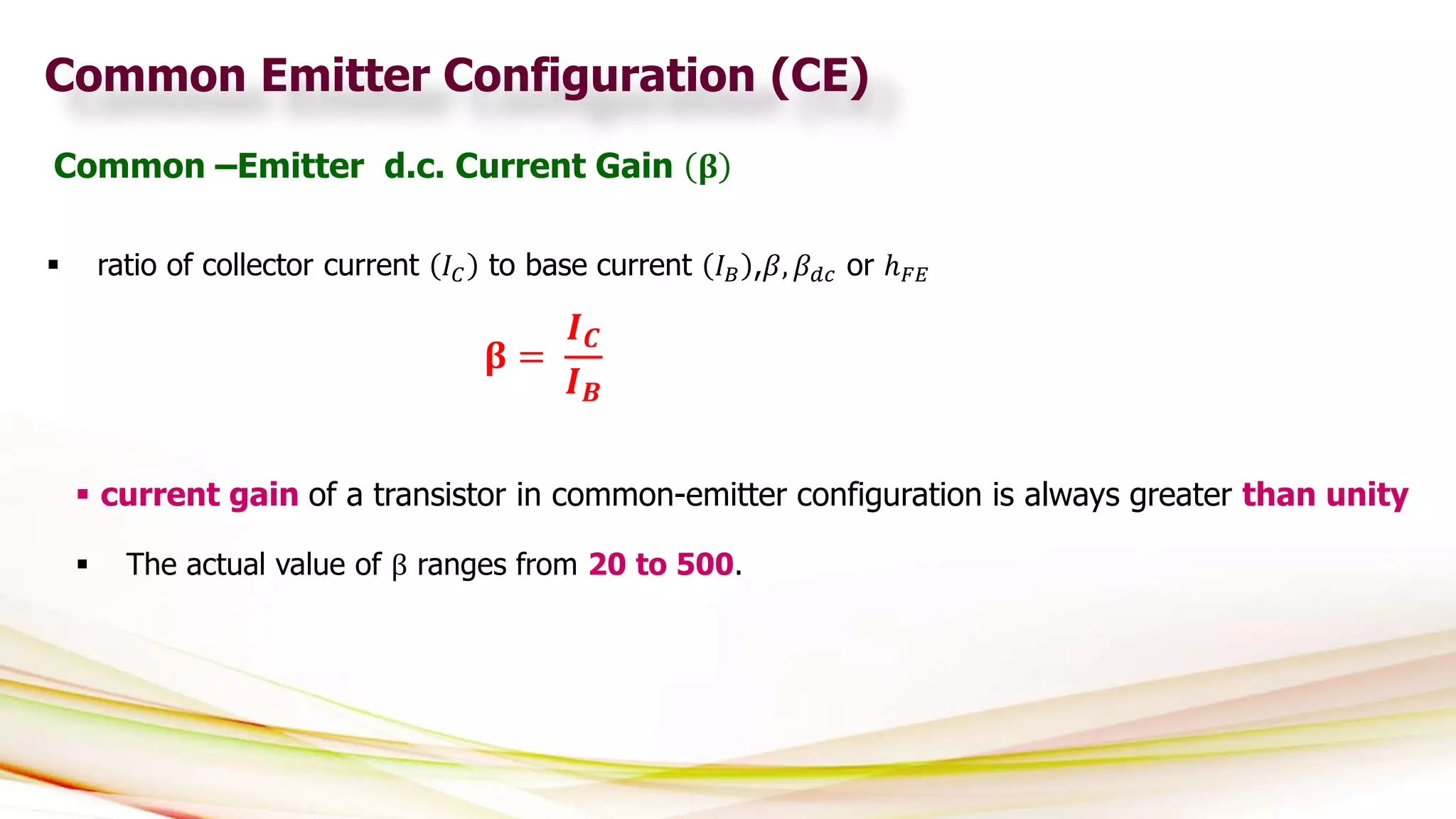
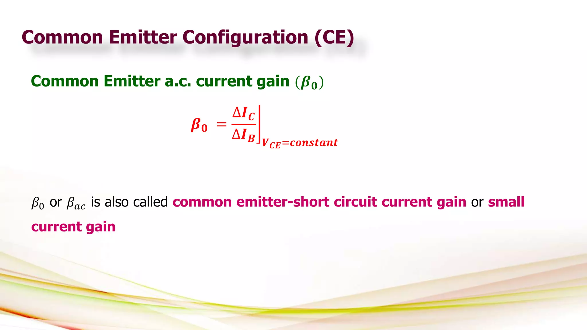
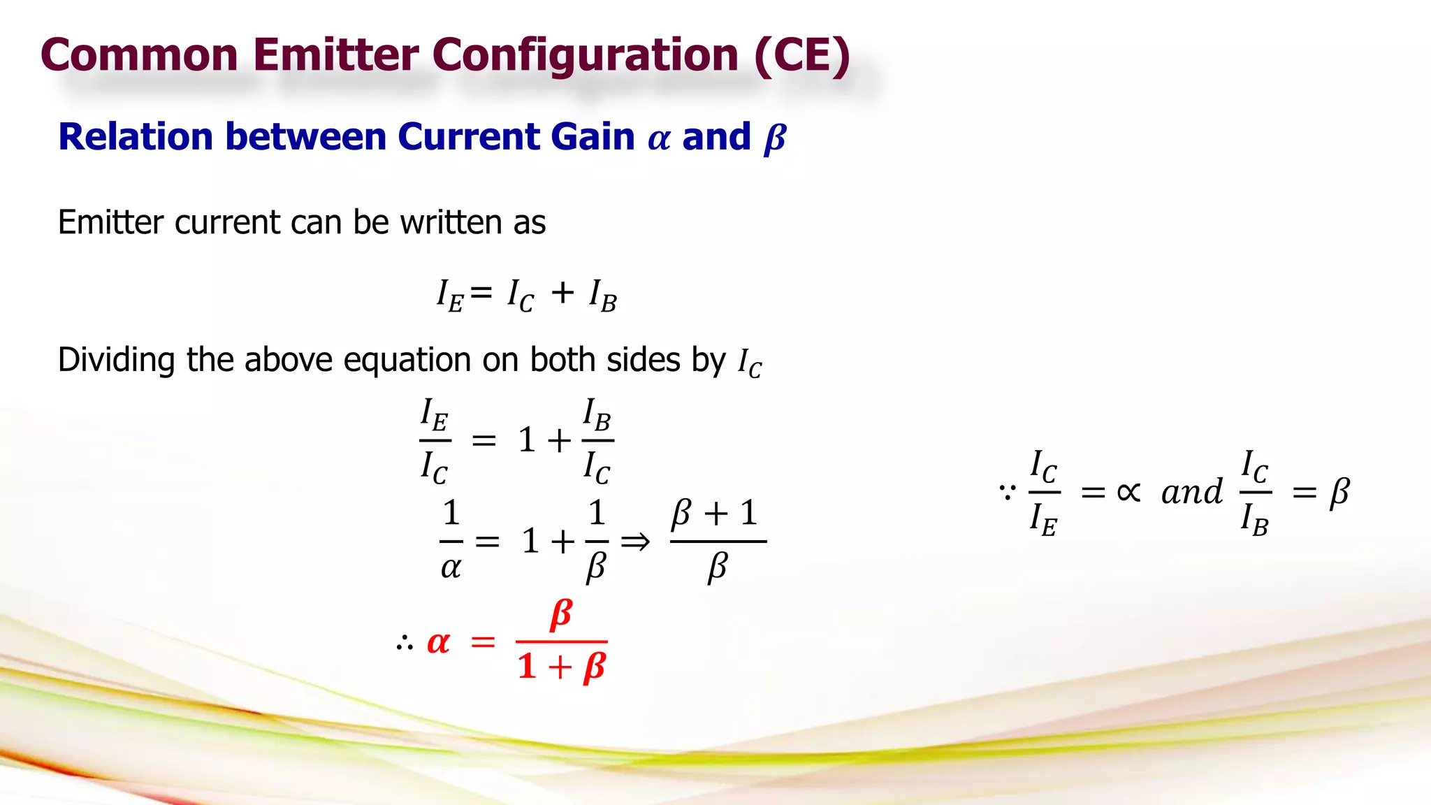
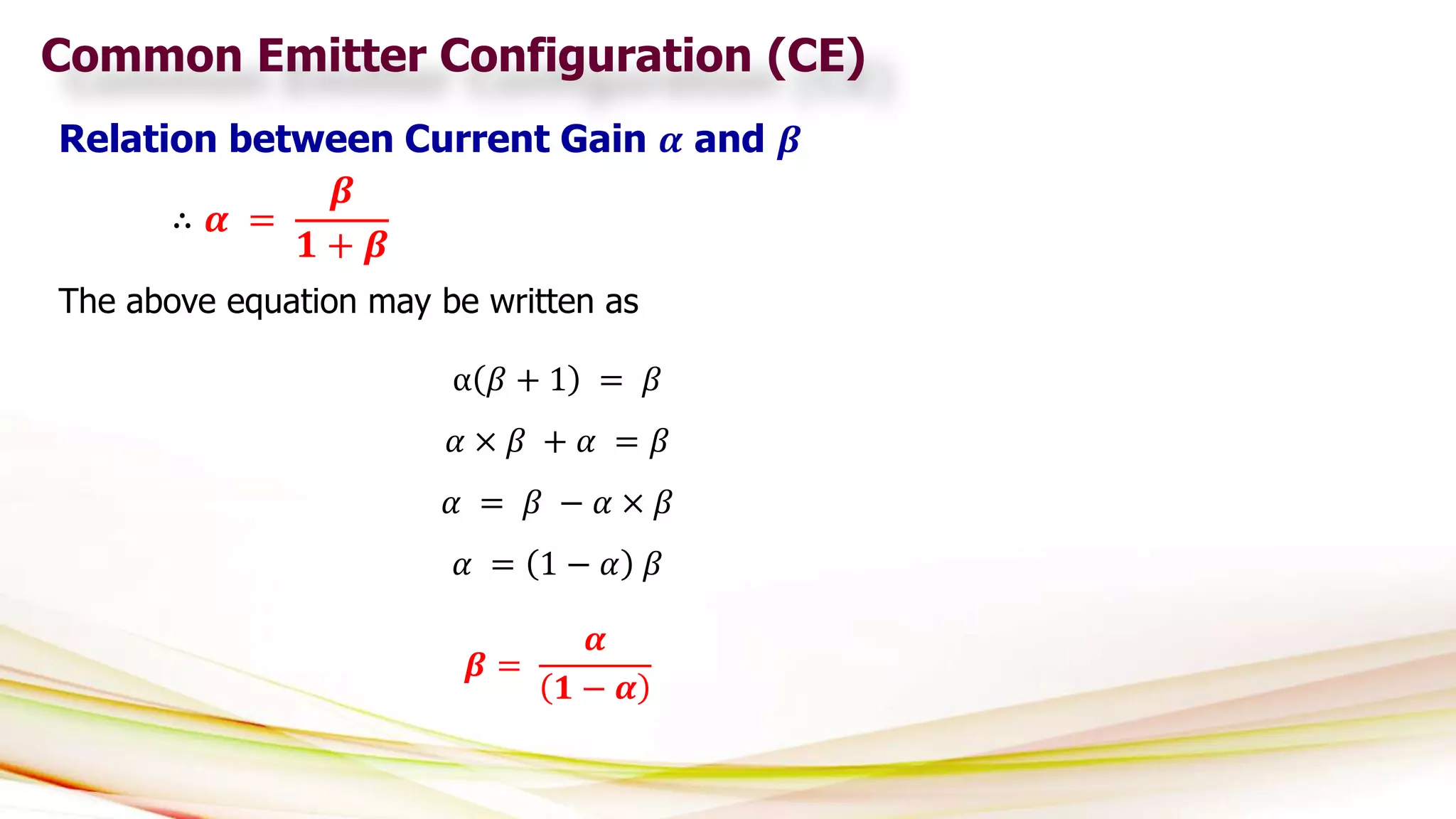
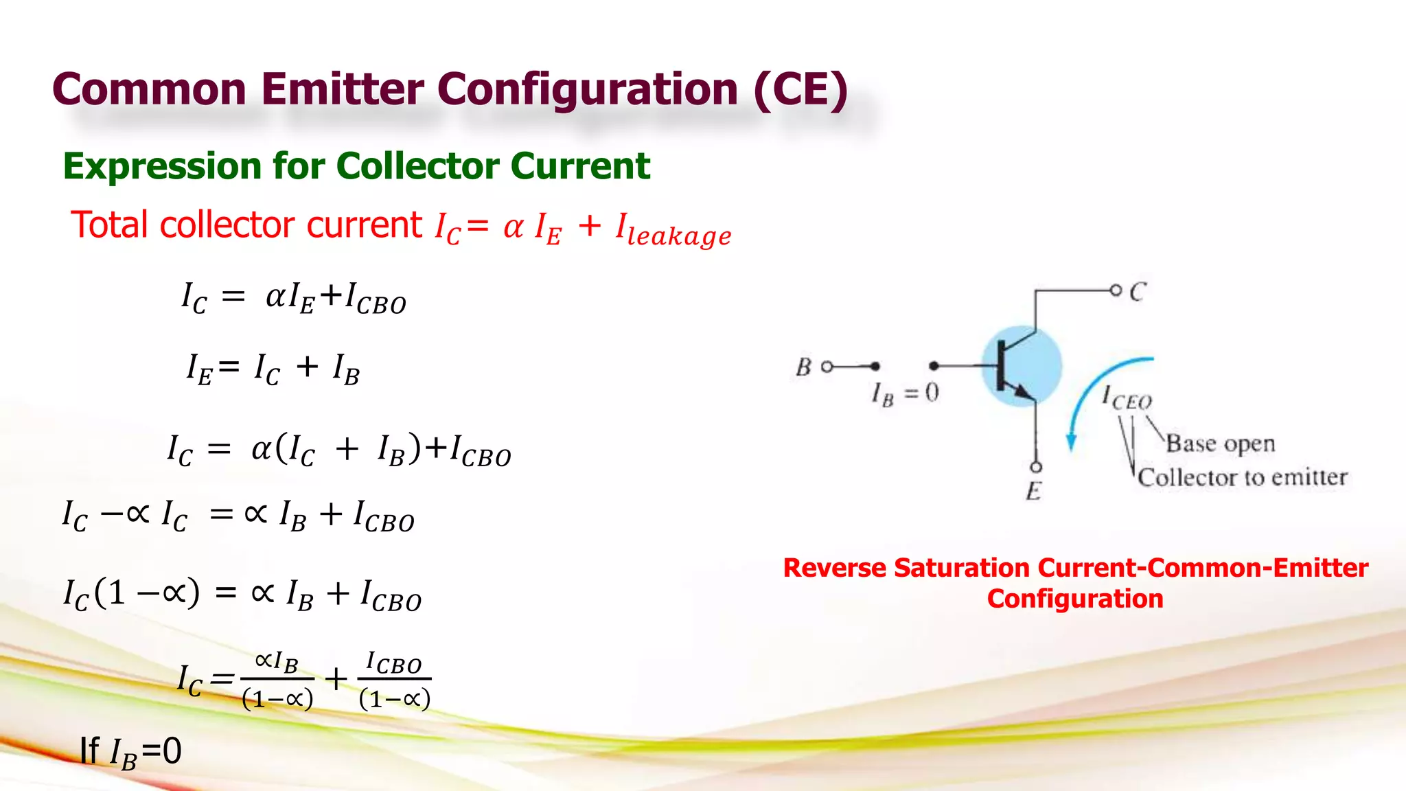
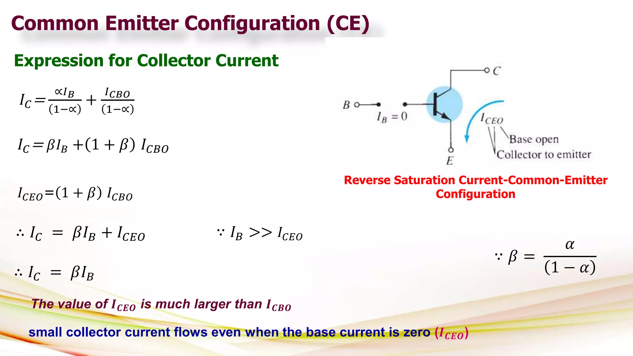
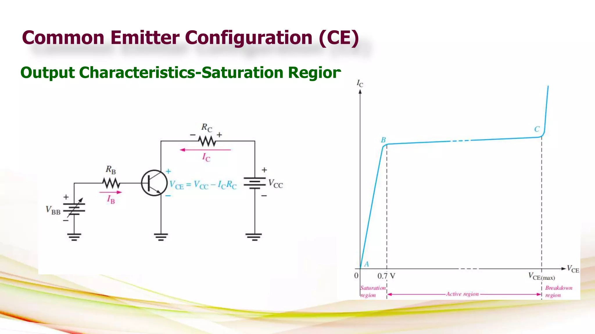
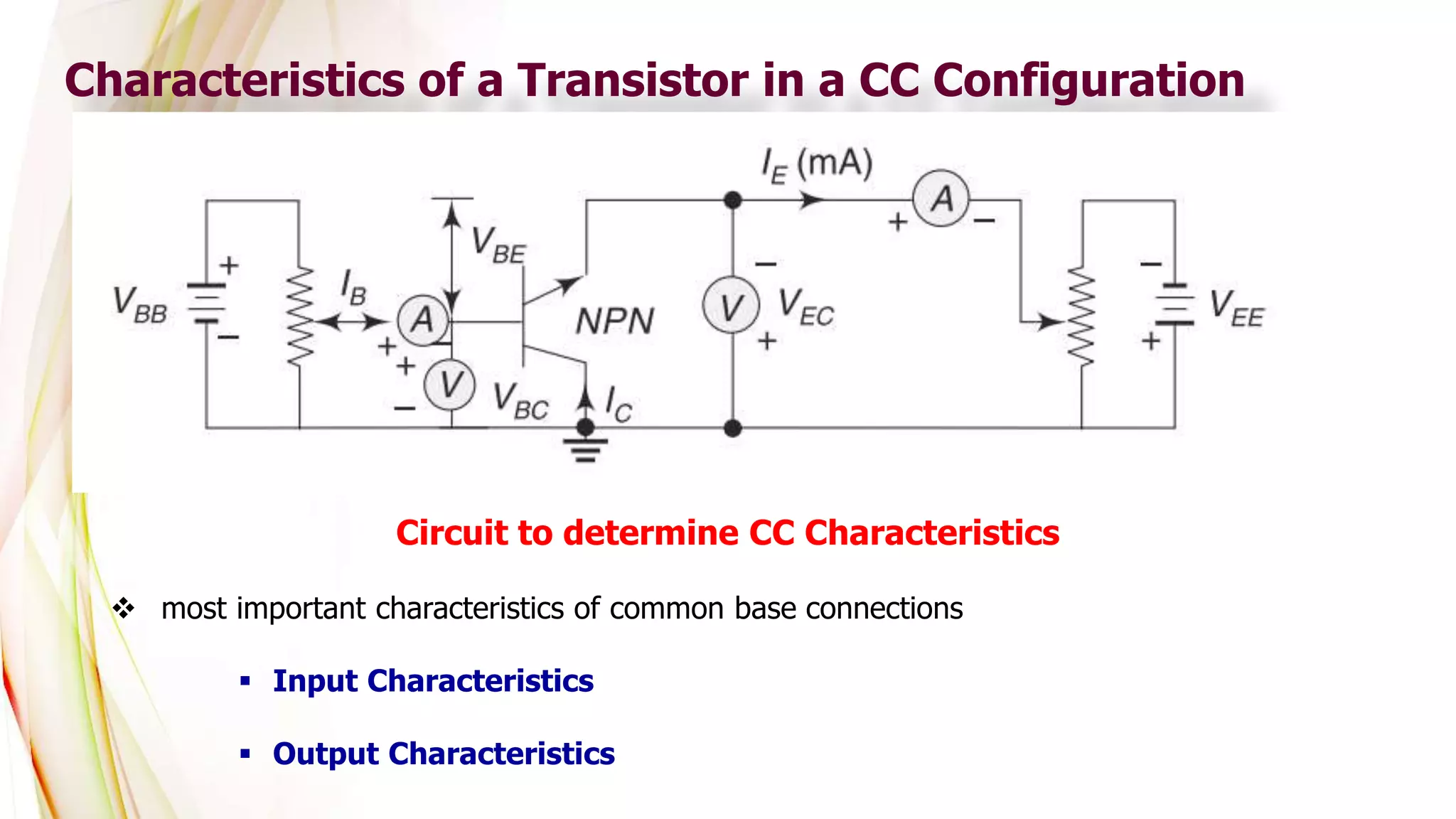
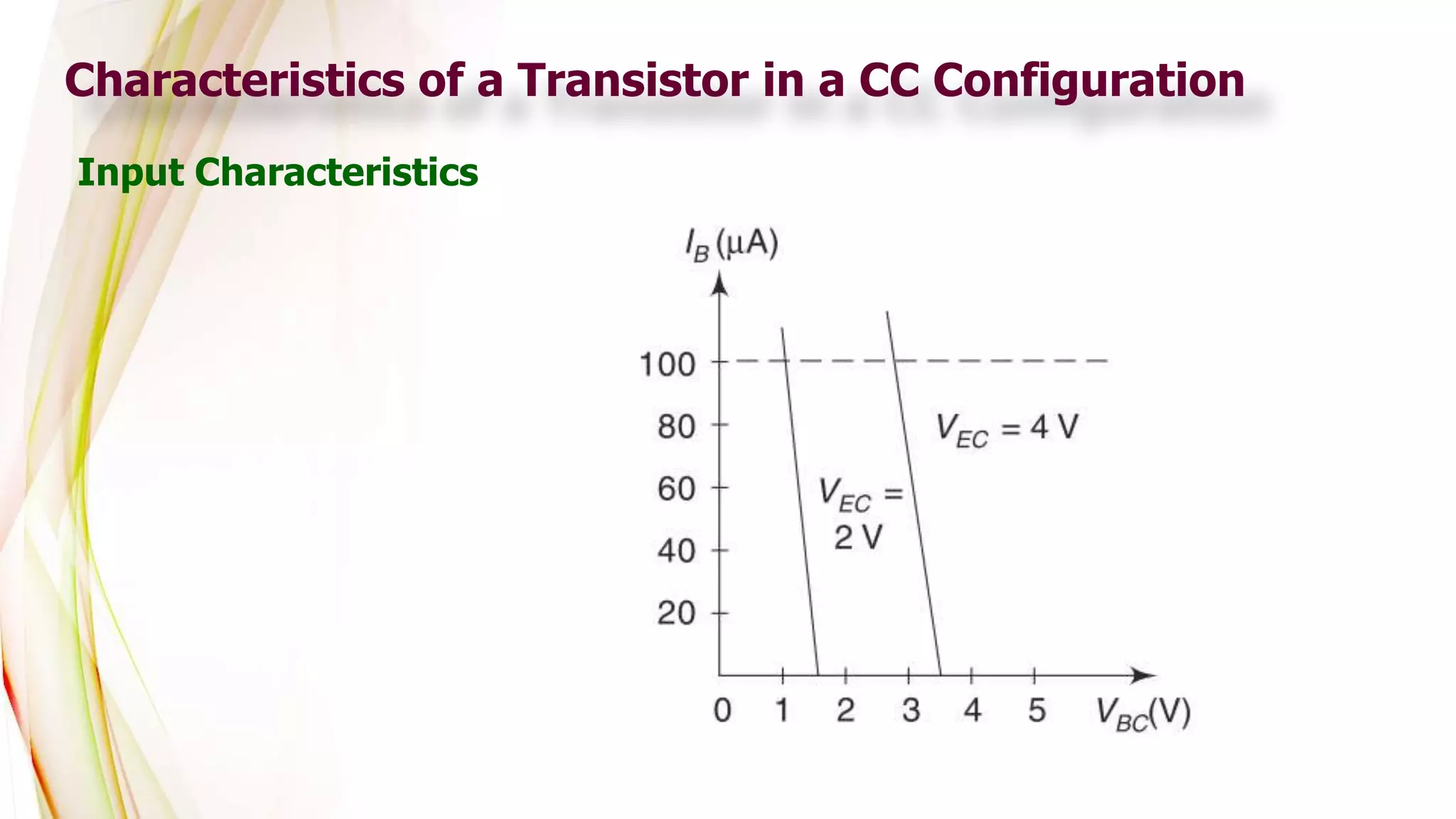
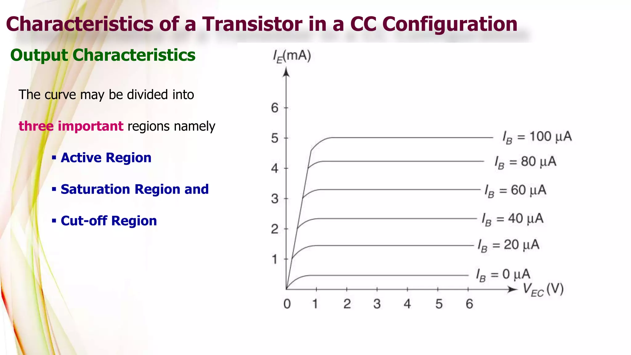
Unit II
Bipolar Junction Transistors
Mr.Darwin Nesakumar A
Assistant Professor/ECE
RMKEC
Presentation Outline
 Introduction
 Formation of Junctions
 NPN Junction
 PNP Junction
 Transistor Circuit Configurations
 Common Base Configuration
 Common Emitter Configuration
 Common Collector Configuration
Presentation Outline
 Transistor Biasing and Stablization
 DC Operating Point and Load Line
 Factors Affecting Stability of Q-Point
 Stability Factor
 Stability Factor of CB Circuit
 Stability Factor of CE Circuit
 Conditions for Proper Biasing of a Transistor
 Methods of Transistor Biasing
Presentation Outline
 Methods of Transistor Biasing
 Base Bias
 Base Bias with Emitter Feedback
 Base Bias with Collector Feedback
 Voltage Divider Bias
 Emitter Bias
Introduction
 developed by William Shockley in 1951.
 Why it is called as Transistor?
 BJT is constructed with three doped semiconductor
 consists of two pn junction diodes connected back to back
 three regions are called emitter, base, and collector
Formation of Junctions
 Consists of two PN junctions
 sandwiching either P-type or N-type semiconductor layers between a pair
of opposite types
PNP Transistor
NPN Transistor
Formation of Junctions
Doping Levels
 emitter is heavily doped
 base is lightly doped and thin region
 collector is intermediate doping and largest region
 lower diode is called the emitter-base diode or emitter
diode
 upper diode is called the collector-base diode or
Collector diode
NPN Transistor – Formation of depletion Layer
Formation of Depletion Layer
Depletion Layer
Operation of NPN Transistor
Electrons in the Base Region
Electrons in the Collector Region
Operation of PNP Transistor
Transistor Currents –NPN
𝑰𝑬 = 𝑰𝑩 + 𝑰𝑪
Transistor Currents –PNP
𝑰𝑬 = 𝑰𝑩 + 𝑰𝑪
Single and Double Subscripts
Single subscripts
 used for node voltages or node currents
Example 𝑉𝐵, 𝑉𝐶 and 𝑉𝐸
Double subscripts
 When subscripts are the same, the voltage represents a source
Example 𝑉𝐵𝐵, 𝑉𝐶𝐶 and 𝑉𝐸𝐸
 When subscripts are different, the voltage is between the two points
Example 𝑉𝐵𝐸, 𝑉𝐸𝐶 and 𝑉𝐸𝐵
 Depending upon the input, output and common terminal, a transistor can
be connected in three configurations.
 Common Base Configuration (CB)
 Common Emitter Configuration (CE)
 Common Collector Configuration (CC)
Transistor Configurations
Common Base Configuration (CB)
(a) PNP Transistor (b) NPN Transistor
Common Base Configuration (CB)
Current Gain or Current Amplification Factor
 ratio of the transistor output current to the input current.
 input current or output current may be either direct current or alternating current
DC current gain
a.c. current gain
Common Base Configuration (CB)
Common -Base d.c. Current Gain (𝜶)
 ratio of collector current 𝐼𝐶 to emitter current 𝐼𝐸 , 𝛼, 𝛼𝑑𝑐 or ℎ𝑓𝐵
𝜶 =
𝑰𝑪
𝑰𝑬
 current gain of a transistor in common-base configuration is always less
than unity
 The actual value of 𝛼 ranges from 0.95 to 0.998.
Common Base Configuration (CB)
Emitter current for CB configuration
𝐼𝐶 = 𝛼. 𝐼𝐸
Emitter current can be written as
𝐼𝐸= 𝐼𝐶 + 𝐼𝐵
= 𝛼. 𝐼𝐸 + 𝐼𝐵
𝐼𝐸 − 𝛼. 𝐼𝐸 = 𝐼𝐵 ⇒ 𝐼𝐸 1 − 𝛼 = 𝐼𝐵
𝑰𝑬 =
𝑰𝑩
𝟏 − 𝜶
Common Base Configuration (CB)
Common Base a.c. current gain (𝜶𝟎)
𝜶𝟎 =
∆𝑰𝑪
∆𝑰𝑬 𝑽𝑪𝑩=𝒄𝒐𝒏𝒔𝒕𝒂𝒏𝒕
𝛼0 is also called common base-short circuit current gain or small current
gain
Common Base Configuration (CB)
Expression for Collector Current
Total collector current 𝐼𝐶= 𝛼 𝐼𝐸 + 𝐼𝑙𝑒𝑎𝑘𝑎𝑔𝑒
Reverse Saturation Current-Common-Base
Configuration
𝐼𝐶 = 𝛼𝐼𝐸+𝐼𝐶𝐵𝑂
𝐼𝐸= 𝐼𝐶 + 𝐼𝐵
𝐼𝐶 = 𝛼 𝐼𝐶 + 𝐼𝐵 +𝐼𝐶𝐵𝑂
𝐼𝐶 −∝ 𝐼𝐶 = ∝ 𝐼𝐵 + 𝐼𝐶𝐵𝑂
𝐼𝐶 1 −∝ = ∝ 𝐼𝐵 + 𝐼𝐶𝐵𝑂
𝐼𝐶=
∝𝐼𝐵
1−∝
+
𝐼𝐶𝐵𝑂
1−∝
Characteristics of a Transistor in a CB Configuration
 most important characteristics of common base connections
 Input Characteristics
 Output Characteristics
Circuit to determine CB Characteristics
Characteristics of a Transistor in a CB Configuration
Input Characteristics
𝑉𝐸𝐵
Characteristics of a Transistor in a CB Configuration
Output Characteristics
The curve may be divided into
three important regions namely
 Active Region
 Saturation Region and
 Cut-off Region
Common Base Static Characteristics
Input Characteristic
Input resistance 𝑹𝒊 =
∆𝑽𝑬𝑩
∆𝑰𝑬 𝑽𝑪𝑩=𝑪𝒐𝒏𝒔𝒕𝒂𝒏𝒕 𝜶𝒂𝒄 =
∆𝑰𝑪
∆𝑰𝑬
⇒
𝑫𝑬
𝑩𝑪
=
𝟔.𝟐−𝟒.𝟑
𝟐
= 𝟎. 𝟗𝟓
Small Signal common base current Gain
Output Characteristic
𝑉𝐸𝐵
∆𝐼𝐸
𝐼𝐸
∆𝑉𝐸𝐵
Common Emitter Configuration (CE)
(a) NPN Transistor (b) PNP Transistor
Common Emitter Configuration (CE)
Current Gain or Current Amplification Factor
 ratio of the transistor output current to the input current.
 input current or output current may be either direct current or alternating current
DC current gain
a.c. current gain
Common –Emitter d.c. Current Gain 𝛃
 ratio of collector current 𝐼𝐶 to base current 𝐼𝐵 ,𝛽, 𝛽𝑑𝑐 or ℎ𝐹𝐸
𝛃 =
𝑰𝑪
𝑰𝑩
 current gain of a transistor in common-emitter configuration is always greater than unity
 The actual value of β ranges from 20 to 500.
Common Emitter Configuration (CE)
Common Emitter a.c. current gain (𝜷𝟎)
𝜷𝟎 =
∆𝑰𝑪
∆𝑰𝑩 𝑽𝑪𝑬=𝒄𝒐𝒏𝒔𝒕𝒂𝒏𝒕
𝛽0 or 𝛽𝑎𝑐 is also called common emitter-short circuit current gain or small
current gain
Common Emitter Configuration (CE)
Relation between Current Gain 𝜶 and 𝜷
Emitter current can be written as
𝐼𝐸= 𝐼𝐶 + 𝐼𝐵
𝐼𝐸
𝐼𝐶
= 1 +
𝐼𝐵
𝐼𝐶
Common Emitter Configuration (CE)
Dividing the above equation on both sides by 𝐼𝐶
∵
𝐼𝐶
𝐼𝐸
= ∝ 𝑎𝑛𝑑
𝐼𝐶
𝐼𝐵
= 𝛽
1
𝛼
= 1 +
1
𝛽
⇒
𝛽 + 1
𝛽
∴ 𝜶 =
𝜷
𝟏 + 𝜷
Relation between Current Gain 𝜶 and 𝜷
Common Emitter Configuration (CE)
∴ 𝜶 =
𝜷
𝟏 + 𝜷
The above equation may be written as
α 𝛽 + 1 = 𝛽
𝛼 × 𝛽 + 𝛼 = 𝛽
𝛼 = 𝛽 − 𝛼 × 𝛽
𝛼 = 1 − 𝛼 𝛽
𝜷 =
𝜶
𝟏 − 𝜶
Expression for Collector Current
Total collector current 𝐼𝐶= 𝛼 𝐼𝐸 + 𝐼𝑙𝑒𝑎𝑘𝑎𝑔𝑒
Reverse Saturation Current-Common-Emitter
Configuration
𝐼𝐶 = 𝛼𝐼𝐸+𝐼𝐶𝐵𝑂
𝐼𝐸= 𝐼𝐶 + 𝐼𝐵
𝐼𝐶 = 𝛼 𝐼𝐶 + 𝐼𝐵 +𝐼𝐶𝐵𝑂
𝐼𝐶 −∝ 𝐼𝐶 = ∝ 𝐼𝐵 + 𝐼𝐶𝐵𝑂
𝐼𝐶 1 −∝ = ∝ 𝐼𝐵 + 𝐼𝐶𝐵𝑂
𝐼𝐶=
∝𝐼𝐵
1−∝
+
𝐼𝐶𝐵𝑂
1−∝
Common Emitter Configuration (CE)
If 𝐼𝐵=0
Expression for Collector Current
𝐼𝐶=
∝𝐼𝐵
1−∝
+
𝐼𝐶𝐵𝑂
1−∝
Common Emitter Configuration (CE)
Reverse Saturation Current-Common-Emitter
Configuration
𝐼𝐶𝐸𝑂= 1 + 𝛽 𝐼𝐶𝐵𝑂
∴ 𝐼𝐶 = 𝛽𝐼𝐵 + 𝐼𝐶𝐸𝑂
∵ 𝛽 =
𝛼
1 − 𝛼
small collector current flows even when the base current is zero (𝑰𝑪𝑬𝑶)
𝐼𝐶= 𝛽𝐼𝐵 + 1 + 𝛽 𝐼𝐶𝐵𝑂
∵ 𝐼𝐵 >> 𝐼𝐶𝐸𝑂
∴ 𝐼𝐶 = 𝛽𝐼𝐵
The value of 𝑰𝑪𝑬𝑶 is much larger than 𝑰𝑪𝑩𝑶
Concept of 𝑰𝑪𝑬𝑶
Common Emitter Configuration (CE)
When the base voltage is applied, then
Base Current = 𝐼𝐵
Collector Current = 𝛽 𝐼𝐵 + 𝐼𝐶𝐸𝑂
Emitter Current = Collector Current + Base Current
Concept of 𝑰𝑪𝑬𝑶
Common Emitter Configuration (CE)
When the base voltage is applied, then
Base Current = 𝐼𝐵
Collector Current = 𝛽 𝐼𝐵 + 𝐼𝐶𝐸𝑂
Emitter Current = Collector Current + Base Current
= 𝛽 𝐼𝐵 + 𝐼𝐶𝐸𝑂 + 𝐼𝐵
= 𝛽 + 1 𝐼𝐵 + 𝐼𝐶𝐸𝑂
As we already know that, 𝐼𝐶𝐸𝑂=
𝐼𝐶𝐵𝑂
1−𝛼
(when 𝐼𝐵 =0)
𝐼𝐶𝐸𝑂 = 1 + 𝛽 𝐼𝐶𝐵𝑂
∵ 𝛽 =
𝛼
1 − 𝛼
∴ 𝛽 + 1 =
1
1 − 𝛼
 most important characteristics of common base connections
 Input Characteristics
 Output Characteristics
Circuit to determine CE Characteristics
Common Emitter Configuration (CE)
Input Characteristics
Common Emitter Configuration (CE)
Output Characteristics
The curve may be divided into
three important regions namely
 Active Region
 Saturation Region and
 Cut-off Region
Common Emitter Configuration (CE)
Output Characteristics-Cutoff Region
Common Emitter Configuration (CE)
Output Characteristics-Saturation Region
Common Emitter Configuration (CE)
Common Emitter Static Characteristics
Input Characteristic
Input resistance 𝑹𝒊 =
∆𝑽𝑩𝑬
∆𝑰𝑩 𝑽𝑪𝑬=𝑪𝒐𝒏𝒔𝒕𝒂𝒏𝒕 𝜷𝒂𝒄 =
∆𝑰𝑪
∆𝑰𝑩
⇒
𝑰𝒄𝟐−𝑰𝒄𝟏
𝑰𝒃𝟐−𝑰𝒃𝟏
=
𝟑.𝟐−𝟐.𝟐 ×𝟏𝟎−𝟑
𝟏𝟎×𝟏𝟎−𝟔 = 𝟏𝟎𝟎
Small Signal common emitter current Gain
Output Characteristic
∆𝑉𝐵𝐸
∆𝐼𝐵
Common Collector Configuration (CC)
(a) PNP Transistor (b) NPN Transistor
Common Collector Configuration (CC)
Current Gain or Current Amplification Factor
 ratio of the transistor output current to the input current.
 input current or output current may be either direct current or alternating current
DC current gain
a.c. current gain
Characteristics of a Transistor in a CC Configuration
 most important characteristics of common base connections
 Input Characteristics
 Output Characteristics
Circuit to determine CC Characteristics
Characteristics of a Transistor in a CC Configuration
Input Characteristics
Characteristics of a Transistor in a CC Configuration
Output Characteristics
The curve may be divided into
three important regions namely
 Active Region
 Saturation Region and
 Cut-off Region
Emitter Injection Efficiency
1. Injected holes from Emitter to Base
2.Holes reaching the reverse biased collector junction
3.Thermally generated electrons and holes making up reverse saturation current
of the collector junction
4. Electrons supplied by the base contact for recombination with holes inject fro
m emitter
5. Electrons injected across the forward biased junction
Emitter Injection Efficiency
𝑉𝐶𝐶
𝑉𝐵𝐵
4
5
1
3
2
P P
N
𝑰𝑬
𝑰𝑩
𝑰𝑪
𝑰𝒑𝑬
𝒆−
flow
𝛾 =
𝐼𝑝𝐸
𝐼𝐸
𝛾 =
𝐼𝑝𝐸
𝐼𝑝𝐸+𝐼𝑛𝐸
If 𝑁𝐸>> 𝑁𝑃, then 𝜸 =1
𝐼𝐸 = 𝐼𝑝𝐸 + 𝐼𝑛𝐸
Base Transport Factor 𝜷∗
𝑉𝐶𝐶
𝑉𝐵𝐵
4
5
1
3
2
P P
N
𝑰𝑬
𝑰𝑩
𝑰𝑪
𝑰𝒑𝑬
𝒆−
flow
𝜷∗ =
𝑶𝒖𝒕𝒑𝒖𝒕 𝒄𝒖𝒓𝒓𝒆𝒏𝒕
𝒊𝒏𝒑𝒖𝒕 𝒄𝒖𝒓𝒓𝒆𝒏𝒕
𝜷∗ =
𝑰𝒑𝑪
𝑰𝒑𝑬
for PNP Transistor
D.C. Load Line
 Input operating point
 Output operating point
D.C. Load Line-Input Operating Point
𝑉𝐵𝐵 − 𝐼𝐵𝑅𝐵 − 𝑉𝐵𝐸 = 0
𝑉𝐵𝐵 − 𝑉𝐵𝐸 = 𝐼𝐵𝑅𝐵
𝑉𝐵𝐵−𝑉𝐵𝐸
𝑅𝐵
= 𝐼𝐵
When x-coordinate is zero
𝑉𝐵𝐸 = 0
𝑉𝐵𝐵
𝑅𝐵
= 𝐼𝐵
𝑷𝟏 is 𝟎,
𝑽𝑩𝑩
𝑹𝑩
D.C. Load Line-Input Operating Point
𝑉𝐵𝐵 − 𝐼𝐵𝑅𝐵 − 𝑉𝐵𝐸 = 0
𝑉𝐵𝐵 − 𝑉𝐵𝐸 = 𝐼𝐵𝑅𝐵
𝑉𝐵𝐵−𝑉𝐵𝐸
𝑅𝐵
= 𝐼𝐵
When y-coordinate is zero
𝐼𝐵 = 0
𝑷𝟐 is 𝑽𝑩𝑩, 𝟎
𝑉𝐵𝐵 − 𝑉𝐵𝐸
𝑅𝐵
= 0 ⇒ 𝑉𝐵𝐵 − 𝑉𝐵𝐸 = 0
D.C. Load Line-Input Operating Point
𝑽𝑩𝑩
𝑹𝑩
D.C. Load Line-Output Operating Point
𝑉𝐶𝐶 − 𝐼𝐶𝑅𝐶 − 𝑉𝐶𝐸 = 0
𝑉𝐶𝐶 − 𝑉𝐶𝐸 = 𝐼𝐶𝑅𝐶
𝑉𝐶𝐶−𝑉𝐶𝐸
𝑅𝐶
= 𝐼𝐶
When x-coordinate is zero
𝑉𝐶𝐸 = 0
𝑉𝐶𝐶
𝑅𝐶
= 𝐼𝐶
𝑷𝟏 is 𝟎,
𝑽𝑪𝑪
𝑹𝑪
D.C. Load Line-Output Operating Point
𝑉𝐶𝐶 − 𝐼𝐶𝑅𝐶 − 𝑉𝐶𝐸 = 0
𝑉𝐶𝐶 − 𝑉𝐶𝐸 = 𝐼𝐶𝑅𝐶
𝑉𝐶𝐶−𝑉𝐶𝐸
𝑅𝐶
= 𝐼𝐶
When y-coordinate is zero
𝐼𝐶 = 0
𝑉𝐶𝐶 − 𝑉𝐶𝐸
𝑅𝐶
= 0 ⇒ 𝑉𝐶𝐶 − 𝑉𝐶𝐸 = 0
𝑉𝐶𝐶 = 𝑉𝐶𝐸
𝑷𝟐 is 𝑽𝑪𝑪, 𝟎
D.C. Load Line-Output Operating Point
Position of Q-Point
Operating Point Nearer to Cut-Off Region
Position of Q-Point
Operating Point Nearer to Saturation Region
Position of Q-Point
Operating Point at the Active Region
DC Biasing
Need for Biasing
 operate the transistor in the desired region
 output signal power greater than the input signal power.
Factors affecting Stability of Q – Point
Mainly due to transistor parameters 𝛽
𝑰𝑪 = 𝜷. 𝑰𝑩 + 𝟏 + 𝜷 . 𝑰𝑪𝑶
Stability Factor
(𝑖)𝑺 =
𝝏𝑰𝑪
𝝏𝑰𝑪𝑶
𝜷 𝒂𝒏𝒅 𝑰𝑩 𝒂𝒔 𝒄𝒐𝒏𝒔𝒕𝒂𝒏𝒕
(ii) Stability factor can be obtained from the collector current equation
𝐼𝐶 = 𝛽. 𝐼𝐵 + 1 + 𝛽 . 𝐼𝐶𝑂
Differentiating the above expression w.r.t 𝐼𝐶
1 =
𝜕 𝛽. 𝐼𝐵
𝜕𝐼𝐶
+
𝜕 1 + 𝛽 . 𝐼𝐶𝑂
𝜕𝐼𝐶
1 =
𝛽𝜕 𝐼𝐵
𝜕𝐼𝐶
+ 1 + 𝛽
𝜕. 𝐼𝐶𝑂
𝜕𝐼𝐶
Stability Factor
1 =
𝛽𝜕 𝐼𝐵
𝜕𝐼𝐶
+ 1 + 𝛽
𝜕. 𝐼𝐶𝑂
𝜕𝐼𝐶
1=
𝛽𝜕 𝐼𝐵
𝜕𝐼𝐶
+ 1 + 𝛽
1
𝑆
∵ 𝑆 =
𝜕𝐼𝐶
𝜕𝐼𝐶𝑂
1−
𝛽𝜕 𝐼𝐵
𝜕𝐼𝐶
= 1 + 𝛽
1
𝑆
𝑺 =
𝟏 + 𝜷
𝟏 − 𝜷
𝝏 𝑰𝑩
𝒅𝑰𝑪
Stability Factor of Common Base Circuit
𝐼𝐶 = 𝛼. 𝐼𝐸 + 𝐼𝐶𝑂
Differentiating the above equation with respect to 𝐼𝐶
1 = 𝛼. 0 +
𝜕𝐼𝐶𝑂
𝜕𝐼𝐶
1=
1
𝑆
∴ 𝑺 = 𝟏
∵ 𝑆 =
𝜕𝐼𝐶
𝜕𝐼𝐶𝑂
stability factor indicates that the common base circuits are highly stable.
Stability Factor of Common Emitter Circuit
𝑆 =
𝜕𝐼𝐶
𝜕𝐼𝐶𝑂
𝐼𝐶 = 𝛽. 𝐼𝐵 + 1 + 𝛽 . 𝐼𝐶𝑂
Differentiating the above equation with respect to 𝐼𝐶
1 = 𝛽. 0 + 1 + 𝛽 .
𝜕𝐼𝐶𝑂
𝜕𝐼𝐶
1 =
1 + 𝛽
𝑆
∴ 𝑆 = 1 + 𝛽
collector current is highly dependent upon the reverse saturation current
Methods of Transistor Biasing
Base bias or Fixed Current bias
Base bias with emitter feedback
Base bias with collector–feedback resistor
Base bias with collector and emitter feedback
Emitter bias
Voltage Divider bias
• Base bias or Fixed Current bias
𝑉𝐶𝐶 = 𝐼𝐵𝑅𝐵 + 𝑉𝐵𝐸
𝑉𝐶𝐶 − 𝑉𝐵𝐸 = 𝐼𝐵𝑅𝐵
𝐼𝐵 =
𝑉𝐶𝐶 − 𝑉𝐵𝐸
𝑅𝐵
If 𝑉𝐵𝐸 << 𝑉𝐶𝐶
𝐼𝐵 =
𝑉𝐶𝐶
𝑅𝐵
Base bias or Fixed Current bias
Collector Emitter Loop
𝑉𝐶𝐶 = 𝐼𝐶. 𝑅𝐶 + 𝑉𝐶𝐸
𝑽𝑪𝑪 − 𝑰𝑪. 𝑹𝑪 = 𝑽𝑪𝑬
Calculate the Output Current and Voltage
𝐼𝐶 = 𝛽𝐼𝐵
𝑰𝑪 = 𝜷
𝑽𝑪𝑪
𝑹𝑩
Stability Factor of Base-Bias Circuit
𝐒 = 𝟏 + 𝜷
Base bias with Emitter Feedback
(a)
(b)
Base bias with Emitter Feedback
Base–Emitter Loop 𝑉𝐶𝐶 − 𝑅𝐵𝐼𝐵 − 𝑉𝐵𝐸 − 𝐼𝐸𝑅𝐸 = 0
𝐼𝐸 = 𝐼𝐵 + 𝐼𝐶
𝐼𝐸 = 𝐼𝐵 + 𝛽𝐼𝐵
𝐼𝐸 = 𝐼𝐵 1 + 𝛽
𝑉𝐶𝐶 − 𝑉𝐵𝐸 = 𝑅𝐵𝐼𝐵 + 𝐼𝐵 1 + 𝛽 𝑅𝐸
𝑉𝐶𝐶 − 𝑉𝐵𝐸 = 𝑅𝐵 + 1 + 𝛽 𝑅𝐸 𝐼𝐵
𝑰𝑩 =
𝑽𝑪𝑪−𝑽𝑩𝑬
𝑹𝑩+ 𝟏+𝜷 𝑹𝑬
Base bias with Emitter Feedback
Base–Emitter Loop 𝑰𝑩 =
𝑽𝑪𝑪−𝑽𝑩𝑬
𝑹𝑩+ 𝟏+𝜷 𝑹𝑬
Let 1 + 𝛽 = 𝛽
𝐼𝐵 =
𝑉𝐶𝐶 − 𝑉𝐵𝐸
𝑅𝐵 + 𝛽𝑅𝐸
Base bias with Emitter Feedback
Collector–Emitter Loop Calculate the Output Current and Voltage
𝑉𝐶𝐶 = 𝑅𝐶𝐼𝐶 + 𝑉𝐶𝐸 + 𝐼𝐸𝑅𝐸
𝑉𝐶𝐶 − 𝑅𝐶𝐼𝐶 − 𝐼𝐸𝑅𝐸 = 𝑉𝐶𝐸
∵ 𝐼𝐸⋍ 𝐼𝐶
𝑉𝐶𝐶 − 𝑅𝐶𝐼𝐶 − 𝐼𝐶𝑅𝐸 = 𝑉𝐶𝐸
𝑉𝐶𝐶 − 𝐼𝐶 𝑅𝐶 + 𝑅𝐸 = 𝑉𝐶𝐸
Base bias with Emitter Feedback
Stability Factor of Base-Bias with Emitter Feedback
𝑉𝐶𝐶 − 𝑅𝐵𝐼𝐵 − 𝑉𝐵𝐸 − 𝐼𝐸𝑅𝐸 = 0
Replacing 𝐼𝐸 = 𝐼𝐵 + 𝐼𝐶, in the above expression
𝑉𝐶𝐶 − 𝑅𝐵𝐼𝐵 − 𝑉𝐵𝐸 − 𝐼𝐵 + 𝐼𝐶 𝑅𝐸 = 0
𝑉𝐶𝐶 − 𝐼𝐵 𝑅𝐵 + 𝑅𝐸 − 𝑉𝐵𝐸 − 𝐼𝐶𝑅𝐸 = 0
𝑉𝐶𝐶 − 𝑉𝐵𝐸 − 𝐼𝐶𝑅𝐸 = 𝐼𝐵 𝑅𝐵 + 𝑅𝐸
𝑉𝐶𝐶 − 𝑉𝐵𝐸 − 𝐼𝐶𝑅𝐸
𝑅𝐵 + 𝑅𝐸
= 𝐼𝐵
Base bias with Emitter Feedback
Stability Factor of Base-Bias with Emitter Feedback
𝑉𝐶𝐶 − 𝑉𝐵𝐸 − 𝐼𝐶𝑅𝐸
𝑅𝐵 + 𝑅𝐸
= 𝐼𝐵
𝑆 =
1 + 𝛽
1 − 𝛽
𝜕 𝐼𝐵
𝑑𝐼𝐶
Equation of Stability Factor is
Base bias with Emitter Feedback
Stability Factor of Base-Bias with Emitter Feedback
𝑉𝐶𝐶 − 𝑉𝐵𝐸 − 𝐼𝐶𝑅𝐸
𝑅𝐵 + 𝑅𝐸
= 𝐼𝐵
𝑆 =
1 + 𝛽
1 − 𝛽
𝜕 𝐼𝐵
𝑑𝐼𝐶
Equation of Stability Factor is
Differentiating the above expression with respect to IC
𝜕𝐼𝐵
𝜕𝐼𝐶
=
0 − 0 − 𝑅𝐸
𝑅𝐵 + 𝑅𝐸
Base bias with Emitter Feedback
Stability Factor of Base-Bias with Emitter Feedback
𝜕𝐼𝐵
𝜕𝐼𝐶
=
0 − 0 − 𝑅𝐸
𝑅𝐵 + 𝑅𝐸
𝜕𝐼𝐵
𝜕𝐼𝐶
= −
𝑅𝐸
𝑅𝐵 + 𝑅𝐸
𝑆 =
1 + 𝛽
1 − 𝛽 −
𝑅𝐸
𝑅𝐵 + 𝑅𝐸
𝑺 =
𝟏 + 𝜷
𝟏 + 𝜷
𝑹𝑬
𝑹𝑩 + 𝑹𝑬
Base bias with Collector Feedback
Base–Emitter loop
𝑉𝐶𝐶 − 𝑉𝐵𝐸 − 𝐼𝐵 + 𝐼𝐶 𝑅𝐶 − 𝐼𝐵𝑅𝐵 = 0
∵ 𝛽 =
𝐼𝐶
𝐼𝐵
Substituting 𝐼𝐶 equal to 𝛽. 𝐼𝐵
𝑉𝐶𝐶 − 𝑉𝐵𝐸 − 𝐼𝐵 + 𝛽𝐼𝐵 𝑅𝐶 − 𝐼𝐵𝑅𝐵 = 0
𝑉𝐶𝐶 − 𝑉𝐵𝐸 − 1 + 𝛽 𝐼𝐵𝑅𝐶 − 𝐼𝐵𝑅𝐵 = 0
𝑉𝐶𝐶 − 𝑉𝐵𝐸 − 1 + 𝛽 𝑅𝐶 + 𝑅𝐵 𝐼𝐵 = 0
𝑉𝐶𝐶 − 𝑉𝐵𝐸 = 1 + 𝛽 𝑅𝐶 + 𝑅𝐵 𝐼𝐵
𝑰𝑪 + 𝑰𝑩
𝑹𝑩
Base bias with Collector Feedback
Base–Emitter loop
𝑉𝐶𝐶 − 𝑉𝐵𝐸 = 1 + 𝛽 𝑅𝐶 + 𝑅𝐵 𝐼𝐵
𝑉𝐶𝐶−𝑉𝐵𝐸
1+𝛽 𝑅𝐶+𝑅𝐵
= 𝐼𝐵
Taking 𝛽 + 1 = 𝛽
𝑽𝑪𝑪−𝑽𝑩𝑬
𝜷𝑹𝑪+𝑹𝑩
= 𝑰𝑩
𝑰𝑪 + 𝑰𝑩
𝑹𝑩
Base bias with Collector Feedback
Collector–Emitter loop
Calculate the Output Current
𝐼𝐶 = 𝛽𝐼𝐵
𝐼𝐶 = 𝛽
𝑉𝐶𝐶−𝑉𝐵𝐸
𝛽𝑅𝐶+𝑅𝐵
𝑰𝑪 =
𝑽𝑪𝑪
𝑹𝑪+
𝑹𝑩
𝜷
∵ 𝑉𝐶𝐶 >> 𝑉𝐵𝐸
𝑰𝑩 + 𝑰𝑪
Base bias with Collector Feedback
Collector–Emitter loop
𝑉𝐶𝐶 − 𝑉𝐶𝐸 − 𝐼𝐵 + 𝐼𝐶 𝑅𝐶 = 0
Calculate Output Voltage
𝐼𝐸 = 𝐼𝐵 + 𝐼𝐶 ∵ 𝐼𝐸⋍ 𝐼𝐶
𝑉𝐶𝐶 − 𝑉𝐶𝐸 − 𝐼𝐶𝑅𝐶 = 0
𝑽𝑪𝑪 − 𝑰𝑪𝑹𝑪 = 𝑽𝑪𝑬
𝑰𝑩 + 𝑰𝑪
Base bias with Collector Feedback
Stability Factor of Base-Bias with Collector Feedback
𝑉𝐶𝐶 − 𝑉𝐵𝐸 − 𝐼𝐵 + 𝐼𝐶 𝑅𝐶 − 𝐼𝐵𝑅𝐵 = 0
Rearrange the above equation and solving for base
current
𝑉𝐶𝐶 − 𝑉𝐵𝐸 − 𝐼𝐵𝑅𝐶 − 𝐼𝐶𝑅𝐶 − 𝐼𝐵𝑅𝐵 = 0
𝑉𝐶𝐶 − 𝑉𝐵𝐸 − 𝐼𝐶𝑅𝐶 = 𝐼𝐵 𝑅𝐶 + 𝑅𝐵
𝑉𝐶𝐶 − 𝑉𝐵𝐸 − 𝐼𝐶𝑅𝐶 = 𝐼𝐵𝑅𝐵 + 𝐼𝐵𝑅𝐶
𝑉𝐶𝐶−𝑉𝐵𝐸−𝐼𝐶𝑅𝐶
𝑅𝐶+𝑅𝐵
= 𝐼𝐵
𝑰𝑪 + 𝑰𝑩
𝑹𝑩
Base bias with Collector Feedback
Stability Factor of Base-Bias with Collector Feedback
𝑆 =
1 + 𝛽
1 − 𝛽
𝜕 𝐼𝐵
𝑑𝐼𝐶
Equation of Stability Factor is
𝑉𝐶𝐶−𝑉𝐵𝐸−𝐼𝐶𝑅𝐶
𝑅𝐶+𝑅𝐵
= 𝐼𝐵
Base bias with Collector Feedback
Stability Factor of Base-Bias with Collector Feedback
𝑆 =
1 + 𝛽
1 − 𝛽
𝜕 𝐼𝐵
𝑑𝐼𝐶
Equation of Stability Factor is
𝑉𝐶𝐶−𝑉𝐵𝐸−𝐼𝐶𝑅𝐶
𝑅𝐶+𝑅𝐵
= 𝐼𝐵
Differentiating the above expression with respect to IC
𝜕𝐼𝐵
𝜕𝐼𝐶
=
0 − 0 − 𝑅𝐶
𝑅𝐶 + 𝑅𝐵
⇒ −
𝑅𝐶
𝑅𝐶 + 𝑅𝐵
Stability Factor of Base-Bias with Collector Feedback
𝑆 =
1 + 𝛽
1 − 𝛽 −
𝑅𝐶
𝑅𝐶 + 𝑅𝐵
𝑺 =
𝟏 + 𝜷
𝟏 + 𝜷
𝑹𝑪
𝑹𝑪 + 𝑹𝑩
Base bias with Collector Feedback
𝜕𝐼𝐵
𝜕𝐼𝐶
= −
𝑅𝐶
𝑅𝐶 + 𝑅𝐵
Voltage Divider Bias
A B
Voltage Divider Bias
Find Thevenin’s Resistance and Voltage
Voltage Divider Bias
Thevenin’s Resistance
Voltage Divider Bias
𝑹𝒕𝒉 =
𝑹𝟏𝑹𝟐
𝑹𝟏 + 𝑹𝟐
Thevenin’s Resistance
Voltage Divider Bias
Thevenin’s Voltage
Voltage Divider Bias
𝑉𝑡ℎ = 𝐼 𝑅2
𝐼 =
𝑉𝐶𝐶
𝑅1 + 𝑅2
∴ 𝑽𝒕𝒉 =
𝑽𝑪𝑪
𝑹𝟏 + 𝑹𝟐
𝑹𝟐
Voltage Divider Bias
A B
𝑹𝑪
Voltage Divider Bias
𝑹𝑪
Base–Emitter loop
Find Base Current 𝑰𝑩
Voltage Divider Bias
𝑹𝑪
Base–Emitter loop
Find Base Current 𝑰𝑩
𝑉𝑡ℎ − 𝑅𝑡ℎ𝐼𝐵 − 𝑉𝐵𝐸 − 𝐼𝐸𝑅𝐸 = 0
𝑉𝑡ℎ − 𝑅𝑡ℎ𝐼𝐵 − 𝑉𝐵𝐸 − 1 + 𝛽 𝐼𝐵𝑅𝐸 = 0
𝑉𝑡ℎ − 𝑉𝐵𝐸 = 1 + 𝛽 𝐼𝐵𝑅𝐸 + 𝑅𝑡ℎ𝐼𝐵
𝑽𝒕𝒉−𝑽𝑩𝑬
𝟏+𝜷 𝑹𝑬+𝑹𝒕𝒉
= 𝑰𝑩
Voltage Divider Bias
𝑉𝐶𝐶
Calculate Output Current
𝐼𝐶 = 𝛽𝐼𝐵
𝑰𝑪 = 𝜷
𝑽𝒕𝒉 − 𝑽𝑩𝑬
𝟏 + 𝜷 𝑹𝑬 + 𝑹𝒕𝒉
If 𝑅𝑡ℎ << 𝛽 + 1 𝑅𝐸, and 1 + 𝛽 ≅ 𝛽, then 𝐼𝐶 can be written as
𝐼𝐶 = 𝛽
𝑉𝑡ℎ − 𝑉𝐵𝐸
𝛽𝑅𝐸
𝑰𝑪 =
𝑽𝒕𝒉 − 𝑽𝑩𝑬
𝑹𝑬
Voltage Divider Bias
𝑉𝐶𝐶
𝑉𝐶𝐶 − 𝐼𝐶𝑅𝐶 − 𝑉𝐶𝐸 − 𝐼𝐸𝑅𝐸 = 0
Calculate Output Voltage
𝑉𝐶𝐶 − 𝐼𝐶𝑅𝐶 − 𝑉𝐶𝐸 − 𝐼𝐶𝑅𝐸 = 0
𝑉𝐶𝐶 − 𝐼𝐶 𝑅𝐶 + 𝑅𝐸 − 𝑉𝐶𝐸 = 0
𝑽𝑪𝑪 − 𝑰𝑪 𝑹𝑪 + 𝑹𝑬 = 𝑽𝑪𝑬
Voltage Divider Bias
Stability Factor of Voltage Divider Bias
𝑹𝑪
𝑉𝑡ℎ − 𝑅𝑡ℎ𝐼𝐵 − 𝑉𝐵𝐸 − 𝐼𝐸𝑅𝐸 = 0
𝑉𝑡ℎ − 𝑅𝑡ℎ𝐼𝐵 − 𝑉𝐵𝐸 − 𝐼𝐶 + 𝐼𝐵 𝑅𝐸 = 0
Substituting the value of 𝐼𝐸= 𝐼𝐶 + 𝐼𝐵
𝑉𝑡ℎ − 𝐼𝐵 (𝑅𝑡ℎ + 𝑅𝐸) − 𝑉𝐵𝐸 − 𝐼𝐶𝑅𝐸 = 0
𝑉𝑡ℎ − 𝑉𝐵𝐸 − 𝐼𝐶𝑅𝐸 = 𝐼𝐵 (𝑅𝑡ℎ + 𝑅𝐸)
𝑽𝒕𝒉−𝑽𝑩𝑬−𝑰𝑪𝑹𝑬
(𝑹𝒕𝒉+𝑹𝑬)
= 𝑰𝑩
Voltage Divider Bias
Stability Factor of Voltage Divider Bias
𝑽𝒕𝒉−𝑽𝑩𝑬−𝑰𝑪𝑹𝑬
(𝑹𝒕𝒉+𝑹𝑬)
= 𝑰𝑩
Equation of Stability Factor is
𝑆 =
1 + 𝛽
1 − 𝛽
𝜕 𝐼𝐵
𝜕𝐼𝐶
Differentiating the above expression with respect to IC
𝜕𝐼𝐵
𝜕𝐼𝐶
=
0 − 0 − 𝑅𝐸
𝑅𝑡ℎ + 𝑅𝐸
⇒ −
𝑅𝐸
𝑅𝑡ℎ + 𝑅𝐸
Voltage Divider Bias
Stability Factor of Voltage Divider Bias
𝑆 =
1 + 𝛽
1 − 𝛽
𝜕 𝐼𝐵
𝜕𝐼𝐶
Substituting the above value of
𝜕𝐼𝐵
𝜕𝐼𝐶
in the general expression for stability factor
𝑆 =
1 + 𝛽
1 − 𝛽 −
𝑅𝐸
𝑅𝐸 + 𝑅𝑡ℎ
𝑺 =
𝟏 + 𝜷
𝟏 + 𝜷
𝑹𝑬
𝑹𝑬 + 𝑹𝒕𝒉
Emitter Bias
Emitter Bias
Base–Emitter loop
Emitter Bias
Base–Emitter loop
Finding Input Current
−𝐼𝐵𝑅𝐵 − 𝑉𝐵𝐸 − 𝐼𝐸𝑅𝐸 + 𝑉𝐸𝐸 = 0
𝐼𝐵𝑅𝐵 + 𝑉𝐵𝐸 + 𝐼𝐸𝑅𝐸 = 𝑉𝐸𝐸
Now 𝐼𝐶 ≅ 𝐼𝐸 and 𝐼𝐶 = 𝛽𝐼𝐵 ∴ 𝛽 =
𝐼𝐶
𝐼𝐵
or 𝛽 =
𝐼𝐸
𝐼𝐵
Substitute 𝐼𝐵in terms of 𝐼𝐸 in the above equation
𝐼𝐸
𝛽
𝑅𝐵 + 𝑉𝐵𝐸 + 𝐼𝐸𝑅𝐸 = 𝑉𝐸𝐸
𝐼𝐸
𝑅𝐵
𝛽
+ 𝑅𝐸 + 𝑉𝐵𝐸 = 𝑉𝐸𝐸
𝑰𝑬 =
𝑽𝑬𝑬− 𝑽𝑩𝑬
𝑹𝑩
𝜷
+𝑹𝑬
Emitter Bias
𝑉𝐶𝐸
Collector–Emitter loop
Finding Output Voltage
Emitter Bias
𝑉𝐶𝐸
Collector–Emitter loop
Finding Output Voltage
𝑉𝐶𝐶 − 𝐼𝐶𝑅𝐶 − 𝑉𝐶𝐸 − 𝐼𝐸𝑅𝐸 + 𝑉𝐸𝐸 = 0
𝑉𝐶𝐶 − 𝐼𝐶 𝑅𝐶 + 𝑅𝐸 − 𝑉𝐶𝐸 + 𝑉𝐸𝐸 = 0
𝑽𝑪𝑬 = 𝑽𝑪𝑪 − 𝑰𝑪 𝑹𝑪 + 𝑹𝑬 + 𝑽𝑬𝑬
Emitter Bias
Stability Factor of Emitter Bias
−𝐼𝐵𝑅𝐵 − 𝑉𝐵𝐸 − 𝐼𝐸𝑅𝐸 + 𝑉𝐸𝐸 = 0
Substitute 𝐼𝐸 = 𝐼𝐵 + 𝐼𝐶
−𝐼𝐵𝑅𝐵 − 𝑉𝐵𝐸 − 𝐼𝐵 + 𝐼𝐶 𝑅𝐸 + 𝑉𝐸𝐸 = 0
−𝐼𝐵 𝑅𝐵 + 𝑅𝐸 − 𝑉𝐵𝐸 − 𝐼𝐶𝑅𝐸 + 𝑉𝐸𝐸 = 0
𝐼𝐵 𝑅𝐵 + 𝑅𝐸 = 𝑉𝐸𝐸 − 𝑉𝐵𝐸 − 𝐼𝐶𝑅𝐸
𝐼𝐵 =
𝑉𝐸𝐸 − 𝑉𝐵𝐸 − 𝐼𝐶𝑅𝐸
𝑅𝐵 + 𝑅𝐸
Emitter Bias
Stability Factor of Emitter Bias
Equation of Stability Factor is
𝑆 =
1 + 𝛽
1 − 𝛽
𝜕 𝐼𝐵
𝜕𝐼𝐶
Differentiating the above expression with respect to IC
𝜕𝐼𝐵
𝜕𝐼𝐶
=
0 − 0 − 𝑅𝐸
𝑅𝐵 + 𝑅𝐸
⇒ −
𝑅𝐸
𝑅𝐵 + 𝑅𝐸
𝐼𝐵 =
𝑉𝐸𝐸 − 𝑉𝐵𝐸 − 𝐼𝐶𝑅𝐸
𝑅𝐵 + 𝑅𝐸
Emitter Bias
Stability Factor of Emitter Bias
𝑆 =
1 + 𝛽
1 − 𝛽
𝜕 𝐼𝐵
𝜕𝐼𝐶
Substituting the above value of
𝜕𝐼𝐵
𝜕𝐼𝐶
in the general expression for stability factor
𝑆 =
1 + 𝛽
1 − 𝛽 −
𝑅𝐸
𝑅𝐸 + 𝑅𝐵
𝑺 =
𝟏 + 𝜷
𝟏 + 𝜷
𝑹𝑬
𝑹𝑬 + 𝑹𝑩
Thank you

Bipolar Junction Transistor (BJT).pptx

  • 1.
    Unit II Bipolar JunctionTransistors Mr.Darwin Nesakumar A Assistant Professor/ECE RMKEC
  • 2.
    Presentation Outline  Introduction Formation of Junctions  NPN Junction  PNP Junction  Transistor Circuit Configurations  Common Base Configuration  Common Emitter Configuration  Common Collector Configuration
  • 3.
    Presentation Outline  TransistorBiasing and Stablization  DC Operating Point and Load Line  Factors Affecting Stability of Q-Point  Stability Factor  Stability Factor of CB Circuit  Stability Factor of CE Circuit  Conditions for Proper Biasing of a Transistor  Methods of Transistor Biasing
  • 4.
    Presentation Outline  Methodsof Transistor Biasing  Base Bias  Base Bias with Emitter Feedback  Base Bias with Collector Feedback  Voltage Divider Bias  Emitter Bias
  • 5.
    Introduction  developed byWilliam Shockley in 1951.  Why it is called as Transistor?  BJT is constructed with three doped semiconductor  consists of two pn junction diodes connected back to back  three regions are called emitter, base, and collector
  • 6.
    Formation of Junctions Consists of two PN junctions  sandwiching either P-type or N-type semiconductor layers between a pair of opposite types PNP Transistor NPN Transistor
  • 7.
    Formation of Junctions DopingLevels  emitter is heavily doped  base is lightly doped and thin region  collector is intermediate doping and largest region  lower diode is called the emitter-base diode or emitter diode  upper diode is called the collector-base diode or Collector diode
  • 8.
    NPN Transistor –Formation of depletion Layer Formation of Depletion Layer Depletion Layer
  • 9.
    Operation of NPNTransistor
  • 10.
    Operation of NPNTransistor Electrons in the Base Region Electrons in the Collector Region
  • 11.
    Operation of PNPTransistor
  • 12.
  • 13.
  • 14.
    Single and DoubleSubscripts Single subscripts  used for node voltages or node currents Example 𝑉𝐵, 𝑉𝐶 and 𝑉𝐸 Double subscripts  When subscripts are the same, the voltage represents a source Example 𝑉𝐵𝐵, 𝑉𝐶𝐶 and 𝑉𝐸𝐸  When subscripts are different, the voltage is between the two points Example 𝑉𝐵𝐸, 𝑉𝐸𝐶 and 𝑉𝐸𝐵
  • 15.
     Depending uponthe input, output and common terminal, a transistor can be connected in three configurations.  Common Base Configuration (CB)  Common Emitter Configuration (CE)  Common Collector Configuration (CC) Transistor Configurations
  • 16.
    Common Base Configuration(CB) (a) PNP Transistor (b) NPN Transistor
  • 17.
    Common Base Configuration(CB) Current Gain or Current Amplification Factor  ratio of the transistor output current to the input current.  input current or output current may be either direct current or alternating current DC current gain a.c. current gain
  • 18.
    Common Base Configuration(CB) Common -Base d.c. Current Gain (𝜶)  ratio of collector current 𝐼𝐶 to emitter current 𝐼𝐸 , 𝛼, 𝛼𝑑𝑐 or ℎ𝑓𝐵 𝜶 = 𝑰𝑪 𝑰𝑬  current gain of a transistor in common-base configuration is always less than unity  The actual value of 𝛼 ranges from 0.95 to 0.998.
  • 19.
    Common Base Configuration(CB) Emitter current for CB configuration 𝐼𝐶 = 𝛼. 𝐼𝐸 Emitter current can be written as 𝐼𝐸= 𝐼𝐶 + 𝐼𝐵 = 𝛼. 𝐼𝐸 + 𝐼𝐵 𝐼𝐸 − 𝛼. 𝐼𝐸 = 𝐼𝐵 ⇒ 𝐼𝐸 1 − 𝛼 = 𝐼𝐵 𝑰𝑬 = 𝑰𝑩 𝟏 − 𝜶
  • 20.
    Common Base Configuration(CB) Common Base a.c. current gain (𝜶𝟎) 𝜶𝟎 = ∆𝑰𝑪 ∆𝑰𝑬 𝑽𝑪𝑩=𝒄𝒐𝒏𝒔𝒕𝒂𝒏𝒕 𝛼0 is also called common base-short circuit current gain or small current gain
  • 21.
    Common Base Configuration(CB) Expression for Collector Current Total collector current 𝐼𝐶= 𝛼 𝐼𝐸 + 𝐼𝑙𝑒𝑎𝑘𝑎𝑔𝑒 Reverse Saturation Current-Common-Base Configuration 𝐼𝐶 = 𝛼𝐼𝐸+𝐼𝐶𝐵𝑂 𝐼𝐸= 𝐼𝐶 + 𝐼𝐵 𝐼𝐶 = 𝛼 𝐼𝐶 + 𝐼𝐵 +𝐼𝐶𝐵𝑂 𝐼𝐶 −∝ 𝐼𝐶 = ∝ 𝐼𝐵 + 𝐼𝐶𝐵𝑂 𝐼𝐶 1 −∝ = ∝ 𝐼𝐵 + 𝐼𝐶𝐵𝑂 𝐼𝐶= ∝𝐼𝐵 1−∝ + 𝐼𝐶𝐵𝑂 1−∝
  • 22.
    Characteristics of aTransistor in a CB Configuration  most important characteristics of common base connections  Input Characteristics  Output Characteristics Circuit to determine CB Characteristics
  • 23.
    Characteristics of aTransistor in a CB Configuration Input Characteristics 𝑉𝐸𝐵
  • 24.
    Characteristics of aTransistor in a CB Configuration Output Characteristics The curve may be divided into three important regions namely  Active Region  Saturation Region and  Cut-off Region
  • 25.
    Common Base StaticCharacteristics Input Characteristic Input resistance 𝑹𝒊 = ∆𝑽𝑬𝑩 ∆𝑰𝑬 𝑽𝑪𝑩=𝑪𝒐𝒏𝒔𝒕𝒂𝒏𝒕 𝜶𝒂𝒄 = ∆𝑰𝑪 ∆𝑰𝑬 ⇒ 𝑫𝑬 𝑩𝑪 = 𝟔.𝟐−𝟒.𝟑 𝟐 = 𝟎. 𝟗𝟓 Small Signal common base current Gain Output Characteristic 𝑉𝐸𝐵 ∆𝐼𝐸 𝐼𝐸 ∆𝑉𝐸𝐵
  • 26.
    Common Emitter Configuration(CE) (a) NPN Transistor (b) PNP Transistor
  • 27.
    Common Emitter Configuration(CE) Current Gain or Current Amplification Factor  ratio of the transistor output current to the input current.  input current or output current may be either direct current or alternating current DC current gain a.c. current gain
  • 28.
    Common –Emitter d.c.Current Gain 𝛃  ratio of collector current 𝐼𝐶 to base current 𝐼𝐵 ,𝛽, 𝛽𝑑𝑐 or ℎ𝐹𝐸 𝛃 = 𝑰𝑪 𝑰𝑩  current gain of a transistor in common-emitter configuration is always greater than unity  The actual value of β ranges from 20 to 500. Common Emitter Configuration (CE)
  • 29.
    Common Emitter a.c.current gain (𝜷𝟎) 𝜷𝟎 = ∆𝑰𝑪 ∆𝑰𝑩 𝑽𝑪𝑬=𝒄𝒐𝒏𝒔𝒕𝒂𝒏𝒕 𝛽0 or 𝛽𝑎𝑐 is also called common emitter-short circuit current gain or small current gain Common Emitter Configuration (CE)
  • 30.
    Relation between CurrentGain 𝜶 and 𝜷 Emitter current can be written as 𝐼𝐸= 𝐼𝐶 + 𝐼𝐵 𝐼𝐸 𝐼𝐶 = 1 + 𝐼𝐵 𝐼𝐶 Common Emitter Configuration (CE) Dividing the above equation on both sides by 𝐼𝐶 ∵ 𝐼𝐶 𝐼𝐸 = ∝ 𝑎𝑛𝑑 𝐼𝐶 𝐼𝐵 = 𝛽 1 𝛼 = 1 + 1 𝛽 ⇒ 𝛽 + 1 𝛽 ∴ 𝜶 = 𝜷 𝟏 + 𝜷
  • 31.
    Relation between CurrentGain 𝜶 and 𝜷 Common Emitter Configuration (CE) ∴ 𝜶 = 𝜷 𝟏 + 𝜷 The above equation may be written as α 𝛽 + 1 = 𝛽 𝛼 × 𝛽 + 𝛼 = 𝛽 𝛼 = 𝛽 − 𝛼 × 𝛽 𝛼 = 1 − 𝛼 𝛽 𝜷 = 𝜶 𝟏 − 𝜶
  • 32.
    Expression for CollectorCurrent Total collector current 𝐼𝐶= 𝛼 𝐼𝐸 + 𝐼𝑙𝑒𝑎𝑘𝑎𝑔𝑒 Reverse Saturation Current-Common-Emitter Configuration 𝐼𝐶 = 𝛼𝐼𝐸+𝐼𝐶𝐵𝑂 𝐼𝐸= 𝐼𝐶 + 𝐼𝐵 𝐼𝐶 = 𝛼 𝐼𝐶 + 𝐼𝐵 +𝐼𝐶𝐵𝑂 𝐼𝐶 −∝ 𝐼𝐶 = ∝ 𝐼𝐵 + 𝐼𝐶𝐵𝑂 𝐼𝐶 1 −∝ = ∝ 𝐼𝐵 + 𝐼𝐶𝐵𝑂 𝐼𝐶= ∝𝐼𝐵 1−∝ + 𝐼𝐶𝐵𝑂 1−∝ Common Emitter Configuration (CE) If 𝐼𝐵=0
  • 33.
    Expression for CollectorCurrent 𝐼𝐶= ∝𝐼𝐵 1−∝ + 𝐼𝐶𝐵𝑂 1−∝ Common Emitter Configuration (CE) Reverse Saturation Current-Common-Emitter Configuration 𝐼𝐶𝐸𝑂= 1 + 𝛽 𝐼𝐶𝐵𝑂 ∴ 𝐼𝐶 = 𝛽𝐼𝐵 + 𝐼𝐶𝐸𝑂 ∵ 𝛽 = 𝛼 1 − 𝛼 small collector current flows even when the base current is zero (𝑰𝑪𝑬𝑶) 𝐼𝐶= 𝛽𝐼𝐵 + 1 + 𝛽 𝐼𝐶𝐵𝑂 ∵ 𝐼𝐵 >> 𝐼𝐶𝐸𝑂 ∴ 𝐼𝐶 = 𝛽𝐼𝐵 The value of 𝑰𝑪𝑬𝑶 is much larger than 𝑰𝑪𝑩𝑶
  • 34.
    Concept of 𝑰𝑪𝑬𝑶 CommonEmitter Configuration (CE) When the base voltage is applied, then Base Current = 𝐼𝐵 Collector Current = 𝛽 𝐼𝐵 + 𝐼𝐶𝐸𝑂 Emitter Current = Collector Current + Base Current
  • 35.
    Concept of 𝑰𝑪𝑬𝑶 CommonEmitter Configuration (CE) When the base voltage is applied, then Base Current = 𝐼𝐵 Collector Current = 𝛽 𝐼𝐵 + 𝐼𝐶𝐸𝑂 Emitter Current = Collector Current + Base Current = 𝛽 𝐼𝐵 + 𝐼𝐶𝐸𝑂 + 𝐼𝐵 = 𝛽 + 1 𝐼𝐵 + 𝐼𝐶𝐸𝑂 As we already know that, 𝐼𝐶𝐸𝑂= 𝐼𝐶𝐵𝑂 1−𝛼 (when 𝐼𝐵 =0) 𝐼𝐶𝐸𝑂 = 1 + 𝛽 𝐼𝐶𝐵𝑂 ∵ 𝛽 = 𝛼 1 − 𝛼 ∴ 𝛽 + 1 = 1 1 − 𝛼
  • 36.
     most importantcharacteristics of common base connections  Input Characteristics  Output Characteristics Circuit to determine CE Characteristics Common Emitter Configuration (CE)
  • 37.
  • 38.
    Output Characteristics The curvemay be divided into three important regions namely  Active Region  Saturation Region and  Cut-off Region Common Emitter Configuration (CE)
  • 39.
  • 40.
  • 41.
    Common Emitter StaticCharacteristics Input Characteristic Input resistance 𝑹𝒊 = ∆𝑽𝑩𝑬 ∆𝑰𝑩 𝑽𝑪𝑬=𝑪𝒐𝒏𝒔𝒕𝒂𝒏𝒕 𝜷𝒂𝒄 = ∆𝑰𝑪 ∆𝑰𝑩 ⇒ 𝑰𝒄𝟐−𝑰𝒄𝟏 𝑰𝒃𝟐−𝑰𝒃𝟏 = 𝟑.𝟐−𝟐.𝟐 ×𝟏𝟎−𝟑 𝟏𝟎×𝟏𝟎−𝟔 = 𝟏𝟎𝟎 Small Signal common emitter current Gain Output Characteristic ∆𝑉𝐵𝐸 ∆𝐼𝐵
  • 42.
    Common Collector Configuration(CC) (a) PNP Transistor (b) NPN Transistor
  • 43.
    Common Collector Configuration(CC) Current Gain or Current Amplification Factor  ratio of the transistor output current to the input current.  input current or output current may be either direct current or alternating current DC current gain a.c. current gain
  • 44.
    Characteristics of aTransistor in a CC Configuration  most important characteristics of common base connections  Input Characteristics  Output Characteristics Circuit to determine CC Characteristics
  • 45.
    Characteristics of aTransistor in a CC Configuration Input Characteristics
  • 46.
    Characteristics of aTransistor in a CC Configuration Output Characteristics The curve may be divided into three important regions namely  Active Region  Saturation Region and  Cut-off Region
  • 47.
    Emitter Injection Efficiency 1.Injected holes from Emitter to Base 2.Holes reaching the reverse biased collector junction 3.Thermally generated electrons and holes making up reverse saturation current of the collector junction 4. Electrons supplied by the base contact for recombination with holes inject fro m emitter 5. Electrons injected across the forward biased junction
  • 48.
    Emitter Injection Efficiency 𝑉𝐶𝐶 𝑉𝐵𝐵 4 5 1 3 2 PP N 𝑰𝑬 𝑰𝑩 𝑰𝑪 𝑰𝒑𝑬 𝒆− flow 𝛾 = 𝐼𝑝𝐸 𝐼𝐸 𝛾 = 𝐼𝑝𝐸 𝐼𝑝𝐸+𝐼𝑛𝐸 If 𝑁𝐸>> 𝑁𝑃, then 𝜸 =1 𝐼𝐸 = 𝐼𝑝𝐸 + 𝐼𝑛𝐸
  • 49.
    Base Transport Factor𝜷∗ 𝑉𝐶𝐶 𝑉𝐵𝐵 4 5 1 3 2 P P N 𝑰𝑬 𝑰𝑩 𝑰𝑪 𝑰𝒑𝑬 𝒆− flow 𝜷∗ = 𝑶𝒖𝒕𝒑𝒖𝒕 𝒄𝒖𝒓𝒓𝒆𝒏𝒕 𝒊𝒏𝒑𝒖𝒕 𝒄𝒖𝒓𝒓𝒆𝒏𝒕 𝜷∗ = 𝑰𝒑𝑪 𝑰𝒑𝑬 for PNP Transistor
  • 50.
    D.C. Load Line Input operating point  Output operating point
  • 51.
    D.C. Load Line-InputOperating Point
  • 52.
    D.C. Load Line-InputOperating Point
  • 53.
    D.C. Load Line-InputOperating Point 𝑉𝐵𝐵 − 𝐼𝐵𝑅𝐵 − 𝑉𝐵𝐸 = 0 𝑉𝐵𝐵 − 𝑉𝐵𝐸 = 𝐼𝐵𝑅𝐵 𝑉𝐵𝐵−𝑉𝐵𝐸 𝑅𝐵 = 𝐼𝐵 When x-coordinate is zero 𝑉𝐵𝐸 = 0 𝑉𝐵𝐵 𝑅𝐵 = 𝐼𝐵 𝑷𝟏 is 𝟎, 𝑽𝑩𝑩 𝑹𝑩
  • 54.
    D.C. Load Line-InputOperating Point 𝑉𝐵𝐵 − 𝐼𝐵𝑅𝐵 − 𝑉𝐵𝐸 = 0 𝑉𝐵𝐵 − 𝑉𝐵𝐸 = 𝐼𝐵𝑅𝐵 𝑉𝐵𝐵−𝑉𝐵𝐸 𝑅𝐵 = 𝐼𝐵 When y-coordinate is zero 𝐼𝐵 = 0 𝑷𝟐 is 𝑽𝑩𝑩, 𝟎 𝑉𝐵𝐵 − 𝑉𝐵𝐸 𝑅𝐵 = 0 ⇒ 𝑉𝐵𝐵 − 𝑉𝐵𝐸 = 0
  • 55.
    D.C. Load Line-InputOperating Point 𝑽𝑩𝑩 𝑹𝑩
  • 56.
    D.C. Load Line-OutputOperating Point
  • 57.
    D.C. Load Line-OutputOperating Point
  • 58.
    D.C. Load Line-OutputOperating Point 𝑉𝐶𝐶 − 𝐼𝐶𝑅𝐶 − 𝑉𝐶𝐸 = 0 𝑉𝐶𝐶 − 𝑉𝐶𝐸 = 𝐼𝐶𝑅𝐶 𝑉𝐶𝐶−𝑉𝐶𝐸 𝑅𝐶 = 𝐼𝐶 When x-coordinate is zero 𝑉𝐶𝐸 = 0 𝑉𝐶𝐶 𝑅𝐶 = 𝐼𝐶 𝑷𝟏 is 𝟎, 𝑽𝑪𝑪 𝑹𝑪
  • 59.
    D.C. Load Line-OutputOperating Point 𝑉𝐶𝐶 − 𝐼𝐶𝑅𝐶 − 𝑉𝐶𝐸 = 0 𝑉𝐶𝐶 − 𝑉𝐶𝐸 = 𝐼𝐶𝑅𝐶 𝑉𝐶𝐶−𝑉𝐶𝐸 𝑅𝐶 = 𝐼𝐶 When y-coordinate is zero 𝐼𝐶 = 0 𝑉𝐶𝐶 − 𝑉𝐶𝐸 𝑅𝐶 = 0 ⇒ 𝑉𝐶𝐶 − 𝑉𝐶𝐸 = 0 𝑉𝐶𝐶 = 𝑉𝐶𝐸 𝑷𝟐 is 𝑽𝑪𝑪, 𝟎
  • 60.
    D.C. Load Line-OutputOperating Point
  • 61.
    Position of Q-Point OperatingPoint Nearer to Cut-Off Region
  • 62.
    Position of Q-Point OperatingPoint Nearer to Saturation Region
  • 63.
    Position of Q-Point OperatingPoint at the Active Region
  • 64.
    DC Biasing Need forBiasing  operate the transistor in the desired region  output signal power greater than the input signal power. Factors affecting Stability of Q – Point Mainly due to transistor parameters 𝛽 𝑰𝑪 = 𝜷. 𝑰𝑩 + 𝟏 + 𝜷 . 𝑰𝑪𝑶
  • 65.
    Stability Factor (𝑖)𝑺 = 𝝏𝑰𝑪 𝝏𝑰𝑪𝑶 𝜷𝒂𝒏𝒅 𝑰𝑩 𝒂𝒔 𝒄𝒐𝒏𝒔𝒕𝒂𝒏𝒕 (ii) Stability factor can be obtained from the collector current equation 𝐼𝐶 = 𝛽. 𝐼𝐵 + 1 + 𝛽 . 𝐼𝐶𝑂 Differentiating the above expression w.r.t 𝐼𝐶 1 = 𝜕 𝛽. 𝐼𝐵 𝜕𝐼𝐶 + 𝜕 1 + 𝛽 . 𝐼𝐶𝑂 𝜕𝐼𝐶 1 = 𝛽𝜕 𝐼𝐵 𝜕𝐼𝐶 + 1 + 𝛽 𝜕. 𝐼𝐶𝑂 𝜕𝐼𝐶
  • 66.
    Stability Factor 1 = 𝛽𝜕𝐼𝐵 𝜕𝐼𝐶 + 1 + 𝛽 𝜕. 𝐼𝐶𝑂 𝜕𝐼𝐶 1= 𝛽𝜕 𝐼𝐵 𝜕𝐼𝐶 + 1 + 𝛽 1 𝑆 ∵ 𝑆 = 𝜕𝐼𝐶 𝜕𝐼𝐶𝑂 1− 𝛽𝜕 𝐼𝐵 𝜕𝐼𝐶 = 1 + 𝛽 1 𝑆 𝑺 = 𝟏 + 𝜷 𝟏 − 𝜷 𝝏 𝑰𝑩 𝒅𝑰𝑪
  • 67.
    Stability Factor ofCommon Base Circuit 𝐼𝐶 = 𝛼. 𝐼𝐸 + 𝐼𝐶𝑂 Differentiating the above equation with respect to 𝐼𝐶 1 = 𝛼. 0 + 𝜕𝐼𝐶𝑂 𝜕𝐼𝐶 1= 1 𝑆 ∴ 𝑺 = 𝟏 ∵ 𝑆 = 𝜕𝐼𝐶 𝜕𝐼𝐶𝑂 stability factor indicates that the common base circuits are highly stable.
  • 68.
    Stability Factor ofCommon Emitter Circuit 𝑆 = 𝜕𝐼𝐶 𝜕𝐼𝐶𝑂 𝐼𝐶 = 𝛽. 𝐼𝐵 + 1 + 𝛽 . 𝐼𝐶𝑂 Differentiating the above equation with respect to 𝐼𝐶 1 = 𝛽. 0 + 1 + 𝛽 . 𝜕𝐼𝐶𝑂 𝜕𝐼𝐶 1 = 1 + 𝛽 𝑆 ∴ 𝑆 = 1 + 𝛽 collector current is highly dependent upon the reverse saturation current
  • 69.
    Methods of TransistorBiasing Base bias or Fixed Current bias Base bias with emitter feedback Base bias with collector–feedback resistor Base bias with collector and emitter feedback Emitter bias Voltage Divider bias
  • 70.
    • Base biasor Fixed Current bias
  • 71.
    • Base biasor Fixed Current bias 𝑉𝐶𝐶 = 𝐼𝐵𝑅𝐵 + 𝑉𝐵𝐸 𝑉𝐶𝐶 − 𝑉𝐵𝐸 = 𝐼𝐵𝑅𝐵 𝐼𝐵 = 𝑉𝐶𝐶 − 𝑉𝐵𝐸 𝑅𝐵 If 𝑉𝐵𝐸 << 𝑉𝐶𝐶 𝐼𝐵 = 𝑉𝐶𝐶 𝑅𝐵
  • 72.
    Base bias orFixed Current bias Collector Emitter Loop 𝑉𝐶𝐶 = 𝐼𝐶. 𝑅𝐶 + 𝑉𝐶𝐸 𝑽𝑪𝑪 − 𝑰𝑪. 𝑹𝑪 = 𝑽𝑪𝑬 Calculate the Output Current and Voltage 𝐼𝐶 = 𝛽𝐼𝐵 𝑰𝑪 = 𝜷 𝑽𝑪𝑪 𝑹𝑩 Stability Factor of Base-Bias Circuit 𝐒 = 𝟏 + 𝜷
  • 73.
    Base bias withEmitter Feedback (a) (b)
  • 74.
    Base bias withEmitter Feedback Base–Emitter Loop 𝑉𝐶𝐶 − 𝑅𝐵𝐼𝐵 − 𝑉𝐵𝐸 − 𝐼𝐸𝑅𝐸 = 0 𝐼𝐸 = 𝐼𝐵 + 𝐼𝐶 𝐼𝐸 = 𝐼𝐵 + 𝛽𝐼𝐵 𝐼𝐸 = 𝐼𝐵 1 + 𝛽 𝑉𝐶𝐶 − 𝑉𝐵𝐸 = 𝑅𝐵𝐼𝐵 + 𝐼𝐵 1 + 𝛽 𝑅𝐸 𝑉𝐶𝐶 − 𝑉𝐵𝐸 = 𝑅𝐵 + 1 + 𝛽 𝑅𝐸 𝐼𝐵 𝑰𝑩 = 𝑽𝑪𝑪−𝑽𝑩𝑬 𝑹𝑩+ 𝟏+𝜷 𝑹𝑬
  • 75.
    Base bias withEmitter Feedback Base–Emitter Loop 𝑰𝑩 = 𝑽𝑪𝑪−𝑽𝑩𝑬 𝑹𝑩+ 𝟏+𝜷 𝑹𝑬 Let 1 + 𝛽 = 𝛽 𝐼𝐵 = 𝑉𝐶𝐶 − 𝑉𝐵𝐸 𝑅𝐵 + 𝛽𝑅𝐸
  • 76.
    Base bias withEmitter Feedback Collector–Emitter Loop Calculate the Output Current and Voltage 𝑉𝐶𝐶 = 𝑅𝐶𝐼𝐶 + 𝑉𝐶𝐸 + 𝐼𝐸𝑅𝐸 𝑉𝐶𝐶 − 𝑅𝐶𝐼𝐶 − 𝐼𝐸𝑅𝐸 = 𝑉𝐶𝐸 ∵ 𝐼𝐸⋍ 𝐼𝐶 𝑉𝐶𝐶 − 𝑅𝐶𝐼𝐶 − 𝐼𝐶𝑅𝐸 = 𝑉𝐶𝐸 𝑉𝐶𝐶 − 𝐼𝐶 𝑅𝐶 + 𝑅𝐸 = 𝑉𝐶𝐸
  • 77.
    Base bias withEmitter Feedback Stability Factor of Base-Bias with Emitter Feedback 𝑉𝐶𝐶 − 𝑅𝐵𝐼𝐵 − 𝑉𝐵𝐸 − 𝐼𝐸𝑅𝐸 = 0 Replacing 𝐼𝐸 = 𝐼𝐵 + 𝐼𝐶, in the above expression 𝑉𝐶𝐶 − 𝑅𝐵𝐼𝐵 − 𝑉𝐵𝐸 − 𝐼𝐵 + 𝐼𝐶 𝑅𝐸 = 0 𝑉𝐶𝐶 − 𝐼𝐵 𝑅𝐵 + 𝑅𝐸 − 𝑉𝐵𝐸 − 𝐼𝐶𝑅𝐸 = 0 𝑉𝐶𝐶 − 𝑉𝐵𝐸 − 𝐼𝐶𝑅𝐸 = 𝐼𝐵 𝑅𝐵 + 𝑅𝐸 𝑉𝐶𝐶 − 𝑉𝐵𝐸 − 𝐼𝐶𝑅𝐸 𝑅𝐵 + 𝑅𝐸 = 𝐼𝐵
  • 78.
    Base bias withEmitter Feedback Stability Factor of Base-Bias with Emitter Feedback 𝑉𝐶𝐶 − 𝑉𝐵𝐸 − 𝐼𝐶𝑅𝐸 𝑅𝐵 + 𝑅𝐸 = 𝐼𝐵 𝑆 = 1 + 𝛽 1 − 𝛽 𝜕 𝐼𝐵 𝑑𝐼𝐶 Equation of Stability Factor is
  • 79.
    Base bias withEmitter Feedback Stability Factor of Base-Bias with Emitter Feedback 𝑉𝐶𝐶 − 𝑉𝐵𝐸 − 𝐼𝐶𝑅𝐸 𝑅𝐵 + 𝑅𝐸 = 𝐼𝐵 𝑆 = 1 + 𝛽 1 − 𝛽 𝜕 𝐼𝐵 𝑑𝐼𝐶 Equation of Stability Factor is Differentiating the above expression with respect to IC 𝜕𝐼𝐵 𝜕𝐼𝐶 = 0 − 0 − 𝑅𝐸 𝑅𝐵 + 𝑅𝐸
  • 80.
    Base bias withEmitter Feedback Stability Factor of Base-Bias with Emitter Feedback 𝜕𝐼𝐵 𝜕𝐼𝐶 = 0 − 0 − 𝑅𝐸 𝑅𝐵 + 𝑅𝐸 𝜕𝐼𝐵 𝜕𝐼𝐶 = − 𝑅𝐸 𝑅𝐵 + 𝑅𝐸 𝑆 = 1 + 𝛽 1 − 𝛽 − 𝑅𝐸 𝑅𝐵 + 𝑅𝐸 𝑺 = 𝟏 + 𝜷 𝟏 + 𝜷 𝑹𝑬 𝑹𝑩 + 𝑹𝑬
  • 81.
    Base bias withCollector Feedback
  • 82.
    Base bias withCollector Feedback Base–Emitter loop 𝑉𝐶𝐶 − 𝑉𝐵𝐸 − 𝐼𝐵 + 𝐼𝐶 𝑅𝐶 − 𝐼𝐵𝑅𝐵 = 0 ∵ 𝛽 = 𝐼𝐶 𝐼𝐵 Substituting 𝐼𝐶 equal to 𝛽. 𝐼𝐵 𝑉𝐶𝐶 − 𝑉𝐵𝐸 − 𝐼𝐵 + 𝛽𝐼𝐵 𝑅𝐶 − 𝐼𝐵𝑅𝐵 = 0 𝑉𝐶𝐶 − 𝑉𝐵𝐸 − 1 + 𝛽 𝐼𝐵𝑅𝐶 − 𝐼𝐵𝑅𝐵 = 0 𝑉𝐶𝐶 − 𝑉𝐵𝐸 − 1 + 𝛽 𝑅𝐶 + 𝑅𝐵 𝐼𝐵 = 0 𝑉𝐶𝐶 − 𝑉𝐵𝐸 = 1 + 𝛽 𝑅𝐶 + 𝑅𝐵 𝐼𝐵 𝑰𝑪 + 𝑰𝑩 𝑹𝑩
  • 83.
    Base bias withCollector Feedback Base–Emitter loop 𝑉𝐶𝐶 − 𝑉𝐵𝐸 = 1 + 𝛽 𝑅𝐶 + 𝑅𝐵 𝐼𝐵 𝑉𝐶𝐶−𝑉𝐵𝐸 1+𝛽 𝑅𝐶+𝑅𝐵 = 𝐼𝐵 Taking 𝛽 + 1 = 𝛽 𝑽𝑪𝑪−𝑽𝑩𝑬 𝜷𝑹𝑪+𝑹𝑩 = 𝑰𝑩 𝑰𝑪 + 𝑰𝑩 𝑹𝑩
  • 84.
    Base bias withCollector Feedback Collector–Emitter loop Calculate the Output Current 𝐼𝐶 = 𝛽𝐼𝐵 𝐼𝐶 = 𝛽 𝑉𝐶𝐶−𝑉𝐵𝐸 𝛽𝑅𝐶+𝑅𝐵 𝑰𝑪 = 𝑽𝑪𝑪 𝑹𝑪+ 𝑹𝑩 𝜷 ∵ 𝑉𝐶𝐶 >> 𝑉𝐵𝐸 𝑰𝑩 + 𝑰𝑪
  • 85.
    Base bias withCollector Feedback Collector–Emitter loop 𝑉𝐶𝐶 − 𝑉𝐶𝐸 − 𝐼𝐵 + 𝐼𝐶 𝑅𝐶 = 0 Calculate Output Voltage 𝐼𝐸 = 𝐼𝐵 + 𝐼𝐶 ∵ 𝐼𝐸⋍ 𝐼𝐶 𝑉𝐶𝐶 − 𝑉𝐶𝐸 − 𝐼𝐶𝑅𝐶 = 0 𝑽𝑪𝑪 − 𝑰𝑪𝑹𝑪 = 𝑽𝑪𝑬 𝑰𝑩 + 𝑰𝑪
  • 86.
    Base bias withCollector Feedback Stability Factor of Base-Bias with Collector Feedback 𝑉𝐶𝐶 − 𝑉𝐵𝐸 − 𝐼𝐵 + 𝐼𝐶 𝑅𝐶 − 𝐼𝐵𝑅𝐵 = 0 Rearrange the above equation and solving for base current 𝑉𝐶𝐶 − 𝑉𝐵𝐸 − 𝐼𝐵𝑅𝐶 − 𝐼𝐶𝑅𝐶 − 𝐼𝐵𝑅𝐵 = 0 𝑉𝐶𝐶 − 𝑉𝐵𝐸 − 𝐼𝐶𝑅𝐶 = 𝐼𝐵 𝑅𝐶 + 𝑅𝐵 𝑉𝐶𝐶 − 𝑉𝐵𝐸 − 𝐼𝐶𝑅𝐶 = 𝐼𝐵𝑅𝐵 + 𝐼𝐵𝑅𝐶 𝑉𝐶𝐶−𝑉𝐵𝐸−𝐼𝐶𝑅𝐶 𝑅𝐶+𝑅𝐵 = 𝐼𝐵 𝑰𝑪 + 𝑰𝑩 𝑹𝑩
  • 87.
    Base bias withCollector Feedback Stability Factor of Base-Bias with Collector Feedback 𝑆 = 1 + 𝛽 1 − 𝛽 𝜕 𝐼𝐵 𝑑𝐼𝐶 Equation of Stability Factor is 𝑉𝐶𝐶−𝑉𝐵𝐸−𝐼𝐶𝑅𝐶 𝑅𝐶+𝑅𝐵 = 𝐼𝐵
  • 88.
    Base bias withCollector Feedback Stability Factor of Base-Bias with Collector Feedback 𝑆 = 1 + 𝛽 1 − 𝛽 𝜕 𝐼𝐵 𝑑𝐼𝐶 Equation of Stability Factor is 𝑉𝐶𝐶−𝑉𝐵𝐸−𝐼𝐶𝑅𝐶 𝑅𝐶+𝑅𝐵 = 𝐼𝐵 Differentiating the above expression with respect to IC 𝜕𝐼𝐵 𝜕𝐼𝐶 = 0 − 0 − 𝑅𝐶 𝑅𝐶 + 𝑅𝐵 ⇒ − 𝑅𝐶 𝑅𝐶 + 𝑅𝐵
  • 89.
    Stability Factor ofBase-Bias with Collector Feedback 𝑆 = 1 + 𝛽 1 − 𝛽 − 𝑅𝐶 𝑅𝐶 + 𝑅𝐵 𝑺 = 𝟏 + 𝜷 𝟏 + 𝜷 𝑹𝑪 𝑹𝑪 + 𝑹𝑩 Base bias with Collector Feedback 𝜕𝐼𝐵 𝜕𝐼𝐶 = − 𝑅𝐶 𝑅𝐶 + 𝑅𝐵
  • 90.
  • 91.
    Voltage Divider Bias FindThevenin’s Resistance and Voltage
  • 92.
  • 93.
    Voltage Divider Bias 𝑹𝒕𝒉= 𝑹𝟏𝑹𝟐 𝑹𝟏 + 𝑹𝟐 Thevenin’s Resistance
  • 94.
  • 95.
    Voltage Divider Bias 𝑉𝑡ℎ= 𝐼 𝑅2 𝐼 = 𝑉𝐶𝐶 𝑅1 + 𝑅2 ∴ 𝑽𝒕𝒉 = 𝑽𝑪𝑪 𝑹𝟏 + 𝑹𝟐 𝑹𝟐
  • 96.
  • 97.
    Voltage Divider Bias 𝑹𝑪 Base–Emitterloop Find Base Current 𝑰𝑩
  • 98.
    Voltage Divider Bias 𝑹𝑪 Base–Emitterloop Find Base Current 𝑰𝑩 𝑉𝑡ℎ − 𝑅𝑡ℎ𝐼𝐵 − 𝑉𝐵𝐸 − 𝐼𝐸𝑅𝐸 = 0 𝑉𝑡ℎ − 𝑅𝑡ℎ𝐼𝐵 − 𝑉𝐵𝐸 − 1 + 𝛽 𝐼𝐵𝑅𝐸 = 0 𝑉𝑡ℎ − 𝑉𝐵𝐸 = 1 + 𝛽 𝐼𝐵𝑅𝐸 + 𝑅𝑡ℎ𝐼𝐵 𝑽𝒕𝒉−𝑽𝑩𝑬 𝟏+𝜷 𝑹𝑬+𝑹𝒕𝒉 = 𝑰𝑩
  • 99.
    Voltage Divider Bias 𝑉𝐶𝐶 CalculateOutput Current 𝐼𝐶 = 𝛽𝐼𝐵 𝑰𝑪 = 𝜷 𝑽𝒕𝒉 − 𝑽𝑩𝑬 𝟏 + 𝜷 𝑹𝑬 + 𝑹𝒕𝒉 If 𝑅𝑡ℎ << 𝛽 + 1 𝑅𝐸, and 1 + 𝛽 ≅ 𝛽, then 𝐼𝐶 can be written as 𝐼𝐶 = 𝛽 𝑉𝑡ℎ − 𝑉𝐵𝐸 𝛽𝑅𝐸 𝑰𝑪 = 𝑽𝒕𝒉 − 𝑽𝑩𝑬 𝑹𝑬
  • 100.
    Voltage Divider Bias 𝑉𝐶𝐶 𝑉𝐶𝐶− 𝐼𝐶𝑅𝐶 − 𝑉𝐶𝐸 − 𝐼𝐸𝑅𝐸 = 0 Calculate Output Voltage 𝑉𝐶𝐶 − 𝐼𝐶𝑅𝐶 − 𝑉𝐶𝐸 − 𝐼𝐶𝑅𝐸 = 0 𝑉𝐶𝐶 − 𝐼𝐶 𝑅𝐶 + 𝑅𝐸 − 𝑉𝐶𝐸 = 0 𝑽𝑪𝑪 − 𝑰𝑪 𝑹𝑪 + 𝑹𝑬 = 𝑽𝑪𝑬
  • 101.
    Voltage Divider Bias StabilityFactor of Voltage Divider Bias 𝑹𝑪 𝑉𝑡ℎ − 𝑅𝑡ℎ𝐼𝐵 − 𝑉𝐵𝐸 − 𝐼𝐸𝑅𝐸 = 0 𝑉𝑡ℎ − 𝑅𝑡ℎ𝐼𝐵 − 𝑉𝐵𝐸 − 𝐼𝐶 + 𝐼𝐵 𝑅𝐸 = 0 Substituting the value of 𝐼𝐸= 𝐼𝐶 + 𝐼𝐵 𝑉𝑡ℎ − 𝐼𝐵 (𝑅𝑡ℎ + 𝑅𝐸) − 𝑉𝐵𝐸 − 𝐼𝐶𝑅𝐸 = 0 𝑉𝑡ℎ − 𝑉𝐵𝐸 − 𝐼𝐶𝑅𝐸 = 𝐼𝐵 (𝑅𝑡ℎ + 𝑅𝐸) 𝑽𝒕𝒉−𝑽𝑩𝑬−𝑰𝑪𝑹𝑬 (𝑹𝒕𝒉+𝑹𝑬) = 𝑰𝑩
  • 102.
    Voltage Divider Bias StabilityFactor of Voltage Divider Bias 𝑽𝒕𝒉−𝑽𝑩𝑬−𝑰𝑪𝑹𝑬 (𝑹𝒕𝒉+𝑹𝑬) = 𝑰𝑩 Equation of Stability Factor is 𝑆 = 1 + 𝛽 1 − 𝛽 𝜕 𝐼𝐵 𝜕𝐼𝐶 Differentiating the above expression with respect to IC 𝜕𝐼𝐵 𝜕𝐼𝐶 = 0 − 0 − 𝑅𝐸 𝑅𝑡ℎ + 𝑅𝐸 ⇒ − 𝑅𝐸 𝑅𝑡ℎ + 𝑅𝐸
  • 103.
    Voltage Divider Bias StabilityFactor of Voltage Divider Bias 𝑆 = 1 + 𝛽 1 − 𝛽 𝜕 𝐼𝐵 𝜕𝐼𝐶 Substituting the above value of 𝜕𝐼𝐵 𝜕𝐼𝐶 in the general expression for stability factor 𝑆 = 1 + 𝛽 1 − 𝛽 − 𝑅𝐸 𝑅𝐸 + 𝑅𝑡ℎ 𝑺 = 𝟏 + 𝜷 𝟏 + 𝜷 𝑹𝑬 𝑹𝑬 + 𝑹𝒕𝒉
  • 104.
  • 105.
  • 106.
    Emitter Bias Base–Emitter loop FindingInput Current −𝐼𝐵𝑅𝐵 − 𝑉𝐵𝐸 − 𝐼𝐸𝑅𝐸 + 𝑉𝐸𝐸 = 0 𝐼𝐵𝑅𝐵 + 𝑉𝐵𝐸 + 𝐼𝐸𝑅𝐸 = 𝑉𝐸𝐸 Now 𝐼𝐶 ≅ 𝐼𝐸 and 𝐼𝐶 = 𝛽𝐼𝐵 ∴ 𝛽 = 𝐼𝐶 𝐼𝐵 or 𝛽 = 𝐼𝐸 𝐼𝐵 Substitute 𝐼𝐵in terms of 𝐼𝐸 in the above equation 𝐼𝐸 𝛽 𝑅𝐵 + 𝑉𝐵𝐸 + 𝐼𝐸𝑅𝐸 = 𝑉𝐸𝐸 𝐼𝐸 𝑅𝐵 𝛽 + 𝑅𝐸 + 𝑉𝐵𝐸 = 𝑉𝐸𝐸 𝑰𝑬 = 𝑽𝑬𝑬− 𝑽𝑩𝑬 𝑹𝑩 𝜷 +𝑹𝑬
  • 107.
  • 108.
    Emitter Bias 𝑉𝐶𝐸 Collector–Emitter loop FindingOutput Voltage 𝑉𝐶𝐶 − 𝐼𝐶𝑅𝐶 − 𝑉𝐶𝐸 − 𝐼𝐸𝑅𝐸 + 𝑉𝐸𝐸 = 0 𝑉𝐶𝐶 − 𝐼𝐶 𝑅𝐶 + 𝑅𝐸 − 𝑉𝐶𝐸 + 𝑉𝐸𝐸 = 0 𝑽𝑪𝑬 = 𝑽𝑪𝑪 − 𝑰𝑪 𝑹𝑪 + 𝑹𝑬 + 𝑽𝑬𝑬
  • 109.
    Emitter Bias Stability Factorof Emitter Bias −𝐼𝐵𝑅𝐵 − 𝑉𝐵𝐸 − 𝐼𝐸𝑅𝐸 + 𝑉𝐸𝐸 = 0 Substitute 𝐼𝐸 = 𝐼𝐵 + 𝐼𝐶 −𝐼𝐵𝑅𝐵 − 𝑉𝐵𝐸 − 𝐼𝐵 + 𝐼𝐶 𝑅𝐸 + 𝑉𝐸𝐸 = 0 −𝐼𝐵 𝑅𝐵 + 𝑅𝐸 − 𝑉𝐵𝐸 − 𝐼𝐶𝑅𝐸 + 𝑉𝐸𝐸 = 0 𝐼𝐵 𝑅𝐵 + 𝑅𝐸 = 𝑉𝐸𝐸 − 𝑉𝐵𝐸 − 𝐼𝐶𝑅𝐸 𝐼𝐵 = 𝑉𝐸𝐸 − 𝑉𝐵𝐸 − 𝐼𝐶𝑅𝐸 𝑅𝐵 + 𝑅𝐸
  • 110.
    Emitter Bias Stability Factorof Emitter Bias Equation of Stability Factor is 𝑆 = 1 + 𝛽 1 − 𝛽 𝜕 𝐼𝐵 𝜕𝐼𝐶 Differentiating the above expression with respect to IC 𝜕𝐼𝐵 𝜕𝐼𝐶 = 0 − 0 − 𝑅𝐸 𝑅𝐵 + 𝑅𝐸 ⇒ − 𝑅𝐸 𝑅𝐵 + 𝑅𝐸 𝐼𝐵 = 𝑉𝐸𝐸 − 𝑉𝐵𝐸 − 𝐼𝐶𝑅𝐸 𝑅𝐵 + 𝑅𝐸
  • 111.
    Emitter Bias Stability Factorof Emitter Bias 𝑆 = 1 + 𝛽 1 − 𝛽 𝜕 𝐼𝐵 𝜕𝐼𝐶 Substituting the above value of 𝜕𝐼𝐵 𝜕𝐼𝐶 in the general expression for stability factor 𝑆 = 1 + 𝛽 1 − 𝛽 − 𝑅𝐸 𝑅𝐸 + 𝑅𝐵 𝑺 = 𝟏 + 𝜷 𝟏 + 𝜷 𝑹𝑬 𝑹𝑬 + 𝑹𝑩
  • 112.